
The Effect of He on the Evolution of Radiation-Induced Dislocation Loops near W/Cu Interface


Abstract
1. Introduction
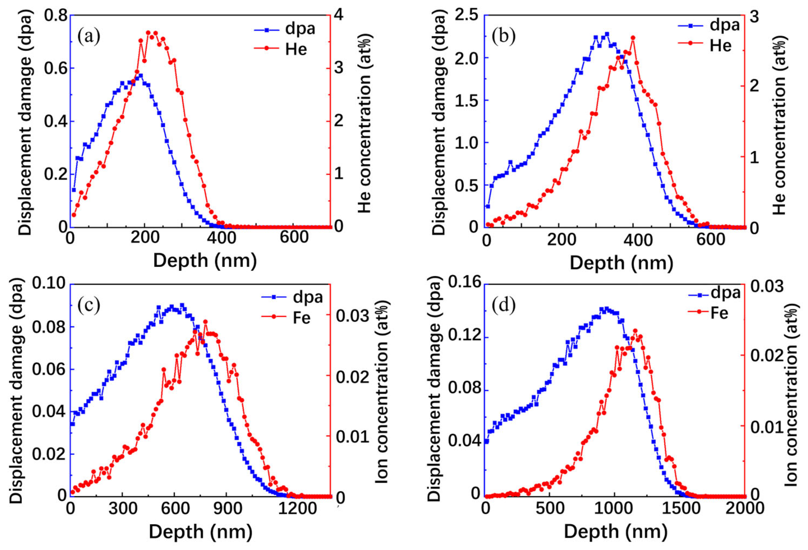
2. Experimental
3. Results and Discussion
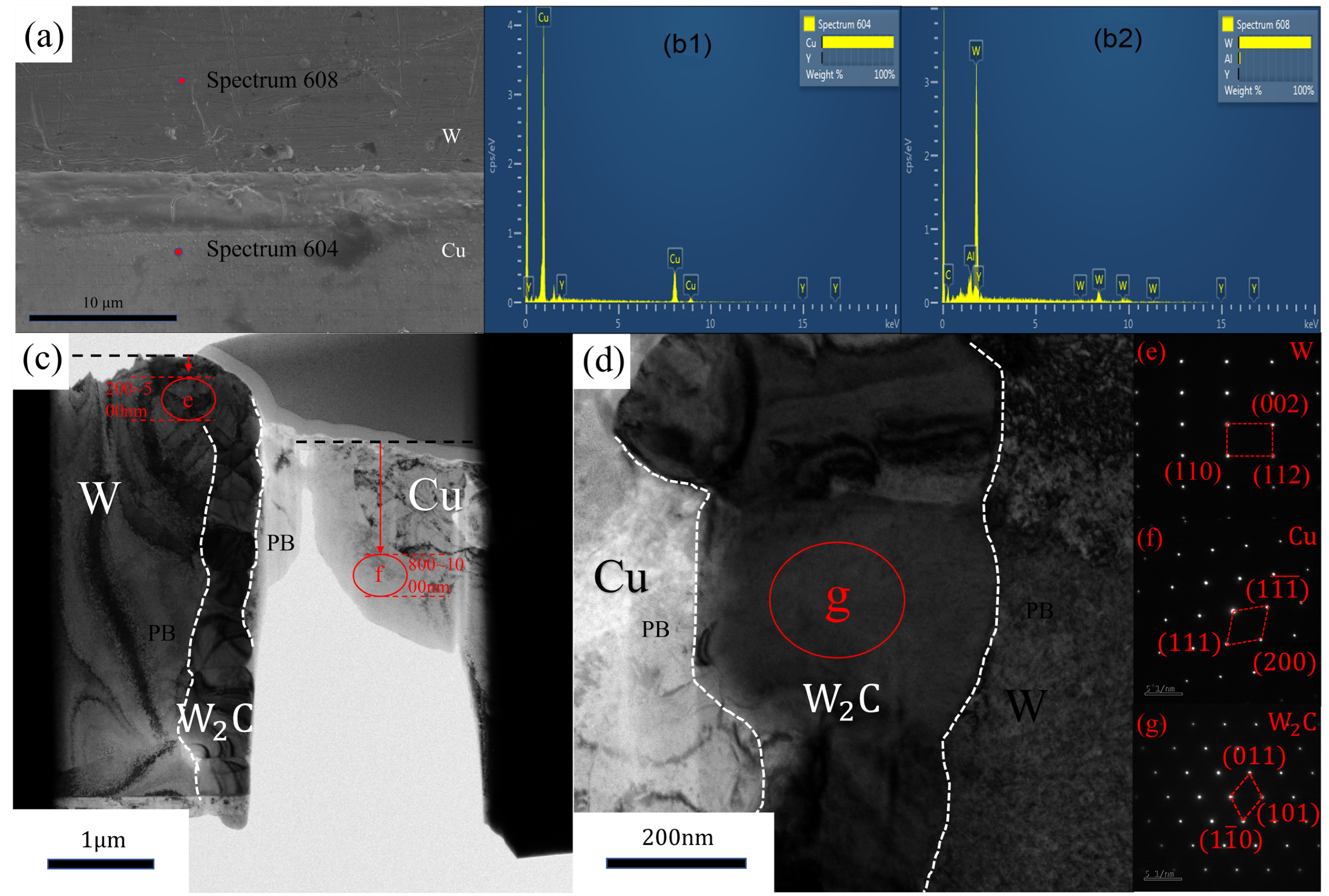
3.1. Microstructure Analysis
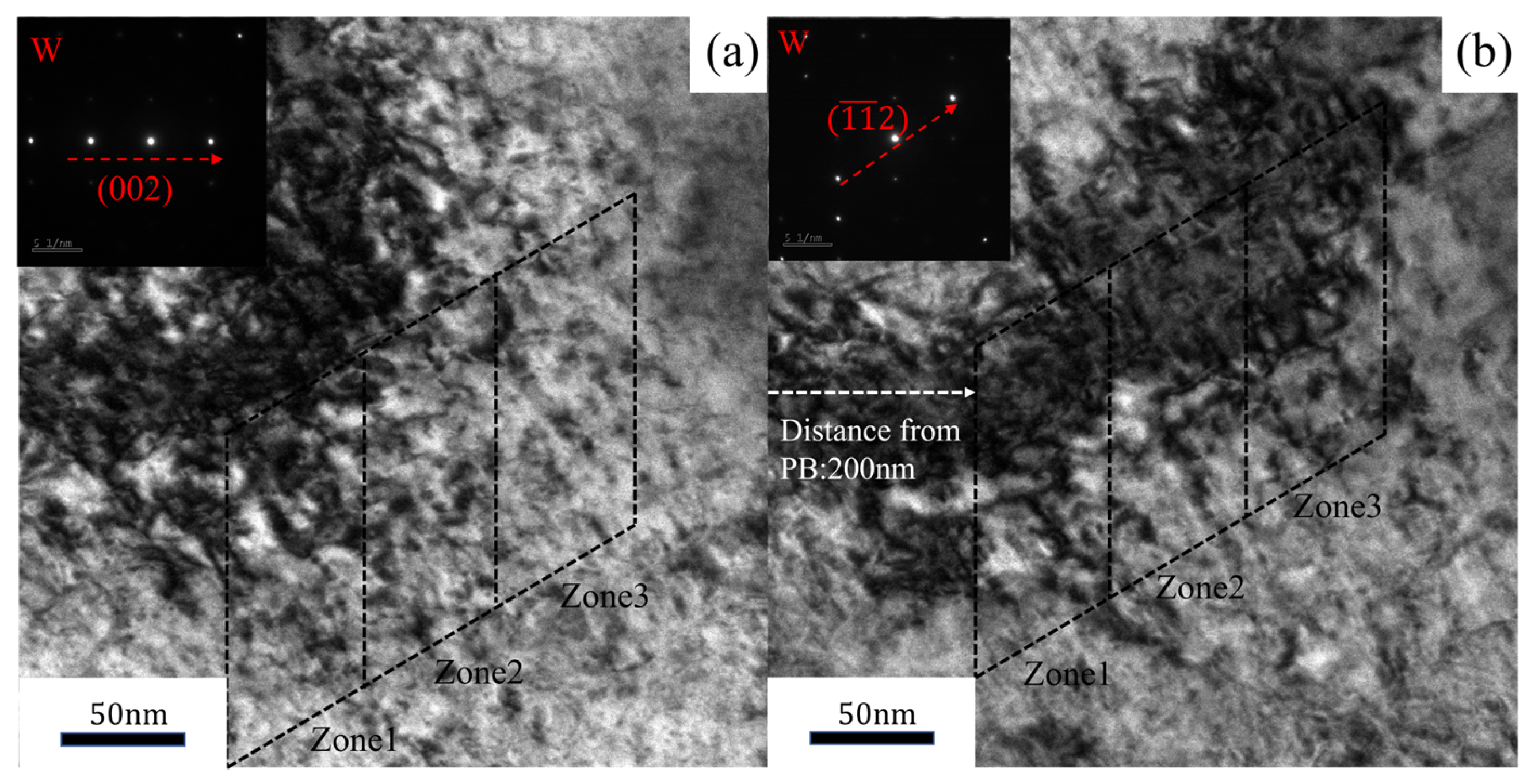
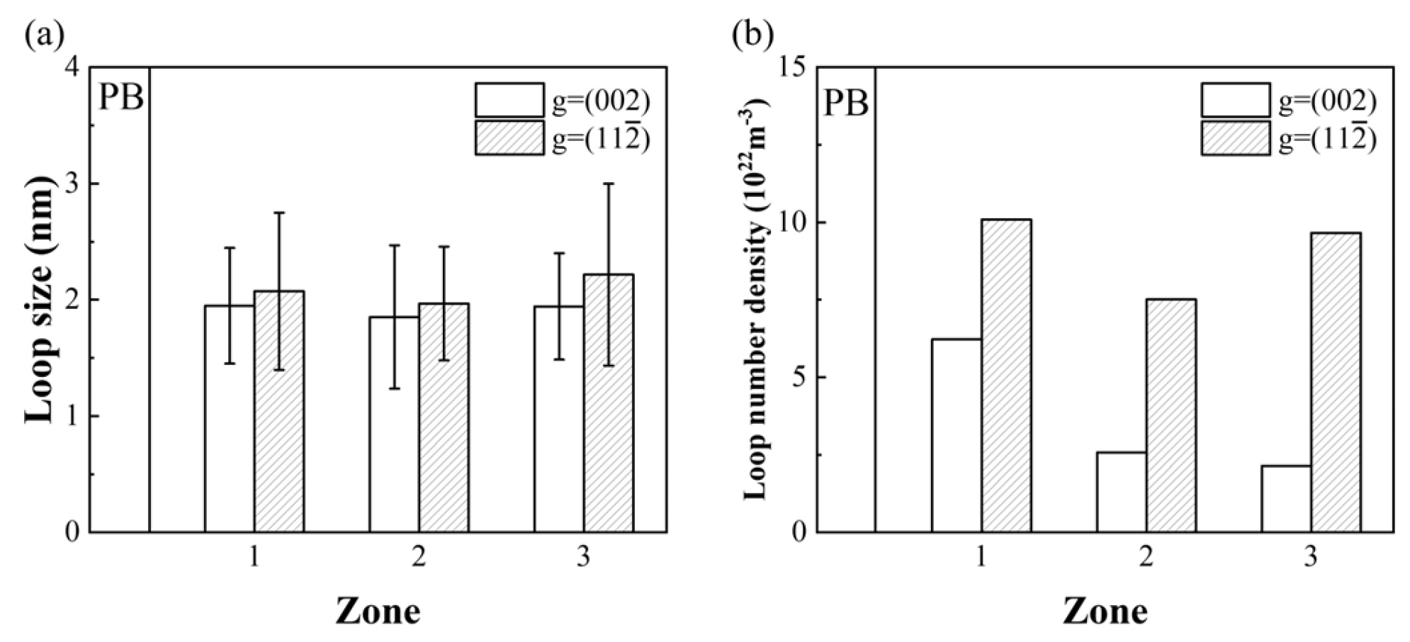
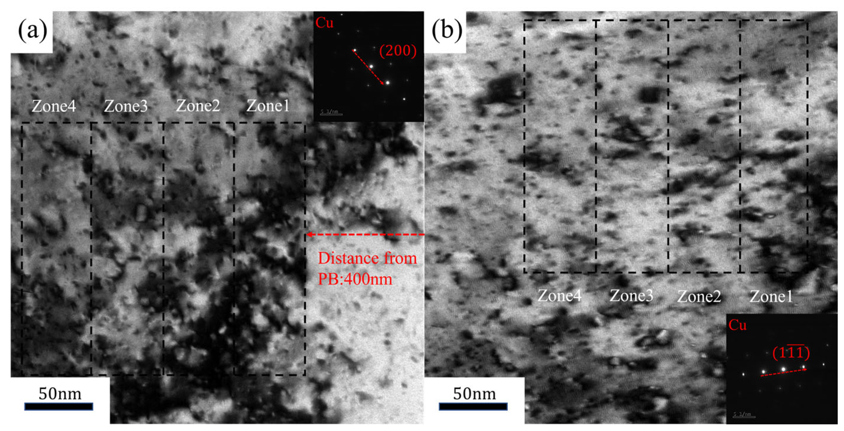
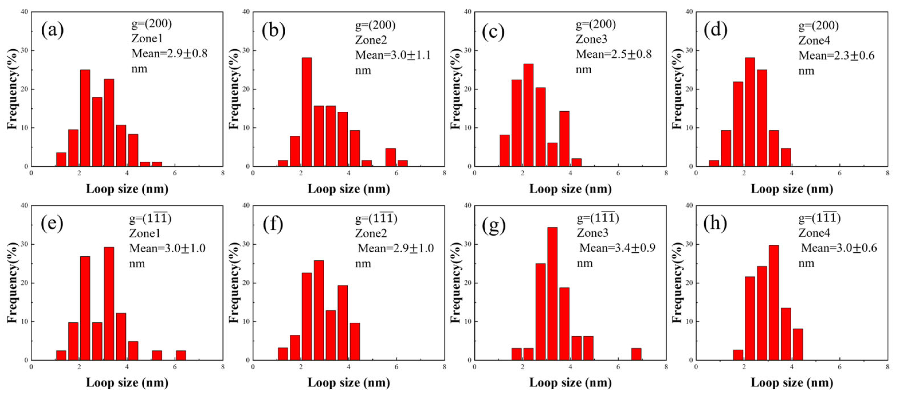
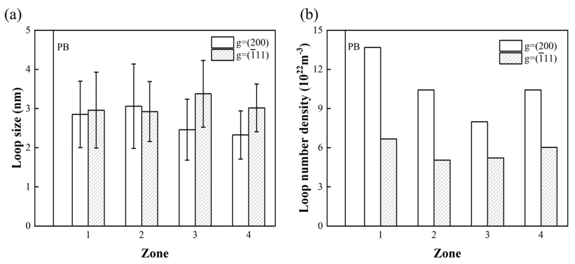
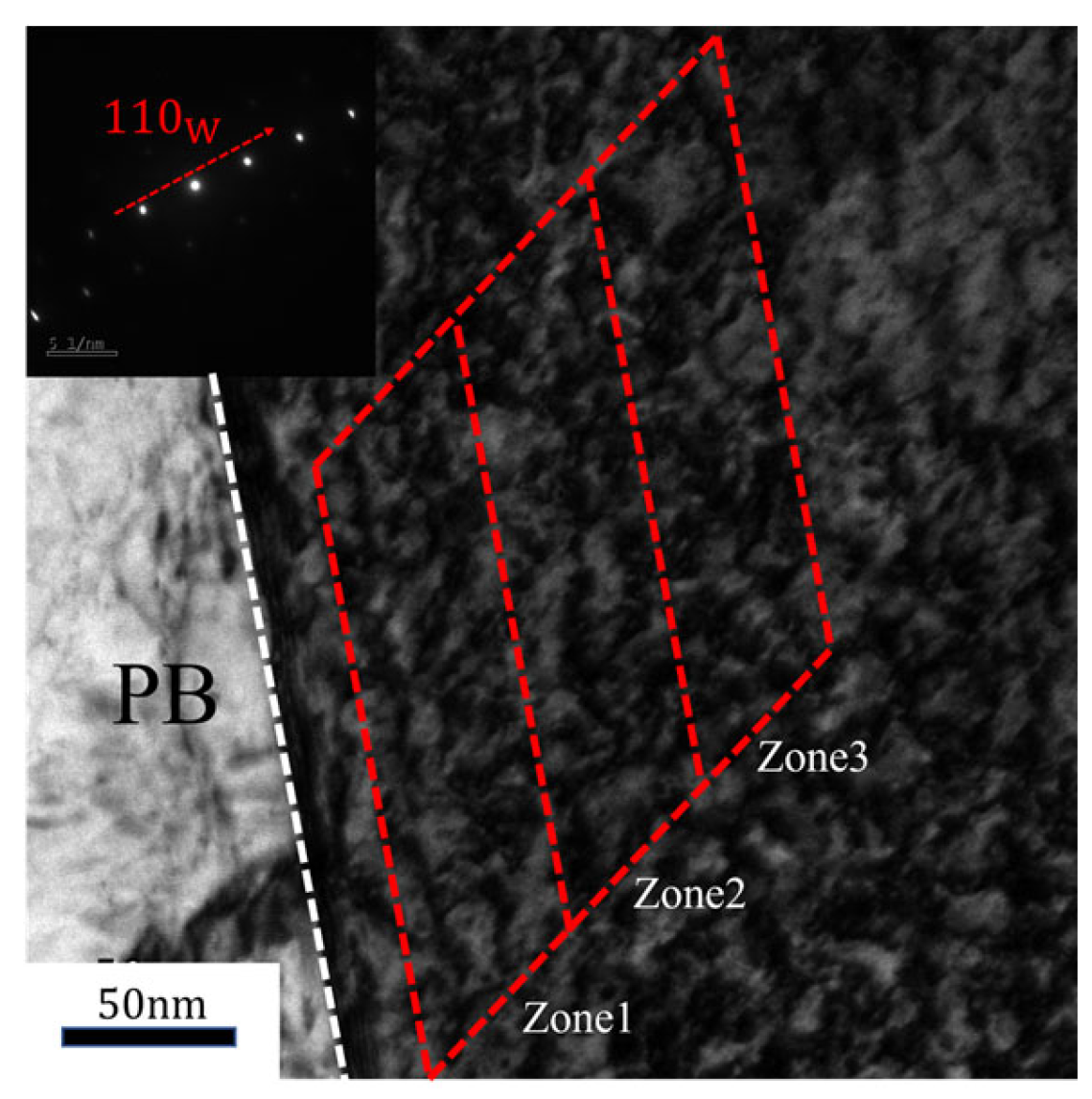
3.2. Radiation-Induced Dislocation Loop After Fe Irradiation
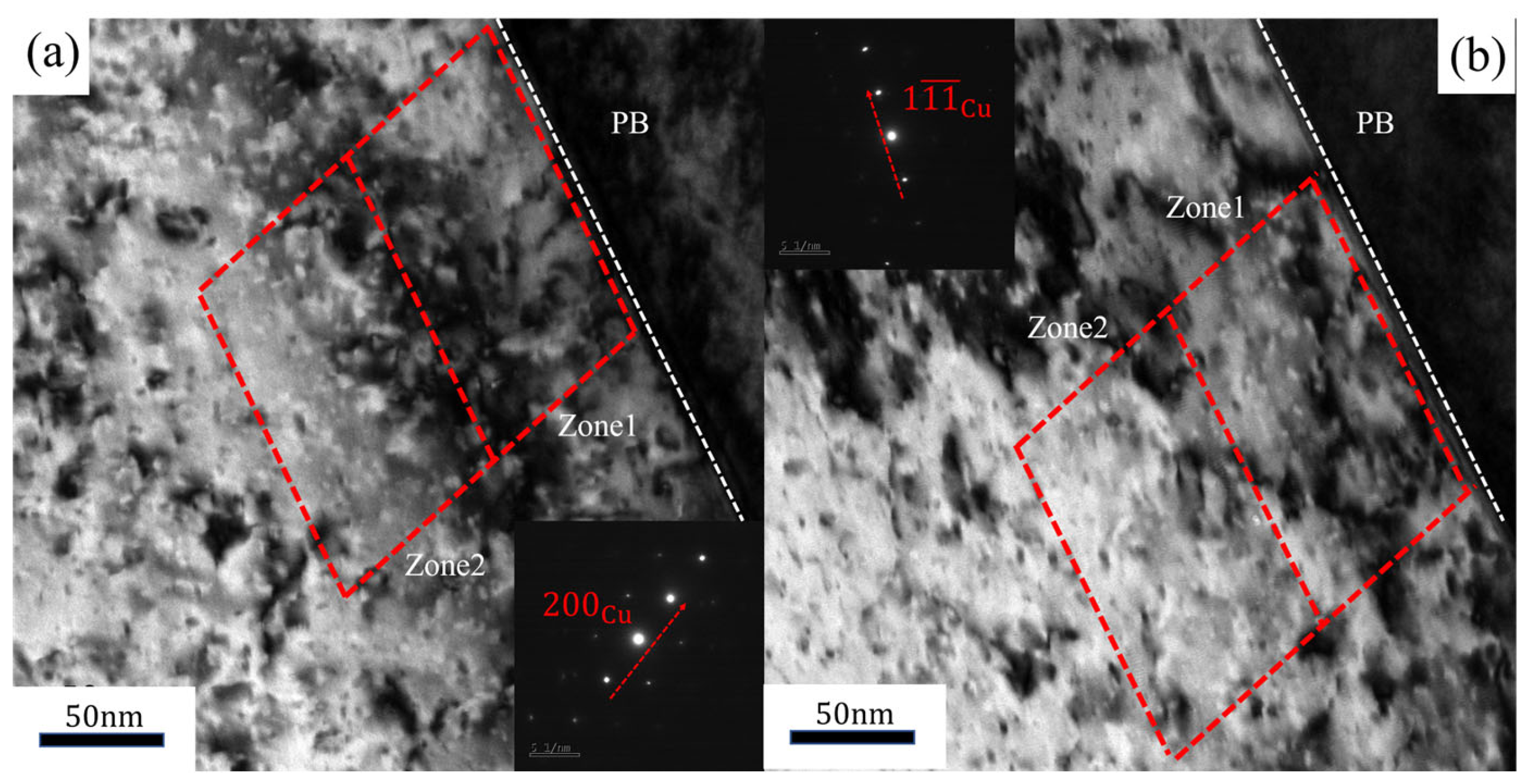
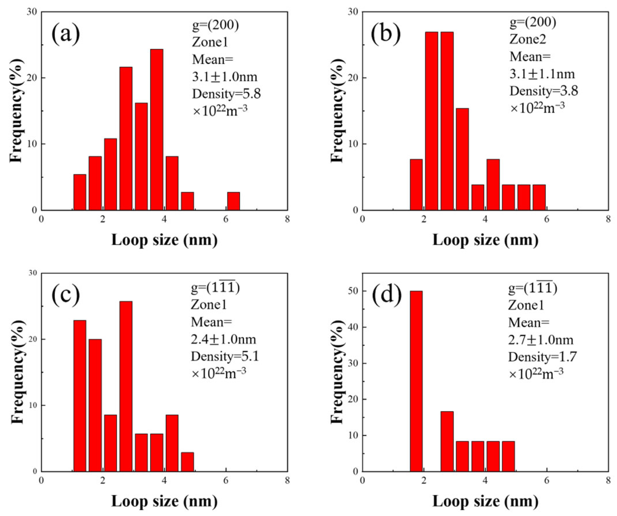
3.3. Radiation-Induced Dislocation Loop After He Irradiation
3.4. The Effect of the W-Cu Phase Boundary
3.5. The Effect of He Atoms
3.6. The Analysis of the Negative Dislocation Loop Density
4. Conclusions
Author Contributions
Funding
Data Availability Statement
Acknowledgments
Conflicts of Interest
References
- Muller, A.V.; Ewert, D.; Galatanu, A.; Milwich, M.; Neu, R.; Pastor, J.Y.; Siefken, U.; Tejado, E.; You, J.H. Melt infiltrated tungsten–copper composites as advanced heat sink materials for plasma facing components of future nuclear fusion devices. Fusion Eng. Des. 2017, 124, 455–459. [Google Scholar] [CrossRef]
- You, J.-H. Copper matrix composites as heat sink materials for water-cooled divertor target. Nucl. Mater. Energy 2015, 5, 7–18. [Google Scholar] [CrossRef]
- Cui, L.J.; Yang, H.L.; Du, Y.F.; Shi, Q.Q.; Kano, S.; Abe, H. TEM characterization of irradiation-induced dislocation loops and voids in ion-irradiated pure chromium. J. Nucl. Mater. 2022, 569, 153920. [Google Scholar] [CrossRef]
- Ando, M.; Hamaguchi, D.; Watanabe, Y.; Nozawa, T. Irradiation hardening and void swelling behaviors of F82H IEA by using dual-ion irradiation. J. Nucl. Sci. Technol. 2023, 60, 1116–1124. [Google Scholar] [CrossRef]
- Wei, G.; Ren, F.; Qin, W.; Hu, W.; Deng, H.; Jiang, C. Evolution of helium bubbles below different tungsten surfaces under neutron irradiation and non-irradiation conditions. Comput. Mater. Sci. 2018, 148, 242–248. [Google Scholar] [CrossRef]
- Patino, M.I.; Nishijima, D.; Baldwin, M.J.; Tynan, G.R. The dependence of tungsten fuzz layer thickness and porosity on tungsten deposition rate and helium ion fluence. Nucl. Fusion 2024, 64, 016011. [Google Scholar] [CrossRef]
- Kuleshova, E.A.; Gurovich, B.A.; Bukina, Z.V.; Frolov, A.S.; Maltsev, D.A.; Krikun, E.V.; Zhurko, D.A.; Zhuchkov, G.M. Mechanisms of radiation embrittlement of VVER-1000 RPV steel at irradiation temperatures of (50–400) °C. J. Nucl. Mater. 2017, 490, 247–259. [Google Scholar] [CrossRef]
- Chen, H.; Xu, Q.; Wang, J.; Li, P.; Yuan, J.; Lyu, B.; Wang, J.; Tokunaga, K.; Yao, G.; Luo, L.; et al. Effect of surface quality on hydrogen/helium irradiation behavior in tungsten. Nucl. Eng. Technol. 2022, 54, 1947–1953. [Google Scholar] [CrossRef]
- Du, J.L.; Chen, H.Q.; Xu, C.; Fan, Y.; Qiu, Y.H.; Wang, H.; Fu, E.G. Stress of misfit dislocation at Fe/MgO interface drives the annihilation of radiation induced defects. Acta Mater. 2021, 210, 116798. [Google Scholar] [CrossRef]
- Wang, M.; Beyerlein, I.J.; Zhang, J.; Han, W.-Z. Defect-interface interactions in irradiated Cu/Ag nanocomposites. Acta Mater. 2018, 160, 211–223. [Google Scholar] [CrossRef]
- Kozlov, A.; Kozlov, K.; Portnykh, I. The evolution of helium-vacancy bubbles in austenitic steels under neutron irradiation. J. Nucl. Mater. 2021, 549, 152915. [Google Scholar] [CrossRef]
- Oda, Y.; Ito, A.M.; Takayama, A.; Nakamura, H. First-Principles Study on Migration of Vacancy in Tungsten. Plasma Fusion Res. 2014, 9, 3401117. [Google Scholar] [CrossRef]
- Ran, Q.; Wang, H.; Zhong, R.; Wu, J.-C.; Zou, Y.; Wang, J. Diffusion behavior of di-interstitials with different configurations in tungsten. Acta Phys. Sin. 2019, 68, 126701.1–126701.8. [Google Scholar] [CrossRef]
- Keys, L.K.; Moteff, J. Neutron irradiation and defect recovery of tungsten. J. Nucl. Mater. 1970, 34, 260–280. [Google Scholar] [CrossRef]
- Bowkett, K.M.; Ralph, B. The Annealing of Radiation Damage in Tungsten Investigated by Field-Ion Microscopy. Proc. R. Soc. London Ser. A Math. Phys. Sci. 1969, 312, 51–63. [Google Scholar]
- Nguyen-Manh, D.; Dudarev, S.L. Trapping of He clusters by inert-gas impurities in tungsten: First-principles predictions and experimental validation. Nucl. Instrum. Methods Phys. Res. Sect. B Beam Interact. Mater. At. 2015, 352, 86–91. [Google Scholar] [CrossRef]
- Yang, L.; Wirth, B.D. Carbon clustering and effect on hydrogen trapping in tungsten: A first-principles study. Comput. Mater. Sci. 2020, 184, 109932. [Google Scholar] [CrossRef]
- Harrison, R.W.; Greaves, G.; Hinks, J.A.; Donnelly, S.E. A study of the effect of helium concentration and displacement damage on the microstructure of helium ion irradiated tungsten. J. Nucl. Mater. 2017, 495, 492–503. [Google Scholar] [CrossRef]
- Ipatova, I.; Harrison, R.W.; Wady, P.T.; Shubeita, S.M.; Terentyev, D.; Donnelly, S.E.; Jimenez-Melero, E. Structural defect accumulation in tungsten and tungsten-5wt% tantalum under incremental proton damage. J. Nucl. Mater. 2018, 501, 329–335. [Google Scholar] [CrossRef]
- Yi, X.; Jenkins, M.L.; Hattar, K.; Edmondson, P.D.; Roberts, S.G. Characterisation of radiation damage in W and W-based alloys from 2MeV self-ion near-bulk implantations. Acta Mater. 2015, 92, 163–177. [Google Scholar] [CrossRef]
- Yi, X.; Jenkins, M.L.; Kirk, M.A.; Zhou, Z.; Roberts, S.G. In-situ TEM studies of 150 keV W + ion irradiated W and W-alloys: Damage production and microstructural evolution. Acta Mater. 2016, 112, 105–120. [Google Scholar] [CrossRef]
- Li, Y.; Wang, L.; Ran, G.; Yuan, Y.; Wu, L.; Liu, X.; Qiu, X.; Sun, Z.; Ding, Y.; Han, Q.; et al. In-situ TEM investigation of 30 keV he + irradiated tungsten: Effects of temperature, fluence, and sample thickness on dislocation loop evolution. Acta Mater. 2021, 206, 116618. [Google Scholar] [CrossRef]
- Xiu, P.; Bei, H.; Zhang, Y.; Wang, L.; Field, K.G. STEM Characterization of Dislocation Loops in Irradiated FCC Alloys. J. Nucl. Mater. 2021, 544, 152658. [Google Scholar] [CrossRef]
- Li, Y.; Ran, G.; Guo, Y.; Sun, Z.; Liu, X.; Li, Y.; Qiu, X.; Xin, Y. The evolution of dislocation loop and its interaction with pre-existing dislocation in He+-irradiated molybdenum: In-situ TEM observation and molecular dynamics simulation. Acta Mater. 2020, 201, 462–476. [Google Scholar] [CrossRef]
- Li, R.; Yi, X.; Han, W.; Liu, P.; Zhan, Q.; Matsukawa, Y.; Watanabe, H.; Wan, F. Micron-scale 1D migration of interstitial-type dislocation loops in aluminum. Mater. Charact. 2023, 203, 113149. [Google Scholar] [CrossRef]
- Du, Y.-F.; Cui, L.-J.; Han, W.-T.; Wan, F.-R. Formation of Vacancy-Type Dislocation Loops in Hydrogen-Ion-Implanted Fe–Cr Alloy. Acta Metall. Sin. Engl. Lett. 2019, 32, 566–572. [Google Scholar] [CrossRef]
- Huang, Y.-N.; Wan, F.-R.; Jiao, Z.-J. The type identification of dislocation loops by TEM and the loop formation in pure Fe implanted with H+. Acta Phys. Sin. 2011, 60, 036802. [Google Scholar] [CrossRef]
- Was, G.S. Fundamentals of Radiation Materials Science: Metals and Alloys; Springer: Berlin, Germany, 2007. [Google Scholar]
- Williams, D.B.; Carter, C.B. Transmission Electron Microscopy: A Textbook for Materials Science; Springer: Berlin, Germany, 1996. [Google Scholar]
- Kinchin, G.H.; Pease, R.S. The Displacement of Atoms in Solids by Radiation. Rep. Prog. Phys. 1955, 18, 1. [Google Scholar] [CrossRef]
- E521; Standard Practice for Neutron Radiation Damage Simulation by Charged-Particle Irradiation. ASTM International: Montgomery County, PA, USA, 1984.
- Patterson, R.J.; Mayer, D.; Weaver, L.; Phaneuf, M. “H-Bar Lift-Out” and “Plan-View Lift-Out”: Robust, Re-thinnable FIB-TEM Preparation for Ex-Situ Cross-Sectional and Plan-View FIB Specimen Preparation. Microsc. Microanal. 2002, 8, 566–567. [Google Scholar] [CrossRef]
- Li, Y.; Gao, Y.; Xiao, B.; Min, T.; Fan, Z.; Ma, S.; Xu, L. Theoretical study on the stability, elasticity, hardness and electronic structures of W–C binary compounds. J. Alloys Compd. 2010, 502, 28–37. [Google Scholar] [CrossRef]
- Liu, X.; Li, Y.; Ran, G.; Ding, Y.; Huang, X. In-situ TEM analysis on early-stage evolution of dislocation loops in 30 keV H2+ irradiated W. Mater. Sci. Eng. A 2022, 852, 143730. [Google Scholar] [CrossRef]
- Ding, Y.-F.; Li, Y.-P.; Liu, X.-Y.; Ran, G.; Huang, X.-Y.; Han, Q.; Chen, Y.; Huang, J.-C.; Zhou, Z.-H. In-situ transmission electron microscopy observation of the evolution of dislocation loops and gas bubbles in tungsten during H2+ and He+ dual-beam irradiation. Tungsten 2021, 3, 434–447. [Google Scholar] [CrossRef]
- Li, R.; Xue, L.; Watanabe, H.; Yi, X.; Han, W.; Liu, P.; Zhan, Q.; Wan, F. Effect of Mn addition on the formation of vacancy-type dislocation loops in α-Fe. Mater. Charact. 2022, 185, 111755. [Google Scholar] [CrossRef]
- Yang, G.; Wu, Y.; Ding, Y.; Li, Y.; Cao, Z.; Li, G.; Cui, D.; He, K.; Qiu, X.; Ran, G. Effect of ion flux on one-dimensional migration of dislocation loops in Fe9Cr1.5W0.4Si F/M steel during in-situ Fe+ irradiation. J. Nucl. Mater. 2023, 579, 154412. [Google Scholar] [CrossRef]
- Becquart, C.S.; Domain, C. Migration Energy of He in W Revisited by Ab Initio Calculations. Phys. Rev. Lett. 2006, 97, 196402. [Google Scholar] [CrossRef]
- Wichert, T.; Deicher, M.; Grübel, G.; Recknagel, E.; Reiner, W. Migration of Helium Atoms in Copper at 25 K. Phys. Rev. Lett. 1985, 55, 726–729. [Google Scholar] [CrossRef]
- Li, X.-C.; Shu, X.; Liu, Y.-N.; Yu, Y.; Gao, F.; Lu, G.-H. Analytical W–He and H–He interatomic potentials for a W–H–He system. J. Nucl. Mater. 2012, 426, 31–37. [Google Scholar] [CrossRef]
- Yi, X.; Han, W.; Liu, P.; Ferroni, F.; Zhan, Q.; Wan, F. Defect Production, Evolution and Thermal Recovery Mechanisms in Radiation Damaged Tungsten. Acta Met. Sin 2020, 57, 257–271. [Google Scholar]


| ρ100(1022m−3) | ρ111(1022m−3) | ρ111/ρ100 | |
|---|---|---|---|
| Zone 1 | 7.2 | 3.8 | 0.53 |
| Zone 2 | 7.4 | 0.1 | 0.01 |
| Zone 3 | 10.7 | / * | / * |
| ρ110(1022m−3) | ρ111(1022m−3) | |
|---|---|---|
| Zone 1 | 42.0 | / * |
| Zone 2 | 32.2 | / * |
| Zone 3 | 16.6 | / * |
| Zone 4 | 26.4 | / * |
| Item | b or g | Density (1021 m−3) | b or g | Density (1021 m−3) |
|---|---|---|---|---|
| Hypothetical dislocation distribution | b = [100] | 3.00 | b = 1/2 [111] | 0.10 |
| b = [010] | 3.00 | b = 1/2 [11] | 0.10 | |
| b = [001] | 1.00 | b = 1/2 [11] | 0.10 | |
| b = 1/2 [11] | 0.10 | |||
| b = <100> | 7.00 | b = 1/2<111> | 0.40 | |
| Measured loop density with different g vector | g = (002) | 1.40 | g = (112) | 7.30 |
| Calculated loop density | b = <100> | 8.33 | b = <111> | −1.38 |
Disclaimer/Publisher’s Note: The statements, opinions and data contained in all publications are solely those of the individual author(s) and contributor(s) and not of MDPI and/or the editor(s). MDPI and/or the editor(s) disclaim responsibility for any injury to people or property resulting from any ideas, methods, instructions or products referred to in the content. |
© 2025 by the authors. Licensee MDPI, Basel, Switzerland. This article is an open access article distributed under the terms and conditions of the Creative Commons Attribution (CC BY) license (https://creativecommons.org/licenses/by/4.0/).
Share and Cite
Sang, H.; Zhang, Y.; Wang, J. The Effect of He on the Evolution of Radiation-Induced Dislocation Loops near W/Cu Interface. Metals 2025, 15, 382. https://doi.org/10.3390/met15040382
Sang H, Zhang Y, Wang J. The Effect of He on the Evolution of Radiation-Induced Dislocation Loops near W/Cu Interface. Metals. 2025; 15(4):382. https://doi.org/10.3390/met15040382
Chicago/Turabian StyleSang, Huaqing, Yifan Zhang, and Jing Wang. 2025. "The Effect of He on the Evolution of Radiation-Induced Dislocation Loops near W/Cu Interface" Metals 15, no. 4: 382. https://doi.org/10.3390/met15040382
APA StyleSang, H., Zhang, Y., & Wang, J. (2025). The Effect of He on the Evolution of Radiation-Induced Dislocation Loops near W/Cu Interface. Metals, 15(4), 382. https://doi.org/10.3390/met15040382