Abstract
Electromigration is one of the most important research issues affecting the reliability of solder joints. Current-induced Joule heating affects the electromigration behavior of solder joints. Solder joints with different cross-sectional areas were designed to obtain different Joule heating properties. The effects of the interfacial intermetallic compound (IMC) and mechanical properties of Sn58Bi/Cu solder joints were studied for different Joule heating properties. The results showed that as the cross-sectional area of the Sn58Bi/Cu solder joints increased, the Joule heating of the joint increased. The anode IMC thickness of the joint thickened and transformed into a planar shape. The Bi migrated to the anode region to form a Bi-rich layer and gradually increased in thickness. The cathode IMC thickness first increased, then decreased, and gradually dissolved. The Sn-rich layer formed near the solder side and gradually increased in thickness, with microcracks occurring when the cross-sectional area of the joint increased to 0.75 mm2. The joint shear fracture path moved from the soldering zone near the cathode IMC layer to the interfacial IMC layer. The fracture mechanism of the joint changed from a mixed brittle/tough fracture, dominated by deconstruction and secondary cracking, to a brittle fracture dominated by deconstruction. The joint shear strength was reduced by 60.9% compared to that in the absence of electromigration.
Keywords:
Sn58Bi; solder joint; Joule heat; electromigration; interfacial IMC; mechanical properties 1. Introduction
For electronic packaging solder joints, the performance of the solder material directly determines the performance of the solder joint [1,2]. The conventional SnPb solder is widely used, attributed to its low melting point and cost, as well as excellent wettability and mechanical properties [3]. With the progress of lead-free solders, SnPb has been gradually abandoned due to the great harm to human beings and the environment, and there have been efforts to obtain a lead-free solder that can mimic the properties of SnPb solders [4,5,6,7,8]. The SnBi solder has received great attention due to its low cost, low melting point and high strength, and it is widely used in low-temperature packaging for electronic products [9].
As the current development of electronic products favors miniaturization and integration, the scale of micro-solder joints is becoming smaller, resulting in an increase in the current density carried by the solder joints [10,11,12]. At high current densities, solder joints generate not only electromigration [13,14] but also a large amount of Joule heat [15,16], which seriously affects the reliability of solder joints and has become one of the most important areas in current research [17,18,19].
Thus far, domestic and international research on electromigration has focused on the effect of the external environment’s temperature on the reliability of solder joints. Nguyen et al. [20] studied the correlation between electromigration and rapid thermal cycling; their results showed that rapid thermal cycling significantly shortened the electromigration lifetime of solder joints, and this was mainly dependent on the thermal cycling temperature range and minimum temperature, etc. Cui et al. [21] performed a simulation study of the electromigration electrothermal coupling of metal interconnects and found that the current density was the main factor affecting the electromigration lifetime of interconnects in a certain temperature range, with the temperature variation having a smaller effect. Wang et al. [22] found that Cu/Sn-58Bi/Cu solder joints exhibited different electromigration current density thresholds at different ambient temperatures. This reflects the temperature dependence of the minimum current density in this soldering material, which triggers the directional migration of atoms and is consistent with the results of Basaran et al. [23], who reported a high ambient temperature, fast electromigration rate, and fast accumulation of the Bi-rich layer in the anode region. Gu et al. [24] calculated the intrinsic diffusion coefficient D0 as 9.91 × 10⁻⁵ m2/s and the activation energy as 89.2 kJ/mol (0.92 eV) for a Cu-Sn IMC based on the effect of environment temperature electromigration on the growth of the Cu-Sn IMC layer in Cu/SnBi/Cu solder joints. Xu et al. [25] studied the electromigration of eutectic SnBi/Cu solder joints at different temperatures; their results showed that Sn exhibited different diffusion properties at high and low temperatures.
As research progressed, the Joule heat generated by the solder joint itself during electromigration was shown to have a more significant effect on the joint reliability than the environmental temperature. Guo et al. [26] adopted a special linear symmetric structure and observed an unusual Sn atomic thermal migration (TM) phenomenon in Sn58Bi solder joints, in which Joule heat led to an increase in joint temperature that favored the occurrence of TM. Ouyang et al. [27] found that eutectic SnPb solder joints underwent recrystallization under the effect of Joule heating to refine the joint organization. Chiu et al. [28] used thermal infrared microscopy and modeling to investigate the Joule heating effect in solder joints and found that hot spots were created during electromigration in solder joints under the effect of Joule heating and played an important role in the formation of initial voids. Nah et al. [29] studied the electromigration of 97Pb-3Sn and 37Pb-63Sn composite solder joints at room temperature, and they found that higher Joule heat allowed Pb to migrate more easily.
Thus far, domestic and international studies on the correlation between electromigration and temperature have been implemented mainly using a change in the environmental temperature to change the solder joint temperature [30,31], whereas studies on the effect of the solder joint temperature and its resulting Joule heat on electromigration in the solder joint have rarely been reported in the literature.
In this paper, Sn58Bi solder material was used as the research object to achieve different Joule heating properties through the design of different solder joints. The organization and mechanical properties of electromigration joints with different Joule heating properties were investigated to provide an experimental basis for the design of highly reliable solder joints.
2. Materials and Methods
2.1. Materials
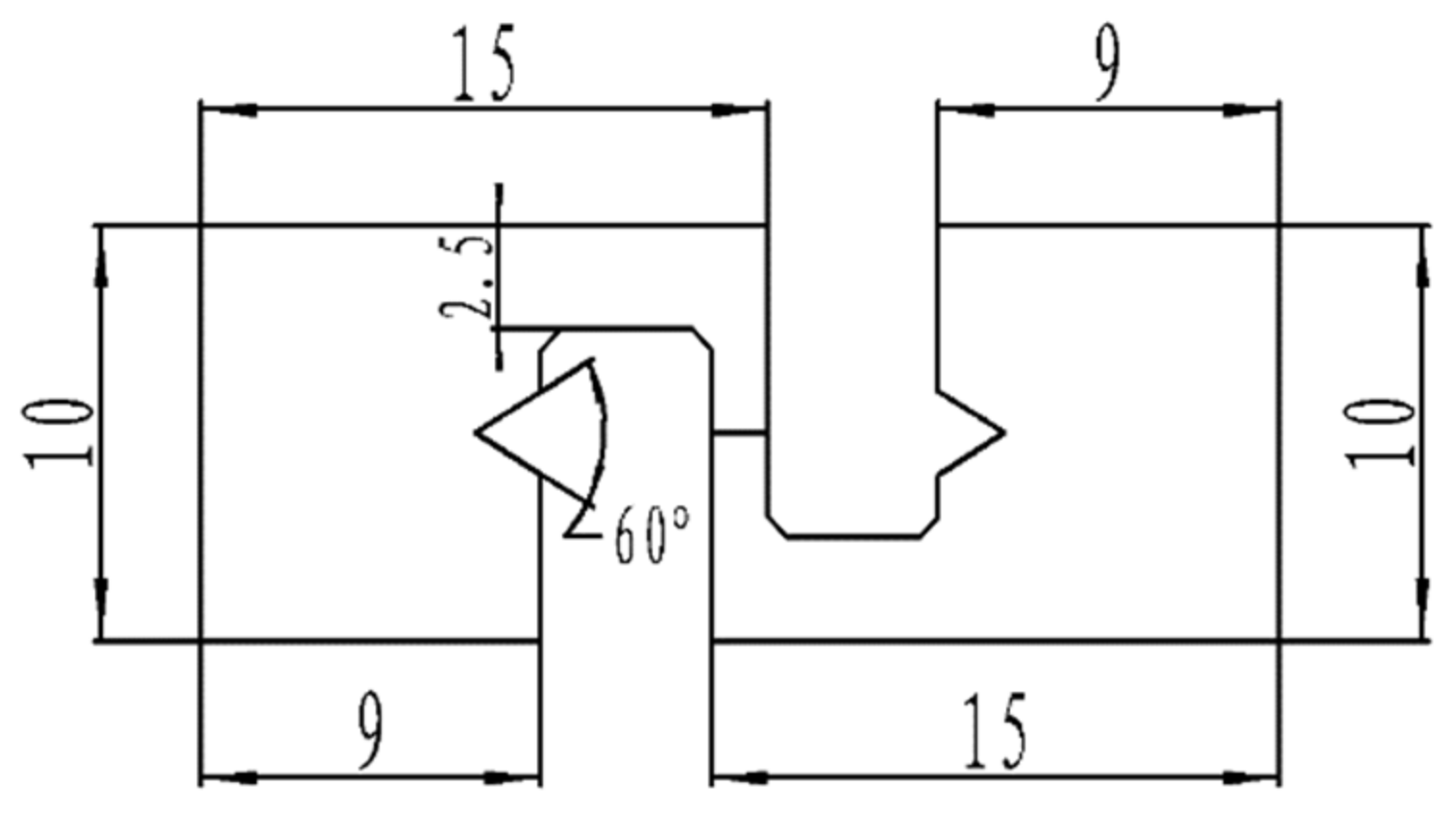
Materials including Sn58Bi, a copper sheet purchased from Changsha Tijo Metal Material Co., Ltd., and the Sn58Bi filler metal were used in this study, and the filler metal was rolled into a solder foil with a thickness of 0.1 mm [32,33]. The base material for the soldering test was a 99.99% pure purple copper sheet. The solder joint size shape, with a thickness of 0.5 mm, is shown in Figure 1, and the soldering flux selected was CX600 washed soldering flux.
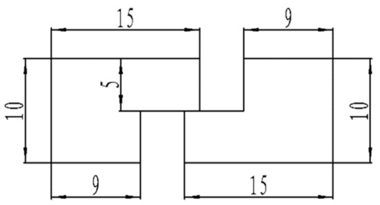
Figure 1.
Schematic diagram of solder joint specimen.
2.2. Experimental Procedures
By varying the cross-sectional area of the solder joint and the applied current magnitude, the current density was kept constant to achieve the purpose of changing the Joule heat environment of the joint. For this purpose, joints with four different cross-sectional areas, 0.25 mm2, 0.5 mm2, 0.75 mm2, and 1.0 mm2, were set up in this test to change the Joule heat magnitude of the solder joints. Before soldering, the solder joint and the filler metal were polished and cleaned; then, 1–2 drops of soldering flux were applied to the solder joint, the filler metal was placed between the copper plate joints and pressed, and the whole joint was placed on the heating platform for the soldering test. The heating platform was set at 210 °C (the solder joint temperature was approximately 190 °C) and soldering was performed for 180 s. After soldering, the solder joint was machined into the shape and size shown in Figure 2, and the solder joint was fixed in a homemade electromigration fixture, as shown in Figure 3.

Figure 2.
Electromigration specimen.
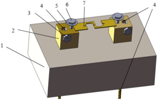
Figure 3.
Schematic diagram of electromigration fixture (1. Insulated carrier table; 2. Copper conductor table; 3. Fixed wire bolts; 4. Connecting wire; 5. Gasket liner; 6. Fixed specimen bolts; 7. Test specimen).
The power supply device was an LW-50100KD direct-current-regulated power supply (DC). The applied current density of the solder joint was 8 × 10³ A/cm2 and the time was 100 h. In order to eliminate the temperature gradient that could be formed in the specimen during electromigration and to avoid the occurrence of heat migration caused by the temperature gradient, the whole test procedure was carried out in a dimethyl silicone oil environment [34].
2.3. Organization and Property Test
After the completion of the electromigration test, the specimen was inlaid using the XQ-2B inlay machine. After grinding and polishing, the specimens were corroded for 8 s with a mixed solution of hydrochloric acid and alcohol with a volume fraction of 5%. The JSM-IT100 tungsten filament scanning electron microscope (SEM) was used to observe the IMC of the solder joints and the tissue morphology of the solder area, and the composition was analyzed with the help of an INCA CH5 energy-dispersive spectrometer (EDS), if necessary. A solution of 20% hydrogen peroxide and 80% glacial acetic acid [35] by volume fraction was used to etch the solder joints and expose the interfacial reaction products, which were analyzed by D8 Advance X-ray diffraction (XRD). The shear strength of the solder joints was tested with a UTM2503 micro-tensile testing machine (tensile rate: 1 mm/min).
3. Results
3.1. Microstructure of Solder Joint before Electromigration
Figure 4 shows the microstructure morphology, EDS composition analysis, and XRD diffraction analysis of the Sn58Bi/Cu solder joint. Table 1 presents the EDS analysis of the labeled regions. As shown in Figure 4, the Sn58Bi/Cu solder joint has three regions: base material, interface, and solder. The base material in the dark gray area on the left side of Figure 4a consists of the Cu substrate, and the light gray area on the right side is the interfacial region, consisting of the scallop-shaped IMC, which is mainly composed of Cu6Sn5, as shown by EDS and XRD analysis, and Bi is not involved in the interfacial IMC reaction. The reason for the formation of Cu6Sn5 IMC is mainly the metallurgical reaction between the Cu substrate and the Sn in the filler metal during the soldering process [36,37]. The solder zone is a typical layered eutectic consisting of the β-Sn phase and the Bi-rich phase. The EDS analysis shows the white phase in the solder zone, which is the Bi-rich phase, and the gray phrase, which is the β-Sn phase.
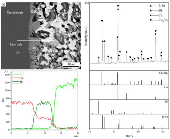
Figure 4.
Micromorphology, EDS analysis, and XRD diffraction pattern of Sn58Bi/Cu soldering joint: (a) micromorphology, (b) EDS component analysis, (c) XRD diffraction pattern, with standard peak pattern of Cu6Sn5, Cu, Bi, and β-Sn.

Table 1.
EDS analysis of different regions of solder joint (At.%).
3.2. Sn58Bi/Cu Solder Joint Temperatures for Different Joule Heating Properties
Even if the current density of the joint is kept constant, the Joule heat generated in solder joints with different cross-sectional areas and different currents is different [38]. The Joule heat generated by the solder joint can be calculated by Equation (1):
In Equation (1), I is the magnitude of the applied current, R is the solder joint resistance, t is the time, is the resistivity, l is the resistive length (i.e., the length of the solder zone), s is the resistive cross-sectional area perpendicular to the current (the joint cross-sectional area), j is the current density, and V is the volume of the solder.
From Equation (1), it can be seen that by keeping the current density constant, the Joule heat increases as the volume of the solder joint increases.
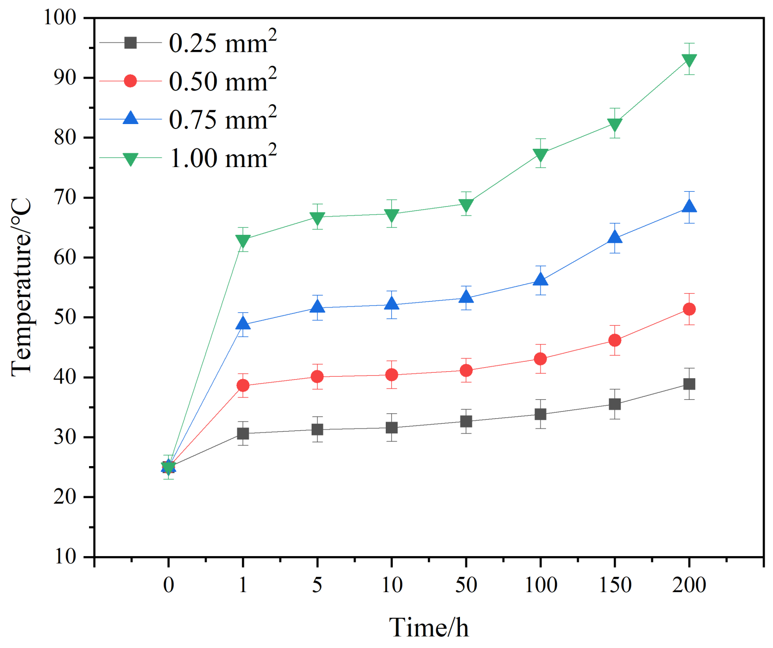
Figure 5 shows the temperature evolution curve of solder joints with different cross-sectional areas and currents. From Figure 5, it can be seen that the temperature change in the solder joint can be divided into three stages: a steep increase, a steady increase, and a slow increase. When the current is first loaded, a large amount of Joule heat accumulates at the joint, causing the temperature of the joint to rise sharply; when the rate of Joule heat accumulation tends towards equilibration with the rate of heat dissipation from the joint, the temperature change tends to be smooth. The temperature also rises gradually as the electromigration time continues to increase, which is mainly due to the gradual migration of elements from the cathode region to the anode region under the action of the current, and the gradual formation of microvoids and cracks in the cathode region, which leads to an increase in the resistance of the joints and a gradual increase in the Joule heat generated by the corresponding joints [39].
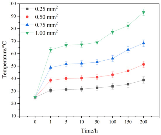
Figure 5.
Temperature evolution curves of solder joints with different joint cross-sectional areas and applied currents.
Solder joints with different cross-sectional areas show a slow increase in temperature after electric loading after a period of time. Different cross-sectional areas require different times for this inclination change: for the area of 1.00 mm2, it occurs at 50 h; for 0.75 mm2, around 100 h; and for the areas of 0.5 and 0.25 mm2, it is above 150 h. If the observation occurs at 50 h, the phenomenon is not obvious enough. If the observation occurs at 150 h or longer, for 1 mm2, it is difficult to achieve a complete joint. Thus, the organization and properties of the test were accordingly selected for the electromigration duration of 100 h.
3.3. Electromigration Organization of Sn58Bi/Cu Solder Joints with Different Joule Heating Properties
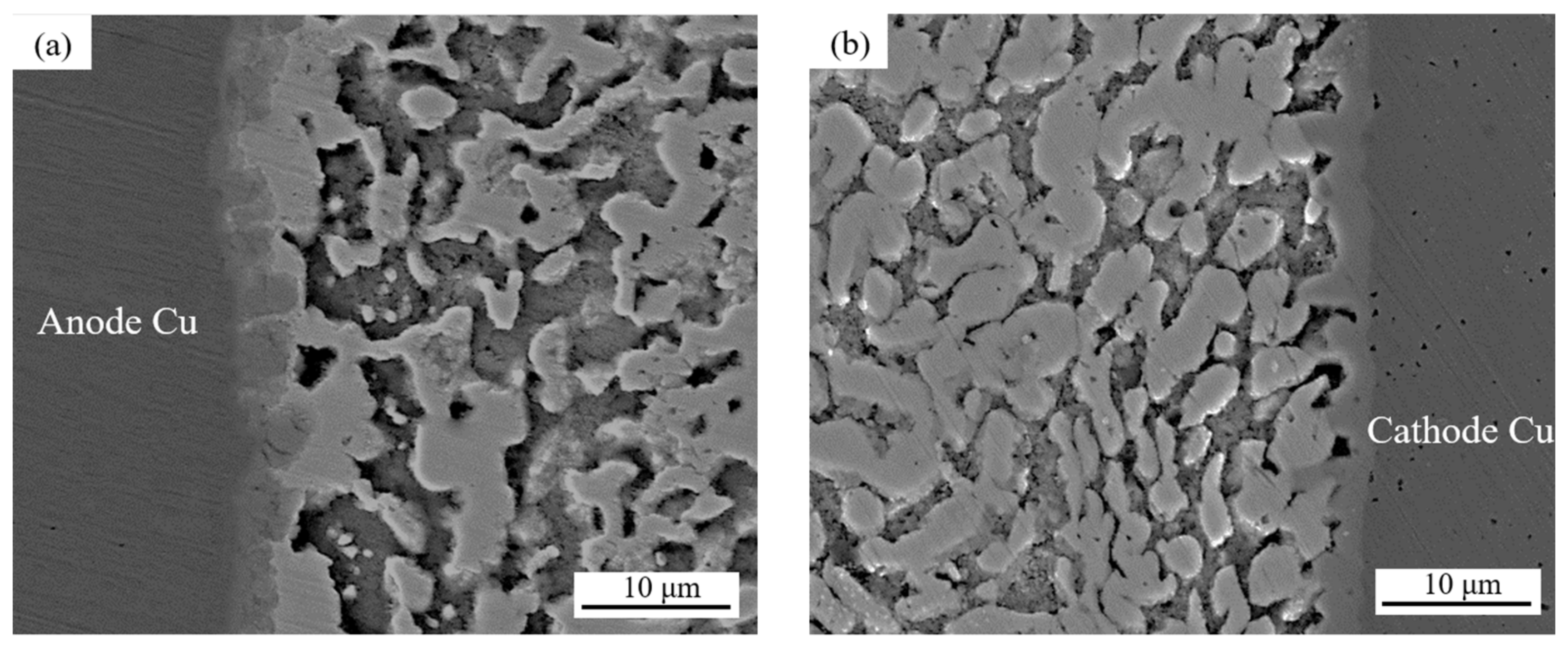
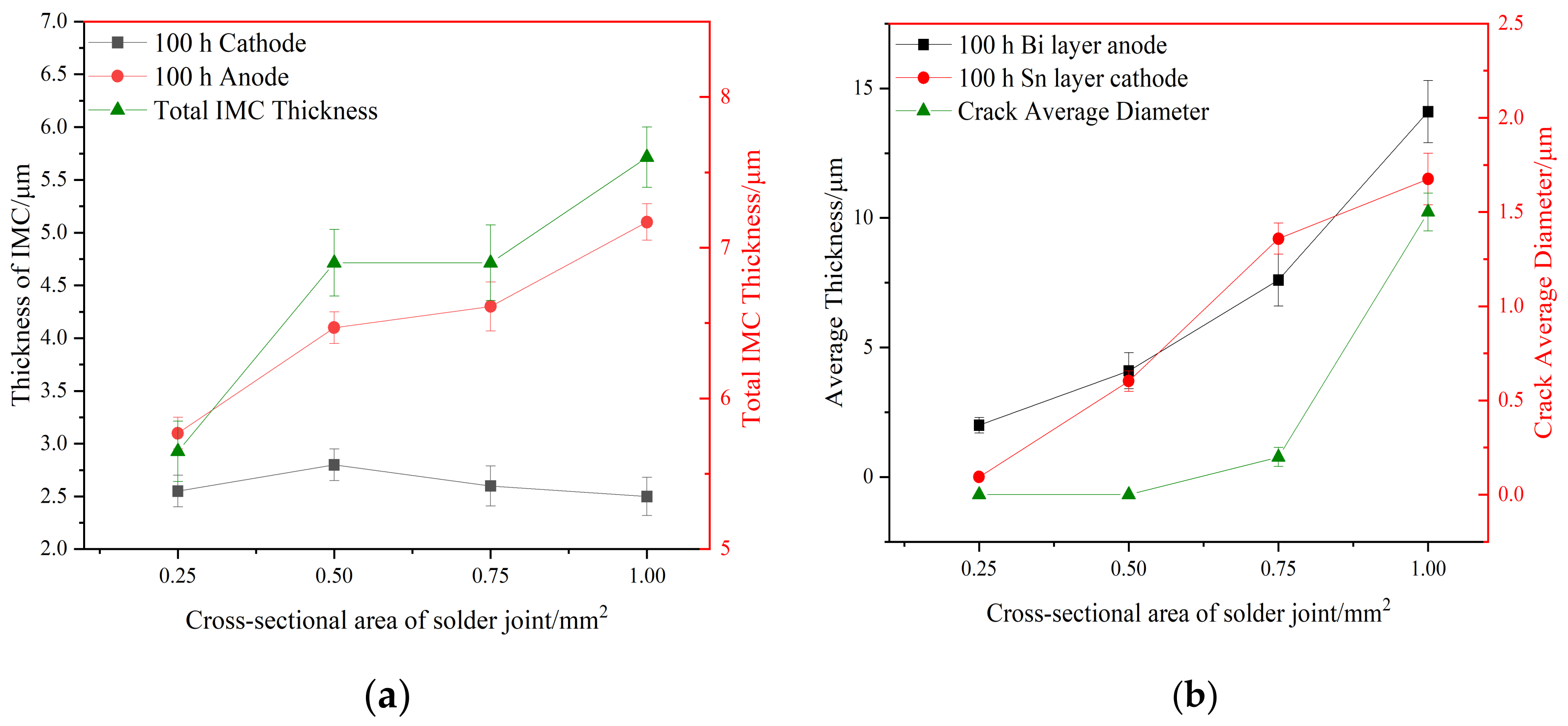
Figure 6 shows the microstructure morphologies of solder joints with different joint cross-sectional areas after 100 h of electromigration at a current density of 8 × 10³ A/cm2, and Figure 7 shows the effect on the IMC thickness and the thickness of the Bi-rich layer of the solder joints. Table 2 presents the EDS analysis of the labeled regions.
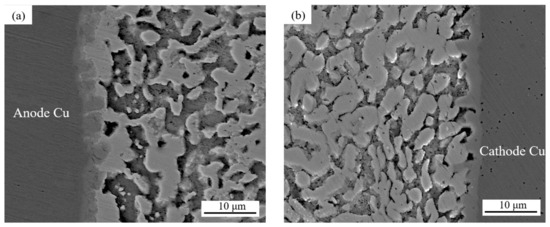

Figure 6.
Evolution of the microstructures of solder joints with different cross-sectional areas and current sizes: (a,b) 0.25 mm2; (c,d) 0.5 mm2; (e,f) 0.75 mm2; (g) zoomed-in images of area A; (h) zoomed-in images of area B; (i,j) 1.0 mm2.
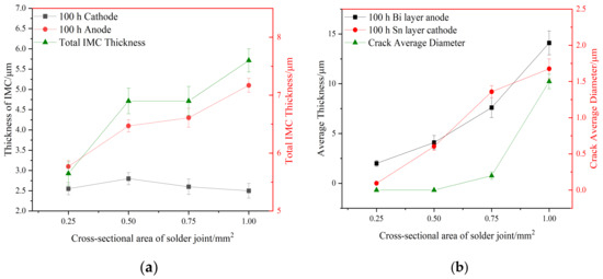
Figure 7.
Influence of different cross-sectional area and current on IMC thickness, Bi rich layer, Sn rich layer thickness, and crack diameter in solder joints. (a) IMC thickness (b) Bi rich layer, Sn rich layer thickness, and crack diameter.
Table 2.
EDS analysis of microcomponents of solder joints with different Joule thermal properties (At.%).
Anode area: As can be seen in Figure 6 and Figure 7, with a joint cross-sectional area of 0.25 mm2, as shown in Figure 6a, the IMC of the solder joint is mainly a scalloped Cu6Sn5 IMC layer in the anode region with an average thickness of 3.1 (±0.15) μm, a vaguely irregularly shaped Bi-rich phase accumulates in the near-soldering seam side of IMC, and an obvious Bi-rich layer has not yet been formed. When the cross-sectional area of the joint is 0.5 mm2, as shown in Figure 6c, the Cu6Sn5 IMC is transformed into a flat plate with an average thickness of 4.1 (±0.15) μm in the anode region, and the irregularly raised Bi-rich layer is transformed into a regular flat plate with an average thickness of 4.1 (±0.7) μm. When the cross-sectional area of the joint is 0.75 mm2, as shown in Figure 6e, the overall Cu6Sn5 IMC in the anode area is in the shape of a flat plate, and the individual scallop-like morphology reappears at the edge, which indicates that the IMC is growing gradually, with an average thickness of 4.3 (±0.23) μm. The morphology of area A in Figure 6e is shown at high magnification in Figure 6g, and the analysis of the composition of area C in Figure 6g indicates that the IMC is Cu6Sn5, with Cu3Sn not appearing, and large Bi-rich phases are migrating to the Bi-rich layer at the outer side of the Bi-rich layer. When the cross-sectional area of the joint is 1.0 mm2, as shown in Figure 6i, there is no obvious change in the morphology of the interface IMC and the Bi-rich layer in the anode area at this time, and the average thickness of the Bi-rich layer increases significantly to 14.1 (±1.2) μm.
Cathode area: At a joint cross-sectional area of 0.25 mm2, as shown in Figure 6b, the IMC morphology in the cathode region consists of short rods and is scalloped, which is not significantly different from the initial morphology. When the cross-sectional area of the joint is 0.5 mm2, as shown in Figure 6d, the IMC grows in the cathode region, resulting in larger short rods and flat plates with an average thickness of 2.8 (±0.14) μm, and a layer of the corresponding Sn-rich zone appears in the IMC near the solder zone. When the cross-sectional area of the joint is 0.75 mm2, as shown in Figure 6f, the IMC in the cathode region is in the form of flat plates and short rods, and the average thickness is reduced to 2.6 (±0.19) μm; part of the IMC is gradually dissolved under the action of the current and diffuses into the solder zone, the thickness of the Sn-rich region is approximately 9.2 (±0.6) μm, and long and thin microcracks appear in the connection between the Sn-rich region and the IMC. The morphology of area B in Figure 6f is shown at high magnification in Figure 6h, and the compositional analysis of area D in Figure 6h reveals that it is mainly composed of Sn. The formation of the Sn-rich region occurs due to the Bi enrichment in the cathode region, which migrates to the anode region under the action of the current, thus generating the Sn-rich region in the cathode region. When the joint cross-sectional area is 1.0 mm2, as shown in Figure 6j, multiple microcracks appear in the IMC of the cathode region, the thickness is reduced to 2.5 (±0.18) μm, and the microcracks in the cathode region are expanded with an average width of 1.5 (±0.1) μm. This is due to the accelerated migration of atoms triggered by electromigration under large Joule heat; atoms’ migration leads to increased microcracking [40,41]. Microcracks lead to a sharp increase in the resistance of the solder joint and, thus, a faster change in the temperature of the joint, which further accelerates the failure of the soldered joint.
From the analysis of Figure 6 and Figure 7, it can be seen that in the electromigration process of Sn58Bi/Cu solder joints, the atoms will continue to migrate from the cathode area to the anode area, in which Bi will first migrate and form an aggregation in the anode area near the solder side of the IMC and gradually form a Bi layer; then, a dense Bi layer will impede the growth of the IMC, the growth of IMC in the anode area will be slowed down, and the cathode area will be gradually thinned out. The total IMC thickness of the cathode and anode does not change when the joint area is increased from 0.5 mm2 to 0.75 mm2.
As the cross-sectional area of the solder joint increases, the thickness of the IMC in the anode region of the joint and the thickness of the Bi-rich layer also increases, which is attributable to the larger Joule heat, which increases the temperature of the solder joint and intensifies the thermal motion of the atoms, according to the diffusion coefficient equation:
In Equation (2), D is the diffusion coefficient, T is the temperature, R is a constant, and Q is the activation energy.
From Equation (2), it can be seen that when the temperature increases, the diffusion coefficient D is also increased, the electromigration rate is relatively accelerated, the Bi aggregation in the anode region is also accelerated, the thickness of the Bi-rich layer is gradually increased, and the thickness of the IMC in the anode region is also gradually increased.
Due to the fast migration of Bi, although the rapid migration of Bi to the anode region forms a Bi-rich layer, the cathode region will correspondingly appear as a Sn-rich region. A large amount of Bi migration increases defects such as crystal vacancies in the cathode region, which encourages atoms to undergo diffusion [42,43]; at this time, the atoms in the IMC in the cathode region migrate faster and the thickness decreases, and when there are fewer microdefects in the cathode region (Figure 6d), the IMC diffuses slower, so the thickness of the IMC increases.
3.4. Mechanical Properties of Sn58Bi/Cu Solder Joints with Different Joint Cross-Sectional Areas
Figure 8 shows the evolution of the average width of the microcracks and shear strength of Sn58Bi/Cu solder joints with different cross-sectional areas after electromigration for 100 h. As can be seen from Figure 8, with the increase in the cross-sectional area of the solder joint, the shear strength of the joint first undergoes a slow decrease, and when the cross-sectional area of the joint is 0.75 mm2, the joint microcracks appear to make the strength of the joint decrease rapidly. When the electromigration time was 100 h and the joint cross-sectional area was increased from 0.5 mm2 to 0.75 mm2, the shear strength of Sn58Bi/Cu solder joints decreased to 19.7 (±2.1) MPa, a decrease of 33.9%. When the cross-sectional area of the joint was increased to 1.0 mm2, the joint shear strength decreased to 13.4 (±2.0) MPa, representing a decrease of 31.9%, and a decrease of 60.9% compared to the absence of electromigration.
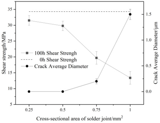
Figure 8.
Electromigration shear strength and average crack size of Sn58Bi/Cu solder joints at different cross-sectional areas and current densities.
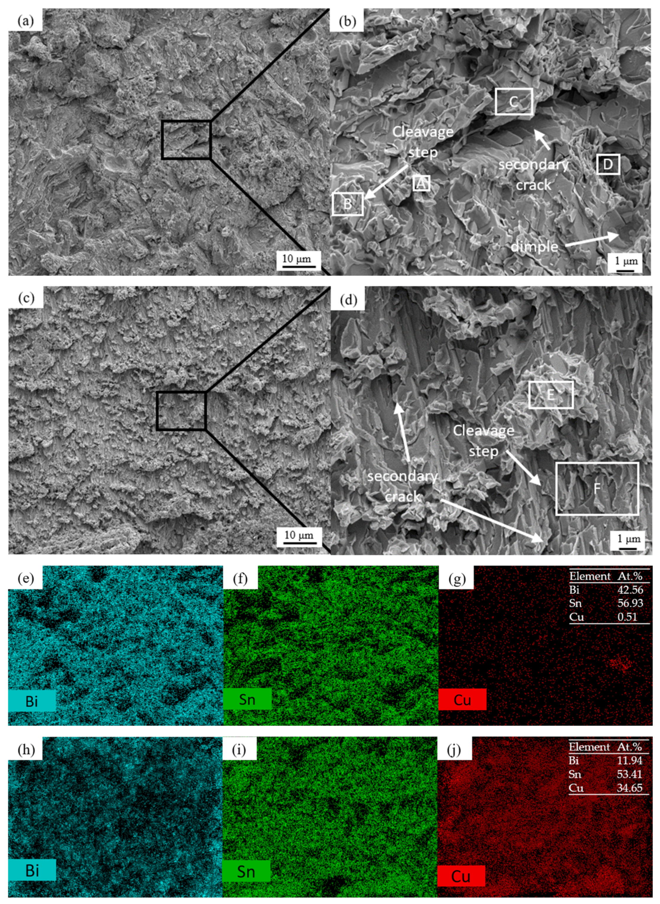
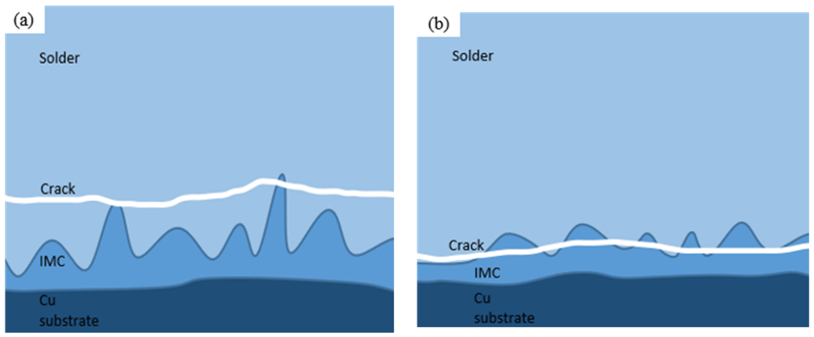
Figure 9 shows the morphology and EDS surface composition analysis results after 100 h of shear fracturing of Sn58Bi/Cu solder joints with electromigration under different joint cross-sectional areas. Figure 10 shows the schematic diagram of the fracture location of the 100 h shear fracture of Sn58Bi/Cu solder joints with electromigration under different joint cross-sectional areas, and Table 3 shows the results of the analysis of the average compositions of different regions. When the cross-sectional area of the joint is 0.25 mm2, as shown in Figure 9a,b, the shear fracture of Sn58Bi/Cu solder joints is a mixed brittle/ductile fracture dominated by the cleavage step, secondary cracks, and localized tearing ribs with a few dimples. The EDS components of Figure 9a,b were analyzed as shown in Figure 9e–g and Table 3, which revealed that the main component of the solder joint’s shear fracture area A was Sn (i.e., solder zone β-Sn phase), the main component of the area B cleavage step was Bi (i.e., solder zone Bi-rich phase), and Cu elements appeared in area D. Area D was analyzed as a transition zone composed of the Cu6Sn5 IMC and a solder zone with Sn58Bi eutectic organization, which indicated that solder joint shear fracture occurred in the solder zone near the cathode IMC layer; as shown in Figure 10a, there was a typical brittle fracture dominated by a mixed brittle/tough fracture with high joint shear strength. When the cross-sectional area of the joint is increased to 1.0 mm2, as shown in Figure 9c,d, the shear fracture of the Sn58Bi/Cu solder joint is mainly brittle fracture dominated by large-scale cleavage and accompanied by secondary cracks. The EDS composition analysis of Figure 9c,d is shown in Figure 9h–j and Table 3, from which it can be seen that the area E of the solder joint in the shear fracture shows a block organization; the main components are Sn and Bi, indicating that it is the soldering material organization. Compositional analysis of the area F cleavage step shows that it is a Cu6Sn5 IMC, which indicates that the solder joint shear fracture location has moved to the interface IMC layer, as shown in Figure 10b. This is similar to the findings of Fu et al. [44], where the fracture location of a solder joint after electromigration was concentrated in the cathode region. The joint shear strength decreased sharply to 13.4 (±2.0) MPa, which is 60.9% lower compared with the absence of electromigration.

Figure 9.
Shear fracture morphologies and EDS analysis of Sn58Bi/Cu solder joints with different cross-sectional areas after 100 h of electromigration (A-E are the EDS analysis scanning area): (a) 0.25 mm2 1000×; (b) 0.25 mm2 5000×; (c) 1.0 mm2 1000×; (d) 1.0 mm2 5000×; (e–g) Figure (a) element mapping; (h–j) Figure (c) element mapping.
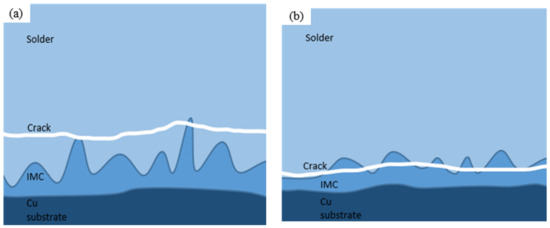
Figure 10.
Crack location in Sn58Bi/Cu solder joints with different cross-sectional areas after 100 h of electromigration: (a) 0.25 mm2; (b) 1.00 mm2.
Table 3.
EDS analysis of shear fracture of microcomponents of solder joints under different joint cross-sectional areas (At.%).
In conclusion, with the increase in the cross-sectional area of Sn58Bi/Cu solder joints, microcracks are gradually formed in the cathode area of the joints and gradually expand. The fracture mechanism of the joint shear fracture changes from a mixed brittle/tough fracture dominated by cleavage and secondary cracks to a brittle fracture dominated by cleavage, the fracture location shifts from the solder zone of the near-cathode IMC layer to the interfacial IMC layer, and the shear strength of the joint is reduced by 60.9% compared to that in the absence of electromigration.
4. Conclusions
- (1)
- With the increase in the cross-sectional area of Sn58Bi/Cu solder joints, the Joule heat and electromigration of joints increased, the anode IMC layer was thickened and transformed into a flat shape, and a Bi-rich layer was formed near the soldering zone, with its thickness gradually increasing. The cathode IMC layer first increased and then decreased and gradually dissolved; a Sn-rich zone was formed near the solder zone, and its thickness gradually increased; and microcracks were generated when the cross-sectional area of the joints was increased to 0.75 mm2.
- (2)
- With the increase in the cross-sectional area of Sn58Bi/Cu solder joints, microcracks gradually formed in the cathode area of the joints and gradually expanded. The fracture mechanism of the joint shear fracture changed from a mixed brittle/tough fracture, dominated by cleavage and secondary cracks, to a brittle fracture, dominated by cleavage; the fracture location shifted from the solder zone of the near-cathode IMC layer to the interfacial IMC layer; and the shear strength of the joint was reduced by 60.9% compared to that in the absence of electromigration.
Author Contributions
Conceptualization, Y.G. and K.Z.; methodology, Y.G.; software, C.Z. and W.C.; validation, Y.G., K.Z. and Y.W.; writing—original draft preparation, Y.G.; writing—review and editing, Y.G. and K.Z. All authors have read and agreed to the published version of the manuscript.
Funding
This research was funded by the Leading Talent in Basic Research in Central Plains (grant No. ZYYCYU202012130); the National Natural Science Foundation of China (grant No. U1604132); the Provincial and Ministerial Co-construction of Collaborative Innovation Center for Non-Ferrous Metal New Materials and Advanced Processing Technology, Henan Province, China; and the Henan International Joint Laboratory of Non-Ferrous Materials, Henan Province, China.
Data Availability Statement
The data used to support the findings of this study are included within the article.
Conflicts of Interest
The authors declare no conflict of interest.
References
- Mohd Zahri, N.A.; Yusof, F.; Ariga, T.; Haseeb, A.S.M.A.; Mansoor, M.A.; Sukiman, N.L. Open-cell copper foam joining: Joint strength and interfacial behaviour. Mater. Sci. Technol. 2019, 35, 2004–2012. [Google Scholar] [CrossRef]
- Komal, N.; Mansoor, M.A.; Mazhar, M.; Sohail, M.; Malik, Z.; Anis-ur-Rehman, M. Effect of (Sm, In) Doping on the Electrical and Thermal Properties of Sb2Te3 Microstructures. ACS Omega 2023, 8, 9797–9806. [Google Scholar] [CrossRef] [PubMed]
- Liu, P.; Guo, W.; Wu, P. Effects of GNSs addition on the electromigration of Sn58Bi and Cu-core Sn58Bi joint. J. Mater. Sci. 2022, 57, 15598–15611. [Google Scholar] [CrossRef]
- Ahmed, S.; Mansoor, M.A.; Basirun, W.J.; Sookhakian, M.; Huang, N.M.; Mun, L.K.; Söhnel, T.; Arifin, Z.; Mazhar, M. The synthesis and characterization of a hexanuclear copper–yttrium complex for deposition of semiconducting CuYO2–0.5Cu2O composite thin films. New J. Chem. 2015, 39, 1031–1037. [Google Scholar] [CrossRef]
- Daraz, U.; Ansari, T.M.; Arain, S.A.; Mansoor, M.A.; Mazhar, M. Study of solvent effect on structural and photoconductive behavior of ternary chalcogenides InBiS3-In2S3-Bi2S3 composite thin films deposited via AACVD. Main Group Met. Chem. 2019, 42, 102–112. [Google Scholar] [CrossRef]
- Bashir, M.N.; Haseeb, A.S.M.A. Grain size stability of interfacial intermetallic compound in Ni and Co nanoparticle-doped SAC305 solder joints under electromigration. J. Mater. Sci. Mater. Electron. 2022, 33, 14240–14248. [Google Scholar] [CrossRef]
- Bashir, M.N.; Haseeb, A.S.M.A.; Wakeel, S.; Khan, M.A.; Quazi, M.M.; Khan, N.B.; Ahmed, A.; Soudagar, M.E.M. Effect of Ni and Co nanoparticle-doped flux on microstructure of SAC305 solder matrix. J. Mater. Sci. Mater. Electron. 2022, 33, 20106–20120. [Google Scholar] [CrossRef]
- Ren, J.; Wang, Y.; Zhou, W.; Wang, X.; Guo, F. Effects of Sb, Bi and Ni elements on the electromigration reliability of Sn-based lead-free solder joints. Electron. Compon. Mater. 2022, 41, 641–647, 654. [Google Scholar]
- Bashir, M.N.; Butt, S.U.; Mansoor, M.A.; Khan, N.B.; Bashir, S.; Wong, Y.H.; Alamro, T.; Eldin, S.M.; Jameel, M. Role of Crystallographic Orientation of β-Sn Grain on Electromigration Failures in Lead-Free Solder Joint: An Overview. Coatings 2022, 12, 1752. [Google Scholar] [CrossRef]
- Wang, F.; Chen, H.; Huang, Y.; Liu, L.; Zhang, Z. Recent progress on the development of Sn–Bi based low-temperature Pb-free solders. J. Mater. Sci. Mater. Electron. 2019, 30, 3222–3243. [Google Scholar] [CrossRef]
- Wang, S.; Tian, Y. The state of art on the micro-joining and nano-joining technologies. Mater. Sci. Technol. 2017, 25, 1–5. [Google Scholar]
- Xu, J.; Cai, C.; Pham, V.; Pan, K.; Wang, H.; Park, S. A Comprehensive Study of Electromigration in Lead-free Solder Joint. In Proceedings of the 2020 IEEE 70th Electronic Components and Technology Conference (ECTC), The Cosmopolitan of Las Vegas, Las Vegas, NV, USA, 26–29 May 2020. [Google Scholar]
- Tu, K.N. Recent advances on electromigration in very-large-scale-integration of interconnects. J. Appl. Phys. 2003, 94, 5451–5473. [Google Scholar] [CrossRef]
- Pan, Y.; Zhang, K.; Zhang, C.; Wang, H.; Li, J.; Zhong, S. Effect of Electromigration on Microstructure and Properties of Ni-rGO Reinforced Sn2.5Ag0.7Cu0.1RE Composite Solder/Cu Soldering Joints. J. Henan Univ. Sci. Technol. (Nat. Sci.) 2020, 41, 5–11+117–118. [Google Scholar]
- Jiang, N.; Zhang, L.; Gao, L.-L.; Song, X.-G.; He, P. Recent advances on SnBi low-temperature solder for electronic interconnections. J. Mater. Sci. Mater. Electron. 2021, 32, 22731–22759. [Google Scholar] [CrossRef]
- Alford, T.L.; Misra, E.; Bhagat, S.K.; Mayer, J.W. Influence of Joule heating during electromigration evaluation of silver lines. Thin Solid Film. 2009, 517, 1833–1836. [Google Scholar] [CrossRef]
- Zhao, W.S.; Zhang, R.; Wang, D.W. Recent Progress in Physics-Based Modeling of Electromigration in Integrated Circuit Interconnects. Micromachines 2022, 13, 883. [Google Scholar] [CrossRef] [PubMed]
- Bashir, M.N.; Khan, N.B.; Bashir, S.; Khan, A.F.; Quazi, M.M.; Gul, M.; Wakeel, S.; Saad, H.M. Effect of Zn nanoparticle-doped flux on mechanical properties of SAC305 solder joint after electromigration. J. Mater. Sci. Mater. Electron. 2023, 34, 321. [Google Scholar] [CrossRef]
- Murayama, K.; Kurihara, T.; Sakai, T.; Imaizumi, N.; Shimizu, K.; Sakuyama, S.; Higashi, M. Electro-migration Behavior in Eutectic Sn-Bi Flip Chip Solder Joints with Cu-Pillar Electrodes. J. Smart Process. 2013, 2, 178–185. [Google Scholar] [CrossRef]
- Nguyen, H.V.; Salm, C.; Krabbenborg, B.H.; Bisschop, J.; Mouthaan, A.J.; Kuper, F.G. Fast Thermal Cycling-Enhanced Electromigration in Power Metallization. IEEE Trans. Device Mater. Reliab. 2004, 4, 246–255. [Google Scholar] [CrossRef]
- Cui, H.; Liu, X.; Deng, D. Influence factors for electromigration of metal interconnects. Trans. China Weld. Inst. 2018, 39, 29–32+130. [Google Scholar]
- Wang, F.; Liu, L.; Li, D.; Wu, M. Electromigration behaviors in Sn–58Bi solder joints under different current densities and temperatures. J. Mater. Sci. Mater. Electron. 2018, 29, 21157–21169. [Google Scholar] [CrossRef]
- Basaran, C.; Abdulhamid, M.F. Low temperature electromigration and thermomigration in lead-free solder joints. Mech. Mater. 2009, 41, 1223–1241. [Google Scholar] [CrossRef]
- Gu, X.; Yang, D.; Chan, Y.C.; Wu, B.Y. Effects of electromigration on the growth of intermetallic compounds in Cu/SnBi/Cu solder joints. J. Mater. Res. 2011, 23, 2591–2596. [Google Scholar] [CrossRef]
- Xu, G.; He, H.; Guo, F. Temperature-Dependent Phase Segregation in Cu/42Sn-58Bi/Cu Reaction Couples under High Current Density. J. Electron. Mater. 2008, 38, 273–283. [Google Scholar] [CrossRef]
- Guo, F.; Liu, Q.; Ma, L.; Zuo, Y. Diffusion behavior of Sn atoms in Sn58Bi solder joints under the coupling effect of thermomigration and electromigration. J. Mater. Res. 2016, 31, 1793–1800. [Google Scholar] [CrossRef]
- Ouyang, F.Y.; Tu, K.N.; Lai, Y.S. Effect of electromigration induced joule heating and strain on microstructural recrystallization in eutectic SnPb flip chip solder joints. Mater. Chem. Phys. 2012, 136, 210–218. [Google Scholar] [CrossRef]
- Chiu, S.H.; Shao, T.L.; Chen, C.; Yao, D.J.; Hsu, C.Y. Infrared microscopy of hot spots induced by Joule heating in flip-chip SnAg solder joints under accelerated electromigration. Appl. Phys. Lett. 2006, 88, 022110. [Google Scholar] [CrossRef]
- Nah, J.W.; Suh, J.O.; Tu, K.N. Effect of current crowding and Joule heating on electromigration-induced failure in flip chip composite solder joints tested at room temperature. J. Appl. Phys. 2005, 98, 013715. [Google Scholar] [CrossRef]
- Xu, G.C.; Guo, F.; Zhu, W.R. Electromigration in eutectic SnAg solder reaction couples with various ambient temperatures and current densities. Int. J. Miner. Metall. Mater. 2009, 16, 685–690. [Google Scholar]
- Feng, D.D.; Wang, F.J.; Li, D.Y.; Wu, B.; Liu, L.T. Atomic migration on Cu in Sn-58Bi solder from the interaction between electromigration and thermomigration. Mater. Res. Express 2019, 6, 046301. [Google Scholar] [CrossRef]
- Shen, Y.-A.; Zhou, S.; Nishikawa, H. Preferred orientation of Bi and effect of Sn-Bi microstructure on mechanical and thermomechanical properties in eutectic Sn-Bi alloy. Materialia 2019, 6, 100309. [Google Scholar] [CrossRef]
- Dong, W.; Shi, Y.; Xia, Z.; Lei, Y.; Guo, F. Effects of Trace Amounts of Rare Earth Additions on Microstructure and Properties of Sn-Bi-Based Solder Alloy. J. Electron. Mater. 2008, 37, 982–991. [Google Scholar] [CrossRef]
- Zhang, C.; Zhang, K.; Gao, Y.; Wang, Y. Study on Microstructure and Mechanical Properties at Constant Electromigration Temperature of Sn2.5Ag0.7Cu0.1RE0.05Ni-GNSs/Cu Solder Joints. Materials 2023, 16, 2626. [Google Scholar] [CrossRef] [PubMed]
- Liu, C.; Zhang, W.; Sui, M.; Shang, J. Bi segregation at interface of the eutectic SnBi/Cu solder joint. Acta Metall. Sin. 2005, 41, 847–852. [Google Scholar]
- Chen, J.; Wang, J.; Zhang, Z.; Zhang, P.; Yu, Z.; Yu, C.; Lu, H. Advances in Metallurgical Behavior of Micro/nano-scale Cu-Sn Interface. J. Mech. Eng. 2022, 58, 223–235. [Google Scholar]
- Huang, J.; Wang, X.; Chen, J.; Wei, W.; Liu, F.; Qin, B.; Wang, H.; Zhang, Y. Growth mechanisms of intermetallic compounds and Bi-rich layer in ball grid array structure Cu/Sn-58Bi/Cu solder joints during solid-solid and liquid-solid electromigration. J. Mater. Sci. Mater. Electron. 2022, 33, 10297–10313. [Google Scholar] [CrossRef]
- Jose, S. Package-level Joule-heating measurements for multilevel interconnects. Microelectron. Reliab. 2022, 138, 114767. [Google Scholar] [CrossRef]
- Li, S.; Zhang, K.; Zhang, C.; Li, J.; Wu, W. Microstructure and Properties of Ni-GNSs Reinforced Sn2.5Ag0.7Cu0.1RE Composite Solder/Cu Soldering Joint during Thermal Migration. J. Henan Univ. Sci. Technol. (Nat. Sci.) 2022, 43, 1–6+117. [Google Scholar]
- Chen, L.; Tan, S.X.D.; Sun, Z.; Peng, S.; Tang, M.; Mao, J. A Fast Semi-Analytic Approach for Combined Electromigration and Thermomigration Analysis for General Multisegment Interconnects. IEEE Trans. Comput. Aided Des. Integr. Circuits Syst. 2021, 40, 350–363. [Google Scholar] [CrossRef]
- Shen, X.; Kwak, S.L.; Jeong, W.H.; Jang, J.W.; Yu, Z.; Ahn, H.; Park, H.J.; Choi, H.; Park, S.H.; Snaith, H.J.; et al. Thermal Management Enables Stable Perovskite Nanocrystal Light-Emitting Diodes with Novel Hole Transport Material. Small 2023, in press. [Google Scholar] [CrossRef]
- Pang, X.; Liu, Z.; Wang, S.; Shang, J. First-principles calculations of doped elements on electromigration of Bi. Chin. J. Nonferrous Met. 2011, 21, 875–881. [Google Scholar]
- Li, Y.; Li, X.; Yao, P. Effect of vacancy on the elements diffusion in Cu/Sn leadfree solder joints. Trans. China Weld. Inst. 2018, 39, 25–30+130. [Google Scholar]
- Fu, Z.W.; Chen, J.; Zhao, P.F.; Guo, X.T.; Xiao, Q.Z.; Fu, X.; Wang, J.; Yang, C.; Xu, J.L.; Yang, J.Y. Interfacial Reaction and Electromigration Failure of Cu Pillar/Ni/Sn-Ag/Cu Microbumps under Bidirectional Current Stressing. Materials 2023, 16, 1134. [Google Scholar] [CrossRef]


Disclaimer/Publisher’s Note: The statements, opinions and data contained in all publications are solely those of the individual author(s) and contributor(s) and not of MDPI and/or the editor(s). MDPI and/or the editor(s) disclaim responsibility for any injury to people or property resulting from any ideas, methods, instructions or products referred to in the content. |
© 2023 by the authors. Licensee MDPI, Basel, Switzerland. This article is an open access article distributed under the terms and conditions of the Creative Commons Attribution (CC BY) license (https://creativecommons.org/licenses/by/4.0/).