Abstract
AlCrSiN coatings are promising protective candidates for cutting and forming tools. During the coating deposition process, the microstructure and properties of the coatings were dramatically affected by bias voltages. To further optimize and enhance the AlCrSiN coating, a series of coatings were deposited at different pulse bias voltages using arc ion plating technology. By virtue of scanning electron microscopy, X-ray diffraction, scratch method, OCP, EIS, and other analytical methods, the effects of the pulse bias voltage on the crystal structure, microstructure, and mechanical, tribological, and electrochemical properties of the AlCrSiN coatings were analyzed. The study revealed that the pulse bias voltage exerted a slight influence on the aluminum and nitrogen content of the coatings. As the pulse bias voltage increased, the hardness, critical load, and tribological performance of the AlCrSiN coatings first increased gradually, and then were impaired slightly. When the pulse bias voltage was −100 V, the resulting AlCrSiN coating exhibited the densest structure, the highest hardness, the strongest adhesion, and the best wear resistance. In this case, the coating hardness and critical load reached 2668 HV and 72.7 N, respectively. The friction coefficient and wear rate were 0.35 and 1.02 × 10⁻³ μm3/N·μm, respectively. Simultaneously, the AlCrSiN coating demonstrated exceptional corrosion resistance in 3.5 wt.% NaCl solutions, surpassing uncoated 304 steel by 3~4 times.
1. Introduction
AlCrN coatings have garnered increasing attention owing to their excellent properties, such as high hardness, superior tribological properties, and superior oxidation resistance, making them highly promising for applications in cutting and forming tools [1,2]. In order to further enhance the thermal stability and toughness of AlCrN coatings, Si-containing AlCrSiN coatings with a nanocomposite structure have been developed. This nanocomposite structure of AlCrSiN impedes grain growth at elevated temperature, thereby improving the overall thermal stability [3]. However, it is important to note that the characteristics and properties of these coatings are strongly influenced by various factors, such as deposition processes, deposition parameters, chemical composition, substrates, and more [4,5].
Currently, numerous researchers have endeavored to enhance the properties of Si-containing coatings by regulating the deposition parameters. It has been previously reported that by increasing the aluminum and silicon contents, the crystal direction of AlCrSiN coatings changes from (111) to (100), and the degree of anisotropy decreases with higher aluminum content [6]. Additionally, Li et al. [7] reported that varying the N2/Ar flow ratio leads to a gradual transformation of nanocrystals in the AlCrSiN coating from a metastable solution fcc-(Cr, Al)N phase to a mixed fcc-(Cr, Al)N and hcp-(Cr, Al)N phase. This transformation enhances the coating’s crystallinity, resulting in increased hardness and elastic modulus. Moreover, Si-containing AlCrSiN coatings exhibit a nanocomposite structure wherein nanocrystalline grains are dispersed in an amorphous α-SiNx matrix, contributing to the augmentation of interfacial phase and refinement of crystals [8]. Among all the deposition parameters, the bias voltage is one of the most crucial factors influencing the microstructures and the mechanical and tribological characteristics of the coatings [9]. During the coating deposition process, the application of substrate bias generates a plasma formed by evaporation and ionization of the target material, which is then accelerated and redeposited on the negatively charged substrate in the electric field. Pulse bias plays a significant role in ion implantation, etching, film formation, and stress relief. Notably, Fan et al. [10] demonstrated that altering the bias voltage resulted in a shift of CrN preferred orientations from (200) to (220) and facilitated the formation of the Cr2N phase. Furthermore, an increase in bias voltage effectively reduced the presence of microparticles on the coating surface. As observed by Cai [11], higher pulse bias voltage led to decreased friction coefficient and wear rate of AlTiSiN coatings.
Despite the considerable research on AlCrSiN coatings, the impact of pulse bias voltage on their properties has received limited attention. To gain deeper insights into the underlying mechanism of bias voltage on the microstructure and properties of AlCrSiN coatings, a series of AlCrSiN coatings with varying bias voltages were deposited by arc ion plating technology. The primary objectives of this study were to identify optimal process parameters and to investigate the influence of bias voltage on the microstructure, mechanical properties, tribological behaviors, and corrosion resistance of the above coatings.
2. Materials and Methods
2.1. Coating Deposition
The AlCrSiN coatings were deposited using automatic arc ion plating machine (AIP 650/750, Dalian Vacuum Technologies, Dalian, China) at various pulse bias voltages (0 V, −50 V, −100 V, −200 V, −300 V) on (100) Si wafers (50 × 10 × 0.67 mm3), polished cemented carbide (25 × 25 × 3 mm3), and SUS 304 stainless steel (20 × 20 × 1 mm3) substrates. The utilization of Si substrate enables a thorough characterization of coating composition and microstructure, thereby providing crucial data on elemental distribution and phase identification within the coatings. In parallel, the adoption of SUS 304 stainless steel substrate facilitates precise evaluation of the coating’s corrosion performance, owing to the susceptibility of this steel grade to corrosion under specific environmental conditions. Before deposition, the samples were meticulously cleaned in an ultrasonic machine with degreaser, ultrapure water, and alcohol for 15 min each. Subsequently, the substrates were dried and fixed on rotating substrate holders at a speed of 30 Hz during the deposition process. For the preparation of AlCrSiN coatings, pure metal Cr (99.99%) target and an AlCrSi alloy target (φ100 × 25 mm, Al:Cr:Si = 60:30:10, 99.9% purity) were employed. The working and reaction gases were Ar (99.999% purity) and N2 (99.999% purity), respectively. To ensure a clean substrate surface, a plasma etching procedure was conducted using Ar glow discharge at a DC bias of −800 V for 20 min. Subsequently, ion bombardment was performed by the Cr target for 8 min, reducing the DC bias from −800 to −600, −400, and −200 V at 2 min intervals, thereby effectively removing any remaining contaminants from the substrate surface. During the coating deposition, the working pressure was maintained at 0.6 Pa. Initially, a Cr transition layer was deposited at a pulse bias voltage of −100 V for 10 min, with a pulse frequency and pulse width of 50 kHz and 8 μs, respectively, and the duty ratio is 60%. Subsequently, the functional coating was applied under specific conditions of a total gas flow of N2 and Ar kept constant at 190 mL/min, with a pulse frequency and pulse width of 50 KHz and 6 μs, respectively, a duty ratio of 70%, and a pulse bias voltage applied to the substrates that ranged from 0 to −300 V. The deposition time for the AlCrSiN coatings was 180 min. Detailed deposition parameters are provided in Table 1.

Table 1.
Detailed deposition parameters for the AlCrSiN coatings.
2.2. Characterization of Coatings
Surface and cross-section images of all the coatings were acquired using a field emission scanning electron microscope (FE-SEM, Hitachi S-4800, Tokyo, Japan), and their chemical composition was determined using energy dispersive spectroscopy (EDS) integrated with FESEM. Phase analysis of the coatings was performed using an X-ray diffractometer (XRD, Brucker D8-Discovery, Mannheim, Germany) equipped with Cu Kα radiation (λ = 0.15418 nm). The spectra were recorded at a scanning rate of 6°/min over diffraction angles ranging from 20° to 80° (2θ).
The hardness of the coating was measured in accordance with ISO 4516 standard, utilizing a microhardness tester (Wilson 402MVD, Norwood, MA, USA). The test involved pressing a 130° diamond pyramidal indenter into the coating’s surface under a specified load. A pit was formed on the surface, and the length of the diagonal line of the pit was measured using an eyepiece micrometer. Equation (1) was then employed to calculate the microhardness value of the coating. A load of 25 mN was applied with a dwelling time of 10 s, and a minimum of 10 indents were made on each coating to obtain an average value and reduce error.
where HV represents the Vickers hardness, P denotes the load weight, and d corresponds to the diagonal length of the pit.
HV = 18.18 · P/d2
To assess the adhesion strength between the coating and the substrate, the ISO 20502 standard was followed using a scratch tester (Anton Paar RST-3, Graz, Austria). A spherical diamond tip with a diameter of 200 µm was utilized to scratch the coating surface, gradually increasing the load from 0 N to 150 N. The scratch length was fixed at 5 mm, and the loading rate was 5 N/s with a scratch speed of 10 mm/min. To ensure accuracy, each sample underwent three tests, and the average value of the results was considered as the critical load of the coating.
The friction and wear behavior of AlCrSiN coatings were evaluated using a high temperature ball-on-disk tribometer (Anton Paar THT, Graz, Austria) under ambient conditions. The test parameters included a load of 2 N, a speed of 30 Hz, and Al2O3 balls with 6 mm diameters as the grinding counterpart. The tribological tests were conducted continuously for a duration of 131.95 m, with real-time monitoring of the friction coefficient recorded using the computer. The worn surface of the coatings was examined using a super-wide depth of field microscope (Keyence VHX-1000C, Osaka, Japan). The depth and cross-section area of the wear scar were quantified using an Alpha Step D Series Probe Profiler. The specific wear rate (W) was determined utilizing Archard’s classical Equation (2):
where V represents the wear volume, and L and S denote the applied load and the total sliding distance, respectively.
W = V/L × S
The electrochemical properties of AlCrSiN coatings were investigated using a classical three-electrode cell in a Zennium X electrochemical workstation. For these experiments, 304 steel samples served as the working electrodes, while a Ag/AgCl electrode and a platinum electrode were utilized as the reference and auxiliary electrodes, respectively. Each electrochemical test was conducted at least three times to ensure reproducibility. The working electrode was held at the open circuit potential (OCP) for 1 h to reach a stable state. Electrochemical impedance spectroscopy (EIS) was conducted using an AC signal with an amplitude of 10 mV at OCP, over a frequency range of 10 mHz~10 kHz.
3. Results
3.1. Chemical Composition and Phase Analysis
Figure 1 presents the EDS analysis of the chemical composition of AlCrSiN coatings at different pulse bias voltages. The results indicate that as the pulse negative bias of 126 voltages increased from 0 V to −300 V, Al content and Cr content changed from 36.19 at.% and 19.82 at.% to 39.67 at.% and 16.81 at.%, respectively. This behavior can be attributed to the lighter nature of Al atoms compared to Cr atoms, making them more susceptible to heavy sputtering at higher bias voltage. This observation is consistent with previous studies by Tang et al. [12], which demonstrated a decrease in aluminum content with an increase in bias voltage. Higher pulse bias voltages result in enhanced excitation and collision probability of Al atoms, leading to higher sputtering rates [13]. The Si and N contents, on the other hand, remained relatively consistent with the increase in bias voltage, peaking at −100 V, and then decreasing, indicating a reduction in the amorphous Si3N4 component in the coatings. Moreover, the presence of negative bias induced varying degrees of anti-sputtering effect, leading to a reduced deposition rate of Si and Cr nitrides and consequently lowering their content in the coatings. Overall, the findings suggest that pulse bias voltage has limited influence on the chemical composition of AlCrSiN coatings deposited by arc ion plating.
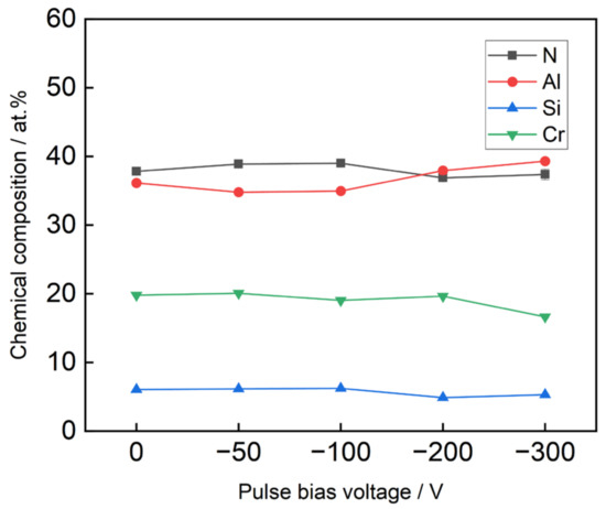
Figure 1.
Compositions of the AlCrSiN coatings deposited at different pulse bias voltages.
Figure 2 illustrates the XRD diffraction patterns of the AlCrSiN coatings prepared at different bias voltages. As anticipated, the diffraction patterns exhibited a combination of bcc-AlN (PDF #70-0354), fcc-AlN (PDF #80-0010), and fcc-CrN (PDF #76-2494) phases across all five sets of coatings. When the pulse negative bias was not applied, the coating displayed strong bcc-AlN diffraction peaks along the (100), (002), and (110) crystal planes, along with weak fcc-CrN diffraction peaks along (200) crystal planes. As the pulse negative bias voltage increased from 0 to −100 V, the diffraction peaks of the bcc-AlN phase growing along the (100) and (002) crystal planes gradually weakened, while those along the (110) crystal plane increased, with the intensity reaching its maximum at 2θ = 58.52°. This behavior can be attributed to the formation of the amorphous Si3N4 phase in the coating, which hinders grain growth within the coating. Upon further increase in the substrate negative bias to −300 V, the diffraction peak of the (100) crystal plane strengthened, while that of the (110) crystal plane weakened. A weak peak of the fcc-CrN diffraction peaks was detected in the coatings deposited at −100 V bias voltage, while the fcc-CrN diffraction peak broadened and shifted to small angles in the films deposited at −200 V and −300 V bias. This phenomenon might be attributed to a tendency for phase separation into fcc-CrN domains at −100 V bias voltages, which is not observed at lower bias voltages. Additionally, all diffraction peaks slightly shifted to lower angles and broadened, indicative of increasing growth stress in the coating due to stronger ion bombardment effect [14]. Furthermore, due to the solid solution formed by some Cr atoms with a smaller atomic radius (0.127 nm) replacing Al atoms with a larger atomic radius (0.143 nm), no distinct diffraction peaks of the CrN phase were detected [15]. The small amount of Cr dissolved in the AlN lattice causes AlN lattice distortion, resulting in an increased lattice constant and a shift of the AlN phase diffraction peak to smaller angles. As the bias voltage increased, the evaporated ions gained greater energy and strongly bombarded the deposited coatings, which lead to the greater lattice distortions and an increased number of defects. In the XRD pattern (Figure 2), no diffraction peaks of SiNx were observed, indicating that the SiNx phase in the coating exists in an amorphous state, thus forming the hard nano-crystallites of the AlN phase surrounded by thin amorphous states, thereby forming a nanocomposite structure [16].
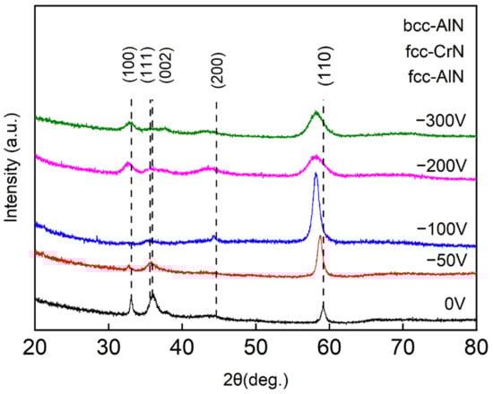
Figure 2.
XRD patterns of the AlCrSiN coatings deposited at different pulse bias voltages.
3.2. Morphologies
Figure 3 depicts the surface morphology of AlCrSiN coatings prepared at different pulse bias voltages, observed using SEM, where Figure 3a–e correspond to the pulse bias voltages of 0 V, −50 V, −100 V, −200 V, and −300 V. It is evident that the surfaces of all these coatings exhibit significant roughness and contain various defects, such as macroparticles, droplets, and pits. As the pulse bias voltage increases, the number of particles and droplets on the coating surface initially decreases and then increases, with the minimum number and size of particles observed at a pulse bias voltage of −100 V. These particles and droplets primarily result from the unstable motion of the arc spot on the target surface at high temperature, leading to energy dispersion and changes in plasma density, and particles evaporated from the target surface are directly deposited on the substrate surface. However, when a bias voltage is applied to the substrate, a negative electric field is established. Under the higher bias voltages, accelerated particles gained higher kinetic energy, leading to more intense collisions and enhanced removal of larger particles. Additionally, the effect of electrostatic repulsion within the near-substrate plasma sheath also affects the number of microparticles on the coating surface. It has been reported that in the process of physical vapor deposition, the evaporated particles underwent random collisions with electrons, ions, or neutral atoms, absorbing them in the process [17]. These collisions alter the macroscopic particle’s charge state. Due to the significant mass difference between electrons and ions, electrons’ charge effect dominates over ions, resulting in a net negative charge being generated on the surface of large particles. Consequently, a substrate biased with a negative voltage will exert repulsive forces on approaching particles, leading to a reduction in microparticles. Moreover, an increase in the bias voltage enhanced the repulsive effect. However, when the pulse bias voltage is increased beyond −200 V, a significant increase in the number of particles on the coating surface were observed. This phenomenon can be attributed to the fact that higher bias voltage increases the ion energy, causing reverse sputtering of the coating surface. Low fluxes at high energies lead to renucleation, growth disruption, and structure damage, whereas high fluxes at relatively low energies promote adatom mobility and continuous crystal growth [18]. Additionally, the substrate temperature may rise with increasing bias voltage, which could also contribute to the deterioration of the coating’s surface structure.
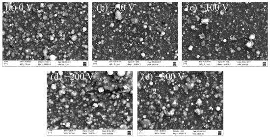
Figure 3.
Surface morphologies of the AlCrSiN coatings deposited at different pulse bias voltages. (a) 0 V; (b) −50 V; (c) −100 V; (d) −200 V; (e) −300 V.
The cross-sectional morphologies of AlCrSiN coatings deposited at different pulse biases are shown in Figure 4. It is evident that all coatings exhibit a well-bonded interface with the substrate and lack an obvious columnar structure, which can be attributed to the influence of Si on the coating’s columnar growth. Without any applied bias, the coating structure appears loose, and the cross-section reveals holes formed by droplet shedding. As the negative bias is increased to −50 V, the coating structure becomes denser, but the boundary between the CrN transition layer and the AlCrSiN coating remains less distinct. This observation is mainly due to the increased kinetic energy of the incident ions following the application of the bias voltage, leading to densification of the coating’s structure and a smoother surface through ion bombardment. At a negative bias voltage is −100 V, the interface between the coating and the transition layer becomes more evident, and the structure becomes more dense. Increasing the bias voltage induces a reverse sputtering effect, which effectively bombards larger particles suspended on the coating surface resulting in a refinement of the coating structure [19]. This observation aligns with the XRD analysis, as an increase in negative bias leads to aggravated lattice distortion and grain refinement. Additionally, the presence of an amorphous phase in the coating inhibits grain growth, increases the grain boundary area, and obstructs grain boundary slip and microcrack expansion, all of which contribute to a denser coating cross-section [20]. However, as the bias voltage is further increased, uneven bonding between the transition layer and the substrate, along with the presence of large particles embedded in the coating, is observed. This phenomenon arises from excessively high bias voltages exacerbating the reverse sputtering effect and elevating the internal stress within the coating. Consequently, cracking or even peeling off of the coating may occur, consistent with findings reported by Fan et al. [10].
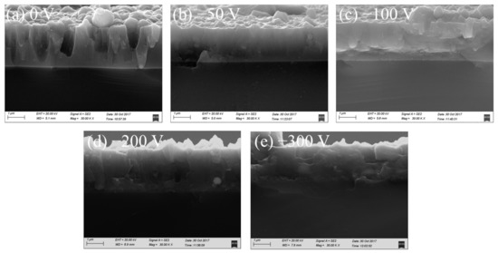
Figure 4.
Cross-sectional morphologies of the AlCrSiN coatings deposited at different pulse bias voltages. (a) 0 V; (b) −50 V; (c) −100 V; (d) −200 V; (e) −300 V.
3.3. Microhardness and Critical Load
Figure 5 illustrates the microhardness of the AlCrSiN coatings prepared at different pulse bias voltages. The results demonstrate a non-linear relationship between hardness and pulse bias voltage, with the hardness initially increasing and then decreasing. Notably, the coating prepared at −100 V achieves the highest hardness of 2668 MPa. The coating deposited without any bias voltage exhibits a loose and discontinuous microstructure (Figure 4a) containing numerous microparticles and displaying relatively low hardness. The increase in hardness observed when pulsed negative bias voltage increases from 0 to −100 V and can be primarily attributed to the grain boundary hardening phenomenon caused by the strong binding energy of grain boundaries [21,22]. As the bias voltage is increased, the coating structure becomes more continuous and compact, leading to an increase in compressive stress and residual stress, which, in turn, contributes to the increased hardness. Higher bias voltage results in greater bombardment energy of incident particles on the substrate, leading to increased internal stress and higher coating hardness [23]. As reported in the literature [24], higher bias voltage leads to a greater amount of evaporated ions+ attracted from the cathode to the substrate, increasing their kinetic energy and resulting in a denser coating with higher compressive stress and hardness. The XRD analysis suggests that with increasing negative bias on the substrate, ceramic AlN phases with multiple orientations, grain refinement, and nanocomposite structure due to a-Si3N4, along with the solid solution strengthening effect of (Al, Cr)N phase, all contribute to the improvement of coating hardness [25]. Nonetheless, excessively high substrate negative bias may impede the amplitude modulation decomposition effect on the fcc-(Al, Cr)N phase in the Al-Cr-Si-N coating, thereby reducing the hardness of the coating [26].
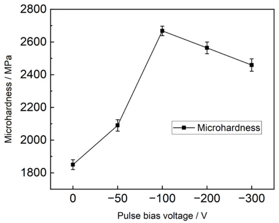
Figure 5.
Microhardness of the AlCrSiN coatings deposited at different pulse bias voltages.
The bonding strength between the AlCrSiN coating and the substrate was characterized using a scratch test, and the scratch morphology of the coatings at a pulse bias voltage of −100 V is shown in Figure 6. The scratch process of the coatings can be generally divided into three stages: the microcracks initiation stage (critical load is represented by Lc1), where the coating still remains effective despite the presence of microcracks; the local peeling stage (critical load is represented by Lc2), during which the coating’s functionality begins to be affected, and partial delamination and flaking occur; and the complete peeling stage (critical load is represented by Lc3), where the substrate is completely exposed, indicating complete coating exfoliation. The second stage is typically defined as a sign of coating adhesion failure and represents the adhesive strength of the coating. Figure 7 illustrates the critical load of the coatings at different pulse bias voltages. It can be observed that the critical load of the coatings increased first and then decreased with increasing bias voltage. The coating prepared without bias applied to the substrate exhibits the lowest critical load of 62.8 N. In this case, ions were freely deposited on the surface of the substrate, making microcracks more prone to occur and propagate along the surface and defects, leading to rapid coating failure. On the other hand, the highest adhesive strength of the coating is obtained at a pulse bias voltage of −100 V, reaching 72.7 N. Several factors contribute to this improvement. The first reason is that the coating structure under this condition possesses high density, leading to improved adhesive strength, as shown in Figure 4. Moreover, the use of arc ion plating technology releases high-energy particles to bombard the surface of the substrate, which can form a clean and superior chemical bonding interface between the coating and substrate surface, effectively improving the adhesion strength. Additionally, slight differences in grain size distribution or local epitaxial growth caused by different precipitations of the substrate variants may be another reason [27]. However, as the bias voltage is further increased, the critical load decreases. The research by Fan et al. [10] reported that the residual stress gradually decreases with an increase in the bias voltage, as high residual stress can accelerate the cracking and peeling of the coating, which aligns with the experimental results.

Figure 6.
Scratch morphology of the AlCrSiN coatings deposited at −100 V pulse bias voltage.
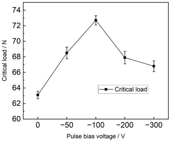
Figure 7.
Critical load of the AlCrSiN coatings deposited at different pulse bias voltages.
The aforementioned results demonstrate that increasing the pulse bias voltage can enhance the adhesive strength of the coating by promoting the coating surface and improving the structure and the density of the coating. However, it is noteworthy that further increasing the bias voltage leads to a reduction in the adhesive strength of the coating. The pulse bias voltage operates in two working states: working hours and idle hours. The application of a high pulse bias voltage during working hours significantly elevates the local temperature of the substrate compared to the lower temperature during idle hours. This temperature difference results in substantial thermal stress accumulation within the coating. These accumulated stresses are susceptible to generating cracks when subjected to external load, consequently leading to a decrease in the adhesive strength of the coating.
3.4. Tribological Properties
The average friction coefficients for the five sets of AlCrSiN coatings are presented in Figure 8 and Figure 9, respectively, revealing a strong dependency of friction behavior on the pulse bias voltage. Figure 8 illustrates that the friction pair initially undergoes a running-in state, with the friction coefficient increasing rapidly, typically attributed to the interaction between the surface oxide layer and the Al2O3 ball. Subsequently, a relatively steady state is reached, representing the frictional force within the coating. The trend of the friction coefficient is consistent with reported by Polcar et al [28]. Notably, the coatings deposited at pulse bias voltages of −50 V and −100 V exhibit exceedingly smooth friction curves, while slight fluctuations are observed in the friction curves of coatings deposited at other pulse biases. This observation is consistent with the SEM images of the coating surface, indicating a potential correlation with the presence of numerous microparticles on the coating surface. During repeated friction, wear debris formed by partial peeling at the wear scar could cause significant fluctuations in the friction coefficient. However, the large particles distributed at the edge of the wear scar may also influence the stability of friction.
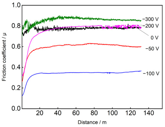
Figure 8.
Friction coefficients of the AlCrSiN coatings deposited at different pulse bias voltages.
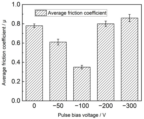
Figure 9.
Average friction coefficients of the AlCrSiN coatings deposited at different pulse bias voltages.
As shown in Figure 9, the friction coefficient of the AlCrSiN coatings gradually decreases from 0.78 to its lowest value of 0.35 as the pulse bias voltage increases from 0 to −100 V. This decrease in friction coefficient can be attributed to the strengthened ion bombardment during deposition, which enhances the density of the coatings and leads to the formation of a central cubic structure AlN within the coating [29]. The high density and the presence of a face-centered cubic structure in the coating contribute to reducing the friction coefficient. However, with a further increase in pulse bias voltage beyond −100 V, the friction coefficients of the AlCrSiN coatings start to increase. In this case, the dense structure of the coating is damaged due to the high-energy ion bombardment, and the excessive pulse bias voltage may lead to an increase in internal growth stress and thermal stress, both of which contribute to an increase in the friction coefficient [30].
Figure 10 illustrates the wear rate of the AlCrSiN coatings deposited at different pulse bias voltages. The wear resistance of coatings exhibits a gradual and subsequent significant weakening as the bias voltages increase. Notably, the wear rate is minimized at a pulse bias voltage of −100 V, reaching 1.02 × 10⁻³ μm3/N·μm, indicating the highest wear resistance at this condition. Conversely, the wear rate reaches its maximum value of 9.56 × 10⁻³ μm3/N·μm when the pulse bias voltage is −300 V. These findings are consistent with the changing trends observed for the friction coefficient, microstructure, and mechanical properties. In addition, combined with the results of XRD pattern analysis, when the negative bias of the substrate is −100 V, the appearance of polymorphic (bcc-AlN and fcc-AlN) AlN phases further improves its wear resistance [31].
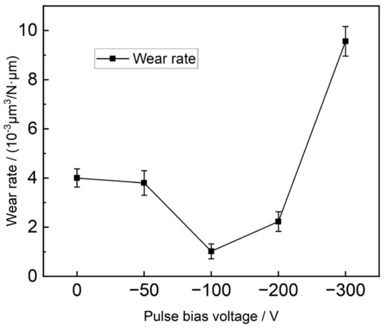
Figure 10.
Wear rate of the AlCrSiN coatings deposited at different pulse bias voltages.
The worn morphology of the coating under different bias voltages is illustrated in Figure 11. Irregular debris layers are observed across the worn surface, indicating abrasive wear as the predominant wear mechanism. During the initial wear process, hard particles and fragments stripped from the coating and friction pair act as the third body, causing micro furrow wear on the friction interface. A similar wear mechanism was also discussed by Wang et al. [30]. Upon careful examination, it is evident that when the pulse bias voltage is −100 V, the coating exhibits the narrowest wear scar width and the smoothest wear scar surface with the least debris around it. This indicates that the coating experiences minimal wear. Notably, the friction coefficient and wear rate change curves of these samples are consistent with these findings. Conversely, at bias voltages of 0 V and 300 V, the coatings show wider wear scars with more debris and rougher surfaces, indicating a higher wear rate. During the friction process, the contact surface of the friction pair is partially adhered due to atomic bonding, which leads to the formation of wear debris after some of the adhered points fall off during the subsequent sliding, which is distributed on the edge of the wear scar. The difference in hardness and critical load for the coatings deposited at these bias voltages may contribute to the varying wear behavior. For coatings deposited at a bias voltage of 0 V with a lower critical load and hardness values, they are more prone to peel off and produce wear debris. The soft abrasives then adhere to the grinding ball’s surface, exacerbating the coating wear. On the other hand, coatings deposited at a bias voltage of 300 V exhibit higher critical load and hardness, but they experience more severe wear. This could be attributed to the reverse sputtering effect produced by the high ion energy, leading to decreased wear resistance. Moreover, the sliding wear test mainly concentrates on intensely fine asperities, and their penetration depth into the coating surface may not exceed the size of debris particles [32]. Therefore, the wear resistance of the AlCrSiN coatings in this study is observed to be influenced by the pulse bias voltage, where higher pulse bias voltage promotes microstructural evolution in the coatings.
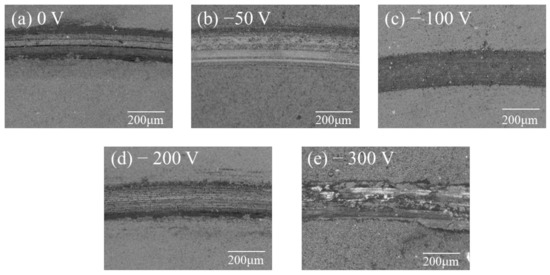
Figure 11.
Morphologies of the wear track of the AlCrSiN coatings deposited at different pulse bias voltages. (a) 0 V; (b) −50 V; (c) −100 V; (d) −200 V; (e) −300 V.
3.5. Electrochemical Properties
In the study of corrosion protection in 3.5 wt.% NaCl solutions, AlCrSiN coatings deposited at pulse biases of −100 V and −300 V were specifically investigated, as shown in Figure 12 and Figure 13. The OCP of all samples gradually rose with the immersion time and eventually reached steady states. The OCP values for uncoated 304 steel and AlCrSiN coatings prepared at −100 V and −300 V pulse biases were −166 mV, −125 mV, and −134 mV, respectively. Notably, the coating prepared at −100 V pulse bias exhibited the strongest corrosion resistance and the least corrosion tendency. This superior performance can be attributed to the lower number of defects, such as microcracks and pores, present in the coating. Furthermore, the corrosive medium first entered the coating surface, then the micro-cracks in the coating, and finally passed through the denser film layer before reaching the joint between the coating and the substrate. This process caused lattice distortion, leading to local cracking and bulging of the coating [33]. The EIS results further supported these findings. The Z0.01Hz, which is an indicator of electrode corrosion resistance [34], was 1.262 × 10⁶ Ω·cm2, 5.228 × 10⁶ Ω·cm2, and 4.624 × 10⁶ Ω·cm2 for uncoated 304 steel and AlCrSiN coatings at −100 V and −300 V, respectively. The coating prepared at −100 V bias voltage exhibited the highest impedance value, indicating better corrosion resistance. The presence of defects, such as microcracks, in the coating can serve as diffusion channels for corrosive ions (such as Cl−). The coating prepared at the bias voltage of −300 V has more defects than the coating prepared at the bias voltage of −100 V, as evidenced by the cross-sectional morphologies in Figure 4. Consequently, the impedance of the former coating is slightly smaller. Regardless of the number of defects, all coatings demonstrate a barrier effect that hinders the diffusion of corrosive ions, resulting in improved corrosion resistance. This effect effectively suppresses the corrosion process of the matrix metal by increasing the charge transfer resistance (about 3~4 times larger than that of the uncoated sample).
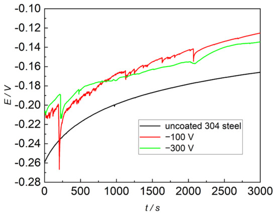
Figure 12.
The OCP of uncoated 304 steel and those of AlCrSiN coatings prepared at the bias voltage of −100 V and −300 V with immersion time in 3.5 wt.%NaCl solutions.
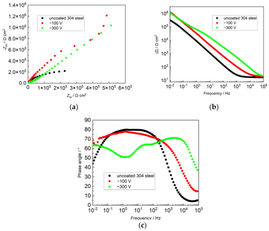
Figure 13.
The EIS of uncoated 304 steel and those with AlCrSiN coatings prepared at the bias voltage of −100 V and −300 V with immersion time in 3.5 wt.% NaCl solutions. (a) Nyquist plots; (b) Bode-modulus plots; (c) Bode-phase angle plots.
4. Conclusions
- (1)
- With the increase pulsed bias, the quantity and size of microparticles on the resulting AlCrSiN coatings first decreased and then increased, and reaching the minimum value as the bias voltage was −100 V.
- (2)
- With the increase in pulsed bias, the hardness, critical load, and wear resistance of the AlCrSiN coatings first increased and then decreased, and reached the maximum values as the bias voltage was −100 V. In this case, the coating hardness and critical load were 2668 HV and 72.7 N, respectively.
- (3)
- With the increase in the pulsed bias, the friction coefficient and wear rate of the AlCrSiN coatings first decreased and then increased. As the bias voltage was −100 V, the resulted coating presented the best tribological performance. The average friction coefficient and wear rate were 0.35 and 1.02 × 10⁻³ μm3/N·μm, respectively.
- (4)
- The AlCrSiN coatings significantly enhanced the corrosion resistance of 304 stainless steel, indicating that the AlCrSiN coating is a promising protective barrier in environments containing aggressive chloride ions.
Author Contributions
Conceptualization, all the authors; methodology, R.Z. and Y.L.; validation, C.W., Q.F. and F.C.; formal analysis, R.Z.; investigation, R.Z. and Y.L.; resources, T.W.; data curation, R.Z.; writing—original draft preparation, C.W.; writing—review and editing, Y.L.; supervision, T.W.; project administration, T.W.; funding acquisition, T.W. All authors have read and agreed to the published version of the manuscript.
Funding
This research was funded by Major Project of Tianjin Multi-investment Fund (22JCZDJC00670) and Scientific Research Project of Tianjin Education Commission (2021ZD005, 2022ZD020, 2022ZD033).
Informed Consent Statement
Informed consent was obtained from all subjects involved in the study.
Data Availability Statement
All raw data supporting the conclusion of this paper are provided by the authors.
Conflicts of Interest
The authors declare no conflict of interest.
References
- Jäger, N.; Meindlhumer, M.; Zitek, M.; Spor, S.; Hruby, H.; Nahif, F.; Julin, J.; Rosenthal, M.; Keckes, J.; Mitterer, C.; et al. Impact of Si on the high-temperature oxidation of AlCr(Si)N coatings. J. Mater. Sci. Technol. 2022, 100, 91–100. [Google Scholar] [CrossRef]
- Liang, J.; Almandoz, E.; Ortiz-Membrado, L.; Rodríguez, R.; de Ara, J.F.; Fuentes, G.G.; Jiménez-Piqué, E. Mechanical Performance of AlCrSiN and AlTiSiN Coatings on Inconel and Steel Substrates after Thermal Treatments. Materials 2022, 15, 8605. [Google Scholar] [CrossRef] [PubMed]
- Wang, T.G.; Jeong, D.; Liu, Y.M.; Wang, Q.M.; Iyengar, S.; Melin, S.; Kim, K.H. Study on nanocrystalline Cr2O3 films deposited by arc ion plating: II. Mechanical and tribological properties. Surf. Coat. Technol. 2012, 206, 2638–2644. [Google Scholar] [CrossRef]
- Zubizarreta, C.; Hernández, O.; Fernández-Martínez, I.; Ciarsolo, I.; Díez-Sierra, J.; Carreras, L.; Barriga, J. The effect of Bias configuration on the properties of AlCrN based thick coatings deposited by Cathodic Arc Evaporation. Appl. Surf. Sci. 2023, 610, 155543. [Google Scholar] [CrossRef]
- Zhang, S.H.; Wang, L.; Wang, Q.M.; Li, M.X. A superhard CrAlSiN superlattice coating deposited by multi-arc ion plating: I. Microstructure and mechanical properties. Surf. Coat. Technol. 2013, 214, 160–167. [Google Scholar] [CrossRef]
- Li, J.L.; Tan, C.B.; Luo, X.Y.; Xie, Z.J.; Zhong, X.L.; Wang, J.B.; Song, H.J. Preparation and toughness optimization of (AlCrSiN/TiN)20/Ti multilayer multiscale bionic tool coatings. Appl. Surf. Sci. 2023, 634, 157585. [Google Scholar] [CrossRef]
- Li, B.S.; Wang, T.G.; Ding, J.C.; Cai, Y.J.; Shi, J.; Zhang, X.T. Influence of N2/Ar flow ratio on microstructure and properties of the AlCrSiN coatings deposited by high-power impulse magnetron sputtering. Coatings 2017, 8, 3. [Google Scholar] [CrossRef]
- Gao, Y.; Cai, F.; Lu, X.; Xu, W.; Zhang, C.; Zhang, J.Z.; Qu, X.H. Design of cycle structure on microstructure, mechanical properties and tribology behavior of AlCrN/AlCrSiN coatings. Ceram. Int. 2022, 48, 12255–12270. [Google Scholar] [CrossRef]
- Li, M.; Yu, Y.J.; Zou, C.W.; Tian, C.X.; Wang, Z.S.; Xiang, Y.X. Wear and Corrosion Resistance of CrYN Coating in Artificial Seawater. Metals 2023, 13, 183. [Google Scholar] [CrossRef]
- Fan, Q.X.; Zhang, S.; Ma, D.Z.; Wu, Z.H.; Cao, F.T.; Liu, Y.M.; Wang, T.G. Bias voltage optimization and cutting performance of AlCrN coatings deposited by a hybrid technology. Vacuum 2022, 204, 111348. [Google Scholar] [CrossRef]
- Cai, F.; Gao, Y.; Fang, W.; Mao, T.J.; Zhang, S.H.; Wang, Q.M. Improved adhesion and cutting performance of AlTiSiN coatings by tuning substrate bias voltage combined with Ar ion cleaning pre-treatment. Ceram. Int. 2018, 44, 18894–18902. [Google Scholar] [CrossRef]
- Tang, J.F.; Lin, C.Y.; Yang, F.C.; Chang, C.L. Influence of nitrogen content and bias voltage on residual stress and the tribological and mechanical properties of CrAlN films. Coatings 2020, 10, 546. [Google Scholar] [CrossRef]
- Salamania, J.; Johnson, L.J.S.; Schramm, I.C.; Calamba, K.M.; Boyd, R.; Bakhit, B.; Odén, M. Influence of pulsed-substrate bias duty cycle on the microstructure and defects of cathodic arc-deposited Ti1-xAlxN coatings. Surf. Coat. Technol. 2021, 419, 127295. [Google Scholar] [CrossRef]
- Kang, M.S.; Wang, T.G.; Shin, J.H.; Nowak, R.; Kim, K.H. Synthesis and properties of Cr–Al–Si–N films deposited by hybrid coating system with high power impulse magnetron sputtering (HIPIMS) and DC pulse sputtering. Trans. Nonferrous Met. Soc. China 2012, 22, s729–s734. [Google Scholar] [CrossRef]
- Liang, J.; Serra, M.; Gordon, S.; de Ara, J.F.; Almandoz, E.; Llanes, L.; Jimenez-Piqué, E. Comparative Study of Mechanical Performance of AlCrSiN Coating Deposited on WC-Co and cBN Hard Substrates. Ceram. Int. 2023, 6, 1238–1250. [Google Scholar] [CrossRef]
- Petkov, N.; Bakalova, T.; Bahchedzhiev, H.; Kejzlar, P.; Rysanek, P.; Kormunda, M.; Capkova, P. Influence of the Addition of the Elements Ti and Cr on the Structure, and Mechanical and Tribological Properties of AlSiN Coatings. J. Nano Res. 2022, 73, 175–196. [Google Scholar] [CrossRef]
- Wang, T.G.; Jeong, D.; Kim, S.H.; Wang, Q.; Shin, D.W.; Melin, S.; Kim, K.H. Study on nanocrystalline Cr2O3 films deposited by arc ion plating: I. composition, morphology, and microstructure analysis. Surf. Coat. Technol. 2012, 206, 2629–2637. [Google Scholar] [CrossRef]
- Chen, Y.; Xu, Y.X.; Zhang, H.Q.; Wang, Q.M.; Wei, T.F.; Zhang, F.G.; Kim, K.H. Improving high-temperature wear resistance of arc-evaporated AlCrN coatings by Mo alloying. Surf. Coat. Technol. 2023, 456, 129253. [Google Scholar] [CrossRef]
- Jao, J.Y.; Han, S.; Chang, L.S.; Chang, C.L.; Liu, Y.C.; Shih, H.C. Bias voltage effect on the structure and property of chromium copper-diamond-like carbon multilayer films fabricated by cathodic arc plasma. Appl. Surf. Sci. 2010, 256, 7490–7495. [Google Scholar] [CrossRef]
- Qiu, Y.X.; Zhang, S.; Lee, J.W.; Li, B.; Wang, Y.X.; Zhao, D.L.; Sun, D. Towards hard yet self-lubricious CrAlSiN coatings. J. Alloys Compd. 2015, 618, 132–138. [Google Scholar] [CrossRef]
- Pribytkov, G.; Korzhova, V.; Korosteleva, E.; Krinitcyn, M. Effect of Silicon on the Surface Modification of Al-Cr Powder Cathodes Subjected to Vacuum Arc Treatment. Coatings 2022, 12, 958. [Google Scholar] [CrossRef]
- Zou, Z.M.; Dai, S.X.; Wang, R.D.; Li, Y.H.; Li, P.; Ge, F.F. Improvement of the high-temperature steam oxidation resistance of Zirlo tubes by multilayer Cr/CrAlSiN coatings. Surf. Coat. Technol. 2023, 466, 129616. [Google Scholar] [CrossRef]
- Luo, Y.; Dong, Y.Y.; Xiao, C.; Wang, X.T.; Peng, H. Impact Abrasive Wear Property of CrAlN/TiSiN Multilayer Coating at Elevated Temperatures. Materials 2022, 15, 2214. [Google Scholar] [CrossRef]
- Ahlgren, M.; Blomqvist, H. Influence of bias variation on residual stress and texture in TiAlN PVD coatings. Surf. Coat. Technol. 2005, 200, 157–160. [Google Scholar] [CrossRef]
- Cai, F.; Zhang, S.H.; Li, J.L.; Chen, Z.; Li, M.X.; Wang, L. Effect of nitrogen partial pressure on Al–Ti–N films deposited by arc ion plating. Appl. Surf. Sci. 2011, 258, 1819–1825. [Google Scholar] [CrossRef]
- Gong, H.X.; Huang, J.; Wang, J.J.; Zhao, P.B.; Liang, C.Y.; Guo, W.; Cao, R.Q.; Bai, D.Q. Research on the printing mechanism of electrohydrodynamic satellite-free droplets in pulsed voltage. J. Manuf. Process. 2023, 101, 300–310. [Google Scholar] [CrossRef]
- Cai, F.; Chen, M.H.; Li, M.X.; Zhang, S.H. Influence of negative bias voltage on microstructure and property of Al–Ti–N films deposited by multi-arc ion plating. Ceram. Int. 2017, 43, 3774–3783. [Google Scholar] [CrossRef]
- Polcar, T.; Cavaleiro, A. High-temperature tribological properties of CrAlN, CrAlSiN and AlCrSiN coatings. Surf. Coat. Technol. 2011, 206, 1244–1251. [Google Scholar] [CrossRef]
- Hsu, C.H.; Lin, C.Y.; Chen, J.X. Wear and Corrosion Performance of Ti-6Al-4V Alloy Arc-Coated TiN/CrN Nano-Multilayer Film. Metals 2023, 13, 907. [Google Scholar] [CrossRef]
- Wang, T.G.; Dong, Y.; Gebrekidan, B.A.; Liu, Y.M.; Fan, Q.X.; Kim, K.H. Microstructure and properties of the Cr–Si–N coatings deposited by combining high-power impulse magnetron sputtering (HiPIMS) and pulsed DC magnetron sputtering. Acta Met. Sin. 2017, 30, 688–696. [Google Scholar] [CrossRef]
- Sidashov, A.V.; Boiko, M.V.; Kozakov, A.T.; Manturov, D.S. Properties of CrAlSiN Coatings: Spectroscopic Research. Russ. Eng. Res. 2022, 42, 477–481. [Google Scholar] [CrossRef]
- Wang, T.G.; Zhao, S.S.; Hua, W.G.; Gong, J.; Sun, C. Design of a separation device used in detonation gun spraying system and its effects on the performance of WC-Co coatings. Surf. Coat. Technol. 2009, 203, 1637–1644. [Google Scholar] [CrossRef]
- Ghaziof, S.; Kilmartin, P.A.; Gao, W. Electrochemical studies of sol-enhanced Zn–Ni–Al2O3 composite and Zn–Ni alloy coatings. J. Electroanal. Chem. 2015, 755, 63–70. [Google Scholar] [CrossRef]
- Moshtaghi, M.; Safyari, M.; Mori, G. Hydrogen absorption rate and hydrogen diffusion in a ferritic steel coated with a micro-or nanostructured ZnNi coating. Electrochem. Commun. 2022, 134, 107169. [Google Scholar] [CrossRef]


Disclaimer/Publisher’s Note: The statements, opinions and data contained in all publications are solely those of the individual author(s) and contributor(s) and not of MDPI and/or the editor(s). MDPI and/or the editor(s) disclaim responsibility for any injury to people or property resulting from any ideas, methods, instructions or products referred to in the content. |
© 2023 by the authors. Licensee MDPI, Basel, Switzerland. This article is an open access article distributed under the terms and conditions of the Creative Commons Attribution (CC BY) license (https://creativecommons.org/licenses/by/4.0/).