Article

The Role of the Graphene Oxide (GO) and PEO Treated-Zinc Oxide (ZnO/PEO) Intermediate Electrode Buffer Layer in Vacuum-Free Quantum Dots Solar Cell

1
Research and Development Center, Korea Carbon Industry Promotion Agency, 110-11 Banryong-Ro, Jeonju 54853, Republic of Korea
2
Department of Physics, Kyungpook National University, 80 Daehak-Ro, Daegu 41566, Republic of Korea
3
School of Chemical Engineering, Yeungnam University, 280 Daehak-Ro, Gyeongsan 38541, Republic of Korea
*
Authors to whom correspondence should be addressed.
Metals 2022, 12(12), 2096; https://doi.org/10.3390/met12122096
Submission received: 17 October 2022 / Revised: 25 November 2022 / Accepted: 28 November 2022 / Published: 6 December 2022

Abstract

:
The vacuum-free quantum dots solar cell (VFQDSC) was fabricated without using any vacuum process. The spherical iron pyrite (FeS2) nanoparticles (SNPs) and ZnO nanoparticles (NPs) were synthesized and characterized. In the device structure, FeS2 SNPs were used as an acceptor material (n-type), and the low band gap polymer of poly[4,8-bis(2-ethylhexyloxyl)benzo[1,2-b:4,5-b′]-dithiophene-2,6-diyl-alt-ethylhexyl-3-fluorothieno[3,4-b]thiophene-2-carboxylate-4,6-diyl] (PBT7) was used as a donor material (p-type). In this study, we first applied the graphene oxide (GO) as the hole transport buffer layer (HTBL) and zinc oxide (ZnO) as an electron transport buffer layer (ETBL), which were considered to improve the charge transportation efficiency of the device’s system. The device with the structure of the Glass/ITO/HTBL/FeS2 SNPs, PBT7/ ETBL/E-GaIn were fabricated with a maximum power conversion efficiency (PCE) of 3.6%.

1. Introduction

In order to compensate for the continuously depleting stock of fossil fuels such as coal, oil, and natural gas, the exploitation of the renewable energy such as biomass, wind power, hydro power, and especially solar energy via solar cells technology is one of most appealing solutions. There are many types of high-power conversion efficiency solar cells in the 10–30% range of efficiency such as DSSCs, silicon, perovskite, CIGS, and CZTS [1,2,3,4]. However, these technologies still have some disadvantages such as high costs, toxicity, and a lack of materials, etc. Quantum dots (Qdots) are solution-based synthesized nanoparticles for most semiconductor compounds. Qdots are synthesized as colloids in organic solvents with the added benefits of their shape, ligand, size- tunable optical and electrical properties [5]. The diameter of the Qdots are smaller to the Bohr exciton, which allows the band gap of the Qdots to be tuned by controlling the size of the nanocrystal. Quantum dots (Qdots) and conjugate polymer-based hybrid solar cells have been investigated by many research groups worldwide as being viable as they have a low cost, simple solution process, and easy fabrication [6,7]. Besides a lot of the advantageous properties, the quantum dots solar cells now are facing serious challenges in the developing highly efficient Qdot-based devices due to bulk recombination losses, low light absorption, active layer morphology, low carrier transportation, low Ohmic contact between the active layer and electrodes, and the short exciton diffusion length (10~15 nanometers) causing less efficient charge separation and transport to the respective electrodes as well as the limitation in the device fabrication [8,9]. Among these reasons, low Ohmic contact between the photoactive layer and the back and front contact is the main reason that made the device had a low efficiency. Moreover, this problem could be overcome by optimizing the surface morphology and improving the transportation of the holes and electrons using the hole transport (HT) and electron transport buffer layer (ETBL).
Poly(3,4-ethylenedioxythiophene)-poly(styrenesulfonate)(PEDOT: PSS) has been selected as an HTBL for many types of solar cells structure because of its good ability, good visible transparency, and appropriate band gap energy. However, PEDOT:PSS is sensitive to oxygen which can introduce the water into the photoactive layer of the device. It has high acidity and hygroscopic properties, thus degrading the device’s performance [10,11,12,13]. Recently, graphene oxide (GO) has been used for many applications in electronic devices as interlayer materials [14,15,16]. GO has been prepared by very simple methods using a low-cost solution-based process [17]. Especially, GO has been used as a buffer layer in solar cells, and the studies have shown that by using GO, the device’s efficiency has increased [14,18,19]. The studies have shown that by using the GO buffer layer, the device showed improvement in the current density and open circuit voltage due to the reduced interference between the sunlight and the decomposition of the CZTSSe. This reduction lead to a decrease in the defects state and an increase in the device’s efficiency.
For ETBL, zinc oxide (ZnO) is a promising electron transport material with a wide band gap (~3.3 eV), it is abundant in the earth, it is simple to synthesize, it has a non-toxic nature, and it can be easily tuned by changing its structures and morphology. In organic/inorganic bulk hetero-junction solar cells, ZnO has been used as a charge carrier mobility to overcome the charge transport limitation [20,21,22]. The effects of ZnO NP surface modification using poly (ethylene oxide)(PEO) on the performance of hybrid solar cells based on poly[2-methoxy-5-(2′-ethylhexyloxy)-1,4-phenylene vinylene] (MEH-PPV) have been studied. The device had less resistance, less charge recombination, and enhanced electrical coupling between the ZnO NPs and the polymer, leading to an increase in the power conversion efficiency.
Iron pyrite (FeS2) Qdots have been investigated as a promising material with high light absorption, a simple synthesis, and abundant elements [23,24]. The hybrid solar cell based on FeS2 nanoparticles and poly(3-hexylthiophene) (P3HT) have been investigated and fabricated with the highest power conversion efficiency of about 3.0%. There are many methods that can be used to improve the power conversion efficiency of the solar cells, including controlling the surface morphology by a thermal treatment, plasmonic incorporation, or by adding a buffer layer between the electrode and the device’s active layer, etc.
In this study, we have fabricated a vacuum-free quantum dots solar cell with the structure of ITO/PEDOT:PSS (or GO)/( FeS2 + PBT7)/ZnO (PEO)/ E-GaIn. The materials such as GO, FeS2 Qdots, and ZnO were synthesized in a laboratory and characterized. FeS2 Qdots were used as the n-type material, and PBT7 was used as p-type material. The GO and PEDOT:PSS were used as the HTBL, and ZnO was used as ETBL of the fabricated devices. E-GaIn (purchased form Sigma Aldrich) used as the cathode was deposited on the top of the ZnO/PEO film by a doctor-blading process. The effects of GO and ZnO on the device’s performance were also investigated by measuring the surface morphology and the device’s efficiency. The device performance was enhanced by optimizing the active layer’s surface morphology and increasing the charge carriers transport from the active layer to the back and front contact.

2. Materials and Methods

2.1. Synthesis of Graphene Oxide

The graphene oxide flakes were synthesized using the modified Hummers method [25]. In detail, graphite (2 g) (Mesh100, Sigma-Aldrich, St. Louis, MO, USA) was mixed into (100 mL) of concentrated Sulfuric acid (H2SO4) (Mesh100, Sigma-Aldrich, St. Louis, MO, USA) under a stirring condition at room temperature, then, 12 g of Potassium Permanganate (KMnO4) (Mesh100, Sigma-Aldrich, St. Louis, MO, USA) was slowly added to the mixture, and it was stirred for 2 h. When the color of the mixture turned to dark green color, 250 mL of deionized water (DI) was slowly added, and the solution was stirred for 10 min at room temperature. An additional 200 mL of DI water was added, and it was stirred for 24 h at room temperature. The product was sonicated for 2 h, filtered, and dried at 100 °C for 15 h, and then, dried at 350 °C for 24 h. Finally, the GO flakes were obtained

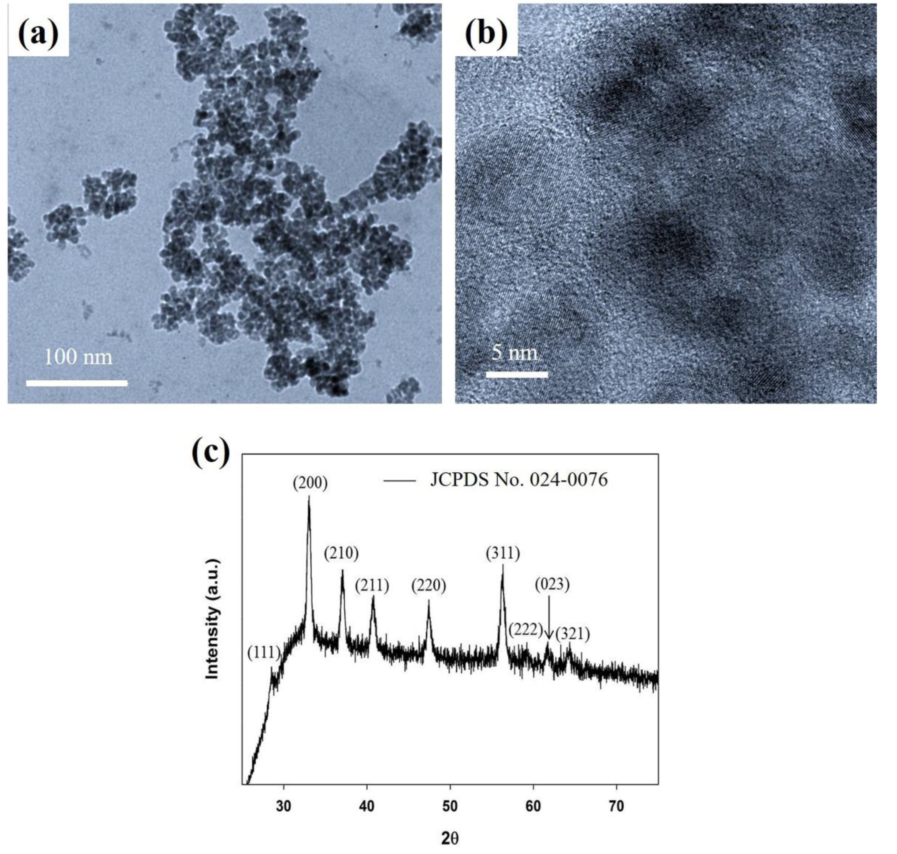
2.2. Synthesis of Iron Pyrite (FeS2) Spherical Nanoparticles (SNPs)

The FeS2 spherical nanoparticles were prepared by using a modified hot injection method [26]. Initially, 1 mmol of FeCl2.4H2O (Mesh100, Sigma-Aldrich, St. Louis, MO, USA) and 20 g octadecylamine (ODA) (Mesh100, Sigma-Aldrich, St. Louis, MO, USA) were added to a three-neck flask and heated to 120 °C for 1 h to form the ODA-capped Fe solution. In parallel, 6 mmol of sulfur in 10 mL diphenyl ether was stirred in a beaker at 70 °C for 1 h to form the sulfur solution.
The sulfur solution was quickly injected into the Fe solution in the flask when the temperature reached 200 °C. The nanocrystals were grown at 200 °C for 3 h, and then, they were cooled down to 100 °C. When the temperature was below 100 °C, the chloroform (18 mL) was added to prevent the ODA from solidifying, the temperature was then cooled down to room temperature. The final products were then diluted to chloroform and centrifuged several times at 4000 rounds per minutes (rpm) for 5 min.

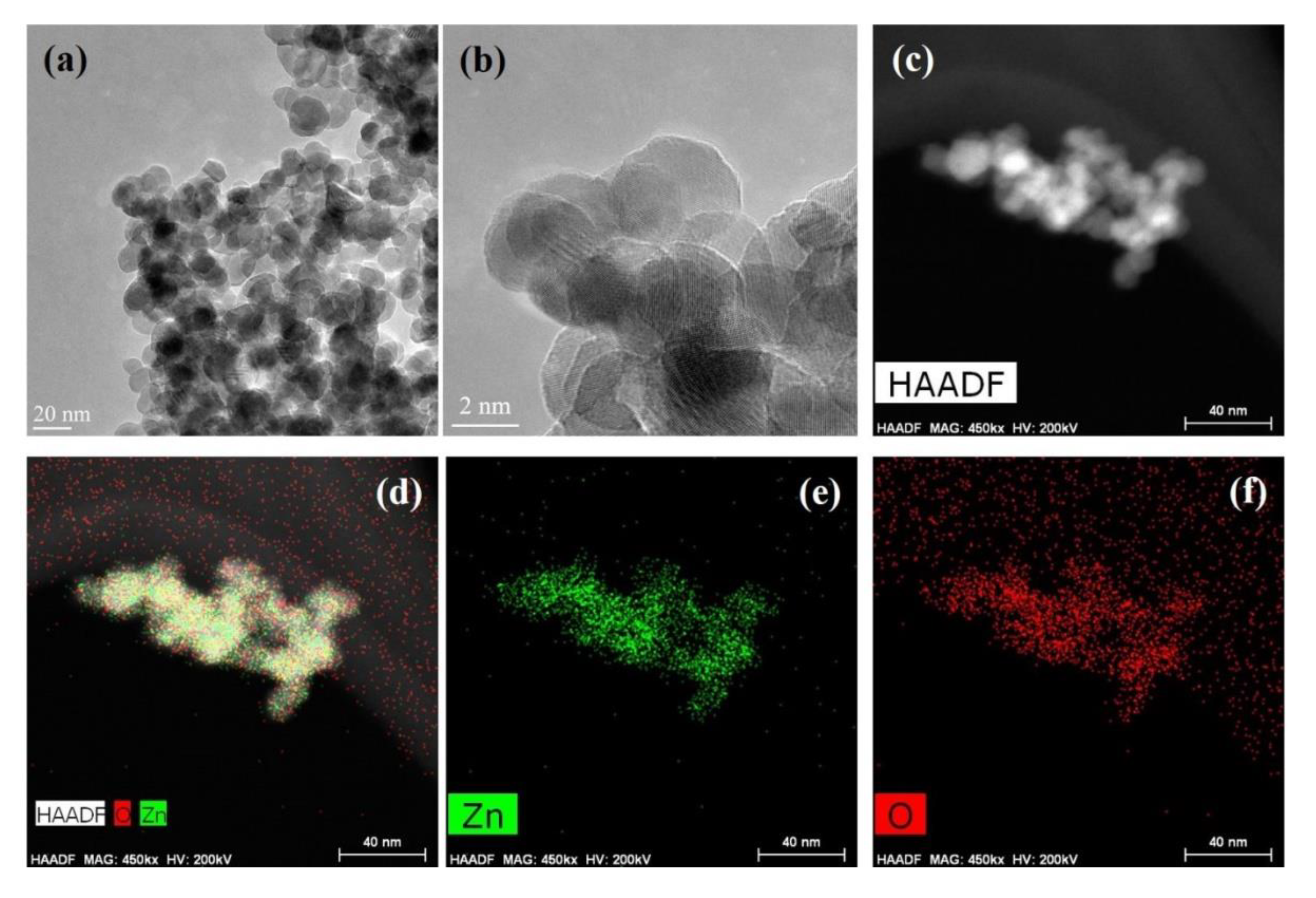
2.3. Synthesis of Zinc Oxide (ZnO) Spherical Nanoparticles

In this work, zinc oxide spherical nanoparticles were synthesized in the laboratory with an average size of ~3–8 nm. In detail, the ZnO nanoparticles were synthesized using the direct precipitation method. In detail, the aqueous solution (0.2 M) of zinc nitrate (Zn(NO3 ) 2 .6H2O) (Mesh100, Sigma-Aldrich, St. Louis, MO, USA) and the solution (0.4 M) of potassium hydroxide (KOH) (Mesh100, Sigma-Aldrich, St. Louis, MO, USA) which was prepared with deionized water was slowly added into the aqueous solution (0.2 M) of zinc nitrate (Zn(NO3 ) 2 .6H2 O) at room temperature under a vigorous stirring condition. The white product was centrifuged at 6000 rpm for 30 min and washed several times with distilled water. Finally, the ZnO nanoparticles were obtained. The morphological and composition properties of the ZnO NPs were analyzed using the TEM and TEM mapping techniques. The ZnO film (~30 nm of thick) was spin coated on the top of the active layer with a spin speed of 4000 rpm for 40 s, and then, it was dried at 120 °C for 10 min to form the electron transport layer.

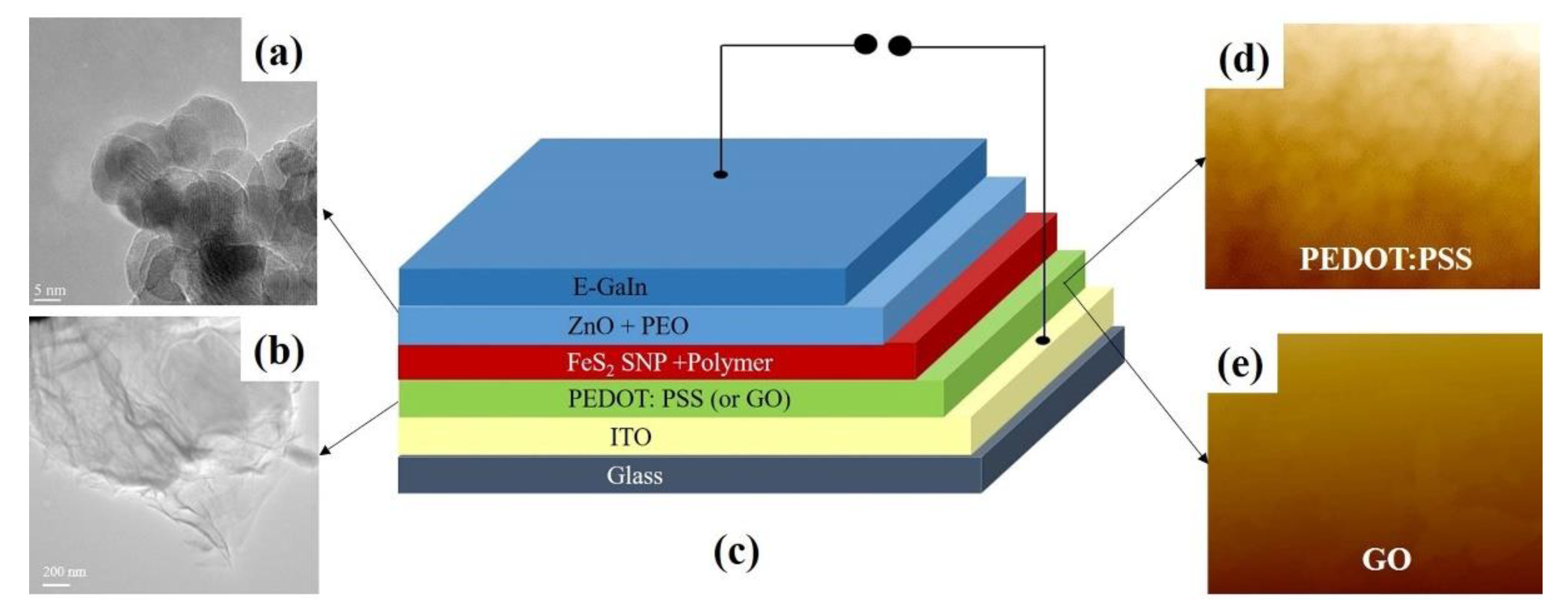
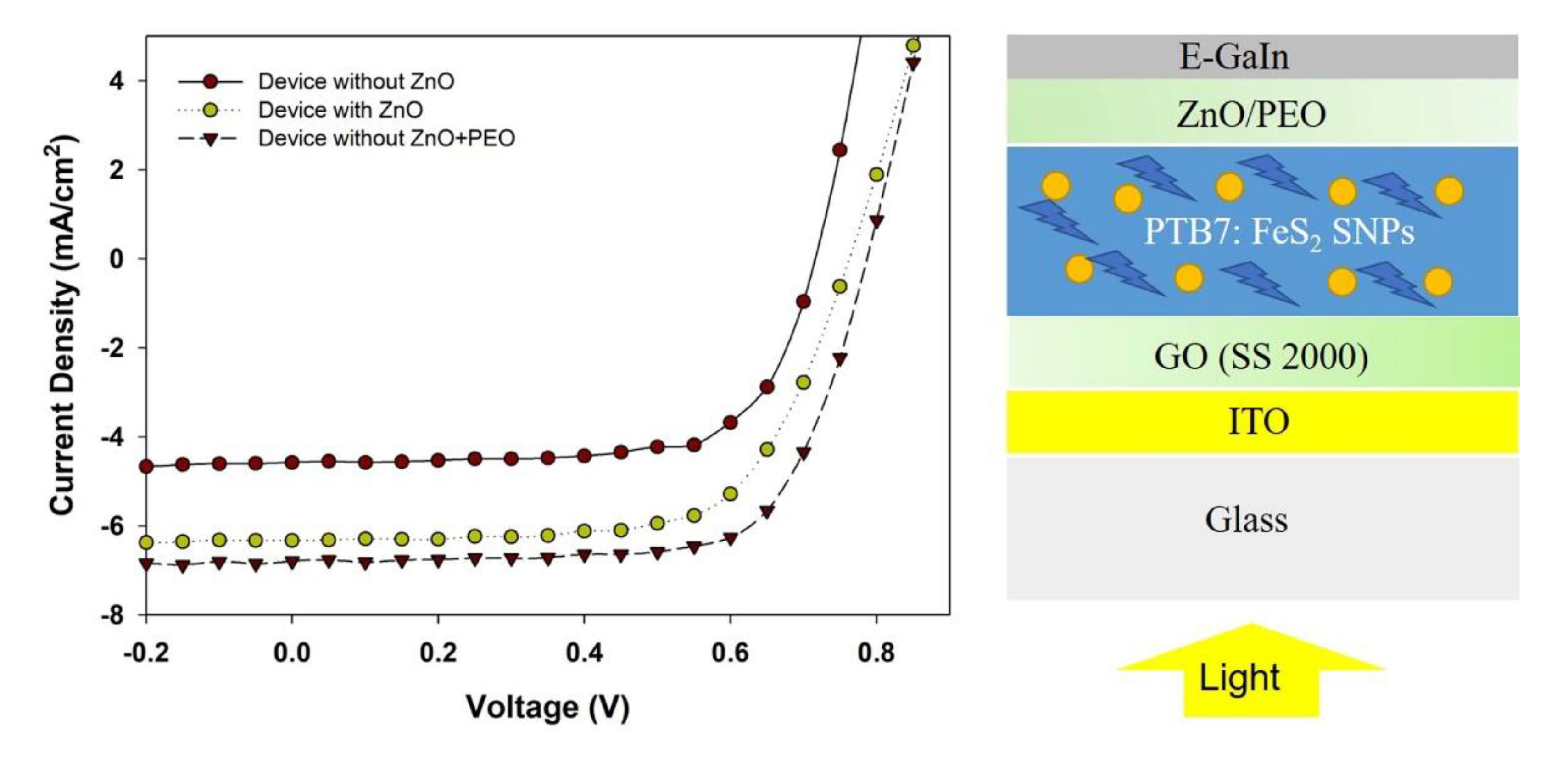
2.4. Device Fabrication

The VFQDSCs were prepared to produce the following structure of ITO-coated glass/hole transport layer/(FeS2 + PBT7)/electron transport layer/E-GaIn. Firstly, an HTL of PEDOT: PSS was deposited onto cleaned indium tin oxide (ITO)-coated glass substrates, and then, it was dried at 100 °C for 30 min. An HTL of graphene oxide was deposited at different of spin speeds (SS) of 1000, 2000, and 3000 rpm onto cleaned indium tin oxide (ITO)-coated glass substrates, and they, they were dried at 100 °C for 30 min. The active layer solution of FeS2 + PBT7 was deposited onto the ITO/PEDOT:PSS (GO) at 1500 rpm of the spin coater’s speed for 60 s, then, it was dried at 120 °C for 20 min to form the active layers. Then, a thin layer of ZnO was deposited onto the active layer to form the ETL. Finally, E-GaIn (device’s cathode) was deposited to complete the device structure of the Glass/ ITO//PEDOT:PSS (or GO)/(FeS2 + PBT7)/ZnO/E-GaIn, as shown in Figure 1c.

2.5. Characterization

The morphological properties of the FeS2, GO, and ZnO nanoparticles were confirmed using transmission electron microscopy (TEM) and high-resolution TEM (HR-TEM) (Field Emission Transmission Electron Microscope; Model: FEI company). The structural properties of these nanomaterials were measured using X-ray Diffraction (XRD) (Model: PANalytical X’ pert PRO). The surface roughness (RMS) was measured by using the atomic force microscopy (AFM) technique (Model: Park NX10). The composition of the ZnO nanoparticles was analyzed using the TEM mapping technique.
The device’s parameters such as the (FF) Fill factor (%), (Jsc) short circuit current density (mA/cm2), (Voc) open circuit voltage (V), and (PCE) power conversion efficiency (%) were characterized using a solar simulator (Keithley 69911) (Beaverton, OR, USA) under AM 1.5 illumination at 100 mW/cm2.

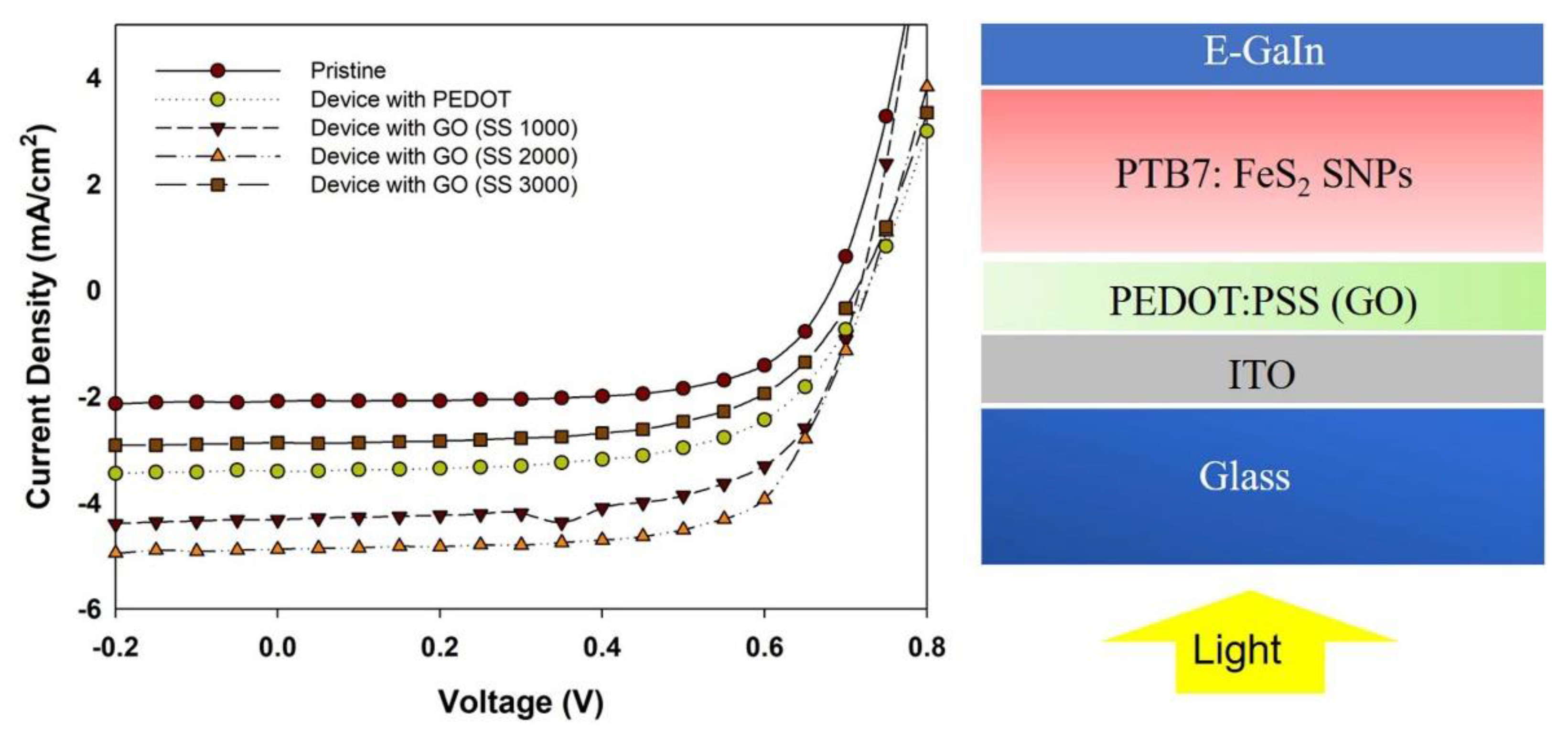
3. Results and Discussions

Figure 1a shows the TEM image of the ZnO spherical nanoparticles, which have a size in the range of 3~8 nm, and Figure 1b shows the TEM image of the synthesized GO flake shape. In this work, GO was used as a hole transport buffer layer, and ZnO was used as an electron transport buffer layer. The VFQDSCs with an active area of 0.44 mm2 were prepared in the structure of glass/indium tin oxide (ITO)/HTBL/FeS2 + PBT7/ETBL/E-GaIn. The schematic of the device’s structure is shown in Figure 1c. Two HTBL of GO and PEDOT:PSS were used for a comparison. Both of GO and PEDOT:PSS were deposited on the glass/ITO substrate using the solution method. In this study, the GO was dispersed in deionized (DI) water at 0.2 mg/mL, and the GO solution was coated onto the glass/ITO using a spin-coating method. The topography of the GO and PEDOT:PSS films on the ITO was measured using atomic force microscopy (AFM) (Figure 1d,e). The surface roughness of the GO film is about ~1.55 nm, which is smaller than that of PEDOT:PSS film (about ~3.5 nm). The smoother surface of the GO film can provide a good contact with the photoactive layer, leading to improving of hole collection efficiency from the active layer to the electrode of the ITO.
The photoactive layer of the device includes FeS2 spherical nanoparticles as an n-type material and a low band gap polymer as a p-type material. As the size of the SNPs is in the range of 3 to 10 nm, the TEM technique was used to investigate the exact microstructure of FeS2, as shown in Figure 2. The TEM and high resolution (HR-TEM) images of SNPs are shown in Figure 2a and Figure 2b, respectively. The fringe distance of ~0.53 nm in the lattice fringe of FeS2 matches well to the distance between the planes of (200) and (010) planes in the cubic structure, which reveals the successful synthesis of high quality and very highly crystalline of cubic FeS2 SNPs [27,28,29]. The structure of the FeS2 SNPs was investigated using the X-ray diffraction (XRD) technique, which presented that the FeS2 SNPs had a cubic structure with crystal planes of (111), (220), and (311), corresponding to the peaks of 25.2, 41.9, and 49.7° in our previous work, respectively [30]. The HR-TEM images and XRD crystal planes clearly confirm that the phase of the FeS2 SNPs was very highly crystalline with the cubic phase structure.
The topography and three-dimensional (3D) images of the surface roughness of the ITO/PEDOT: PSS (or GO)/FeS2 + PBT7 without PEDOT: PSS and GO are displayed in Figure 3a–f. With PEDOT: PSS, the (FeS2 + PBT7) film had a roughness of 6.66 nm, which was smaller than that without the PEDOT:PSS film (~8.43 nm), as shown in Figure 3a,b. The roughness of the FeS2 + PBT7 film with a different spin speed (SS) of the GO (SS 1000, SS 2000, and SS 3000) were also investigated, as shown in Figure 3c–f. With GO (SS 2000) (as Figure 3d), the (FeS2 + PBT7) film had the smallest roughness of 3.54 nm. The result depicts that by using PEDOT: PSS and GO as the hole transporting buffer layer, the surface roughness of the photoactive layers was improved.
The current density–voltage curves under AM 1.5 G illumination at 100 mW/cm2 of the planar VFQDSCs using PEDOT: PSS or GO as the HTBL are shown in Figure 4. The device’s parameters determined from these solar cells are also summarized in Table 1. The pristine device showed a PCE of 0.93% with Voc of 0.67 V, a Jsc of 2.09 mA/cm2, and a fill factor (FF) of 65.7%. The PEDOT: PSS-based device exhibited a PCE of 1.48% with a Voc of 0.67 V, a Jsc of 3.40 mA/cm2, and a fill factor (FF) of 60.1%. When the PEDOT: PSS was replaced by the GO (SS 2000), the PCE was increased to 2.3% with a Voc of 0.67 V, a Jsc of 5.48 mA/cm2, and a fill factor (FF) of 70.43%. The PEDOT: PSS film had an advantage that it was spin coated onto the ITO from the solution, and it had a smooth surface as well to align the work function of the polymer and ITO for a larger collection of holes [31,32,33]. However, the PEDOT: PSS film was deposited from a highly acidic (pH~1) aqueous suspension, leading it to have water into the photoactive layer of the device that affected to the device’s performance. Using GO as a hole transport buffer layer resulted in high conductivity and a high work function [34]. The high conductivity leads to the high charge carrier’s collection efficiency and a high short-circuit current density (Jsc). The high work function can lead to ohmic contact and improve the built-in potential and increase the open circuit voltage (Voc). Besides that, the ITO/GO surface roughness was also measured by AFM, as shown in Figure 3. The surface of the ITO/GO was smoother in comparison to that of ITO/PEDOT:PSS, leading to it improving the contact between the active layer and the ITO anode. The hole collection efficiency is increased, leading to and increase in the current density and the device’s efficiency.
There are many methods that can be to improve the device’s performance, including controlling the active layer’s surface morphology, increasing the absorption percentage, improving the charge transportation, etc. The increase in the electron collection efficiency is one of the best methods. In this device structure, ZnO was used as an electron transport buffer layer, which has two functions: ZnO was used as the electron transport material, and the ZnO thin layer was used to control the surface morphology of the photoactive layer, leading to an enhancement of the contact between the active layer and the negative electrode (E-GaIn). The HR-TEM and TEM mapping techniques were used to investigate the exact microstructure of ZnO, as shown in Figure 5. The TEM and high resolution (HR-TEM) images of SNPs are shown in Figure 5a,b, revealing the successful synthesis of high quality ZnO SNPs. Figure 5c–f further shows the elemental mapping of the nanostructures, confirming the good uniformity of the ZnO nanocrystal structure. The results confirm that the phase of the ZnO SNPs was very highly crystalline and of a high quality.
The effects of ZnO and ZnO/PEO as an electron acceptor on the performance of the MEH-PPV/ZnO hybrid solar cells were investigated [21]. They reported that the device using ZnO/PEO with a small amount of PEO showed a considerably reduced series resistance and it increased the shunt resistance of the device due to the passivated surface traps of the ZnO NPs. The device’s efficiency was increased due to improvement of the electron transport and restrained back charge carrier recombination.
In this work, the ZnO and ZnO/PEO were used as the electron transport buffer layer between the active layer and the electrode. The effects of ZnO and ZnO/PEO on the morphological and electrical properties of the device were investigated by taking measurements of surface’s roughness using atomic force microscopy (AFM) and the solar simulation technique, as shown in Figure 6 and Figure 7, respectively.
The effects of ZnO and ZnO/PEO on the surface roughness of the photoactive layer were studied, and they are shown in Figure 6. Without the ZnO layer, the roughness of the photoactive layer is about 3.54 nm. With ZnO and ZnO/PEO, the roughness values of the photoactive layer are 1.52 nm and 0.85 nm, respectively. The active layer with ZnO/PEO have the smoothest surface in comparison with the other cases. The device’s active layer had a smoother surface which allows for good contact between the active layer and the electrode.
Figure 7 shows the illuminated J–V curves of the devices without and with ZnO and ZnO/PEO as a buffer layer under 100 mW/cm2 of the AM 1.5 G condition, and the device’s parameters are listed in Table 2. The pristine device without ZnO shows an efficiency (PCE) of about ~2.30% (Jsc: 4.58 mA/cm2, Voc: 0.67 V, FF: 70.43%). The device’s performance was considerably enhanced when ZnO and ZnO/PEO were used as an electron transport buffer layer. The device with ZnO shows an efficiency of about ~3.14% (Jsc: 6.33 mA/cm2, Voc: 0.77 V, FF: 65.74%). With ZnO/PEO, the optimized device shows a PCE of about ~ 3.61% (Jsc: 6.70 mA/cm2, Voc: 0.77 V, FF: 70.04%). The results show that using ZnO and ZnO/PEO as an ET buffer layer leads to an improvement of the device’s performance due to increase in the current density from 4.58 to 6.70 mA/cm2.
The increase in the device’s current density might be explained by two reasons. Firstly, the improvement of the contact between the active layer and the cathode (E-GaIn) leads to an increase in the electron collection efficiency at the (FeS2 SNPs + PBT7)/cathode interface. Secondly the reduction of the series resistance (Rs) and the increase in the shunt resistance (Rsh) was observed in the device using ZnO and ZnO/PEO, as shown in Table 2. The device using ZnO/PEO shows a smaller Rs and higher Rsh values (Rs = 35 Ω cm2, Rsh = 2.1 kΩ cm2) compared to the ZnO device (Rs = 69 Ω cm2, Rsh = 1.52 kΩ cm2) and the pristine device (Rs = 85 Ω cm2, Rsh = 1.02 kΩ cm2). The decreased Rs of the device with ZnO and ZnO/PEO as the ETBL is responsible for charge carriers transport and electron collection efficiency, which explains the improvement of the short current density. The increased Rsh indicates that the recombination loss of charge carriers were reduced due to the current leakage pathways in the photoactive layer [35,36]. The smooth surface of the ZnO/PEO buffer layer sandwiched between the photoactive layer (FeS2 + PBT7) and the cathode (E-GaIn) provided good contact and enhanced electron collection efficiency to the cathode.
With the hybrid solar cells structure, the recorded power conversion efficiency of the PbS quantum dots solar cells is about ~4.9% [37]. Compared with the recorded efficiency (~4.9%), that of the vacuum-free Qdots hybrid solar cells in this study is smaller. However, for the FeS2 quantum dots hybrid solar cells structure [23,24], our device’ efficiency has the highest value of 3.6%. The stability and reproducibility of the device was investigated by fabricating the device under optimized conditions three times. The results show that the average values of the device’s parameters such as its efficiency is about ~3.75% (Jsc: 7.3 mA/cm2; Voc: 0.75 V; FF: 67.4). To improve the efficiency, the nanostructure, charge carrier transport, and sunlight absorption, etc., of the device should be optimized.

4. Conclusions

Zinc oxide and graphene oxide were successfully synthesized, characterized, and applied to vacuum-free quantum dots solar cells as the charge carriers buffer layer. When the thin layer of GO (SS 2000) was used as a hole transport layer, the device’s efficiency was increased due to an improvement of the ohmic contact between the active layer and the anode. The smooth surface of the ZnO/PEO layer sandwiched between the device’s active layer and the cathode provided a good ohmic contact, and it enhanced the electron collection efficiency of the cathode. In the optimized condition, the power conversion efficiency of the device using GO and ZnO/PEO as a hole and electron transport layer was increased, with maximum power conversion efficiency of ~3.61% (Jsc: 6.70 mA/cm2, Voc: 0.77 V, FF: 70.04%).

Author Contributions

Writing—original draft preparation, Conceptualization, Data interpretation, Writing—review and editing, N.T.N.T.; Data curation, Validation, Resource, S.B.K. and Y.J.; Visualization, Formal analysis, N.H.L.; Supervision, J.H.J.; Project administration, Funding acquisition, C.-D.K. All authors have read and agreed to the published version of the manuscript.

Funding

This work was supported by the Materials/Parts Technology Development Program (20007170, Development of carbon materials for fuel cell electrode of FCEV), the Technology Innovation Program (20006820, Development of automated system for electrochemical exfoliation of synthetic graphite production residue and multifunctional composites) funded by the Ministry of Trade, Industry and Energy (MOTIE, Korea). A portion of this work was supported by Basic Science Research Program through the National Research Foundation of Korea (NRF) funded by the Ministry of Education (grant number NRF-2022R1I1A1A01071414).

Institutional Review Board Statement

Not applicable.

Informed Consent Statement

Not applicable.

Data Availability Statement

Not applicable.

Conflicts of Interest

The authors declare that they have no known competing financial interest or personal relationships that could appear to influence the work reported in this paper.

References

  1. Shaikh, S.M.F.; Rahman, G.; Mane, R.S.; Joo, O.S. Bismuth oxide nanoplates-based efficient DSSCs: Influence of ZnO surface passivation layer. Electrochim. Acta 2013, 111, 593–600. [Google Scholar] [CrossRef]
  2. Blakers, A.; Zin, N.; McIntosh, K.R.; Fong, K. High-efficiency silicon solar cells. Energy Procedia 2013, 33, 1–10. [Google Scholar] [CrossRef] [Green Version]
  3. Fradi, K.; Bouich, A.; Slimi, B.; Chtourou, R. Towards improving the optoelectronics properties of MAPbI3(1−x)B3x/ZnO heterojunction by bromine doping. Optik 2022, 249, 168283. [Google Scholar] [CrossRef]
  4. Khalate, S.A.; Kate, R.S.; Deokate, R.J. A review on energy economics and the recent research and development in energy and the Cu2ZnSnS4 (CZTS) solar cells: A focus towards efficiency. Sol. Energy 2018, 169, 616–633. [Google Scholar]
  5. Steinmann, V.; Kronenberg, N.M.; Lenze, M.R.; Graf, S.M.; Hertel, D.; Meerholz, K.; Burckstummer, H.; Tulyakova, E.V.; Würthner, F. Simple, Highly Efficient Vacuum-Processed Bulk Heterojunction Solar Cells Based on Merocyanine Dyes. Adv. Energy Mater. 2011, 1, 888–893. [Google Scholar] [CrossRef]
  6. She, X.J.; Liu, J.; Zhang, J.Y.; Gao, X.; Wang, S.D. Spatial profile of charge storage in organic field-effect transistor nonvolatile memory using polymer electret. Appl. Phys. Lett. 2013, 103, 184. [Google Scholar] [CrossRef]
  7. Yang, B.; Xiao, Z.; Huang, J. Polymer aggregation correlated transition from Schottky-junction to bulk heterojunction organic solar cells. Appl. Phys. Lett. 2014, 104, 54. [Google Scholar] [CrossRef] [Green Version]
  8. Ma, W.; Yang, C.; Gong, X.; Lee, K.; Heeger, A.J. Thermally stable, efficient polymer solar cells with nanoscale control of the interpenetrating network morphology. Adv. Funct. Mater. 2005, 14, 1617–1622. [Google Scholar] [CrossRef]
  9. Ma, B.; Woo, C.H.; Miyamoto, Y.; Fréchet, J.M. Rapid room-temperature synthesis and characterization of nanocrystals of a prototypical zeolitic imidazolate framework. Chem. Mater. 2009, 21, 1410–1412. [Google Scholar]
  10. Chiang, C.H.; Wu, C.G. Bulk heterojunction perovskite–PCBM solar cells with high fill factor. Nat. Photonics 2016, 10, 196–200. [Google Scholar] [CrossRef]
  11. You, J.B.; Meng, L.; Song, T.B.; Guo, T.F.; Yang, Y.M.; Chang, W.H.; Hong, Z.R.; Chen, H.J.; Zhou, H.P.; Chen, Q.; et al. Improved air stability of perovskite solar cells via solution-processed metal oxide transport layers. Nat. Nanotechnol. 2016, 11, 75–81. [Google Scholar] [CrossRef] [PubMed]
  12. Ma, R.; Zeng, M.; Li, Y.; Liu, T.; Luo, Z.; Xu, Y.; Ping, L.; Nan, Z.; Jianfeng, L.; Yuan, L.; et al. Rational anode engineering enables progresses for different types of organic solar cells. Adv. Energy Mater. 2021, 11, 2100492. [Google Scholar] [CrossRef]
  13. Hou, Y.; Wang, Q.; Huang, C.; Yang, T.; Shi, S.; Yao, S.; Donglou, R.; Tao, L.; Guangye, Z.; Zou, B. Controlling the Treatment Time for Ideal Morphology towards Efficient Organic Solar Cells. Molecules 2022, 27, 5713. [Google Scholar] [CrossRef]
  14. Wu, Z.W.; Bai, S.; Xiang, J.; Yuan, Z.C.; Yang, Y.G.; Cui, W.; Gao, X.Y.; Liu, Z.; Jin, Y.Z.; Sun, B.Q. Efficient planar heterojunction perovskite solar cells employing graphene oxide as hole conductor. Nanoscale 2014, 6, 10505–10510. [Google Scholar] [CrossRef] [PubMed]
  15. Agresti, A.; Pescetelli, S.; Cina, L.; Konios, D.; Kakavelakis, G.; Kymakis, E.; Carlo, A.D. Efficiency and stability enhancement in perovskite solar cells by inserting lithium-neutralized graphene oxide as electron transporting layer. Adv. Funct. Mater. 2016, 26, 2686–2694. [Google Scholar] [CrossRef]
  16. Zhu, Y.W.; Murali, S.; Cai, W.W.; Li, X.S.; Suk, J.W.; Potts, J.R.; Ruoff, R.S. Graphene and graphene oxide: Synthesis, properties, and applications. Adv. Mater. 2010, 22, 3906–3924. [Google Scholar] [CrossRef]
  17. Eda, G.; Fanchini, G.; Chhowalla, M. Large-area ultrathin films of reduced graphene oxide as a transparent and flexible electronic material. Nat. Nanotechnol. 2008, 3, 270–274. [Google Scholar] [CrossRef]
  18. Jeong, W.L.; Park, S.H.; Jho, Y.D.; Joo, S.K.; Lee, D.S. The Role of the Graphene Oxide (GO) and Reduced Graphene Oxide (RGO) Intermediate Layer in CZTSSe Thin-Film Solar Cells. Materials 2022, 15, 3419. [Google Scholar] [CrossRef]
  19. Lee, D.Y.; Na, S.I.; Kim, S.S. Graphene oxide/PEDOT: PSS composite hole transport layer for efficient and stable planar heterojunction perovskite solar cells. Nanoscale 2016, 8, 1513–1522. [Google Scholar] [CrossRef]
  20. Oosterhout, S.D.; Wienk, M.M.; van Bavel, S.S.; Thiedmann, R.; Koster, L.J.A.; Gilot, J.; Loos, J.; Schmidt, V.; Janssen, R.A.J. The effect of three-dimensional morphology on the efficiency of hybrid polymer solar cells. Nat. Mater. 2009, 8, 818–824. [Google Scholar] [CrossRef]
  21. Shao, S.; Zheng, K.; Zidek, K.; Chabera, P.; Pullerits, T.; Zhang, F. Optimizing ZnO nanoparticle surface for bulk heterojunction hybrid solar cells. Sol. Energy Mater. Sol. Cells 2013, 118, 43–47. [Google Scholar] [CrossRef] [Green Version]
  22. Tian, Z.R.; Voigt, J.A.; Liu, J.; Mckenzie, B.; Mcdermott, M.J.; Rodriguez, M.A.; Konishi, H.; Xu, H. Complex and oriented ZnO nanostructures. Nat. Mater. 2003, 2, 821–826. [Google Scholar] [CrossRef] [PubMed]
  23. Yu, P.; Qu, S.; Jia, C.; Liu, K.; Tan, F. Modified synthesis of FeS2 quantum dots for hybrid bulk-heterojunction solar cells. Mat. Lett. 2015, 157, 235–238. [Google Scholar] [CrossRef]
  24. Luo, L.; Luan, W.; Yuan, B.; Zhang, C.; Jin, L. High Efficient and Stable Solid Solar Cell: Based on FeS2 nanocrystals and P3HT:PCBM. Energy Procedia 2015, 75, 2181–2186. [Google Scholar] [CrossRef] [Green Version]
  25. Hummers, W.S.; Offeman, R.E. Preparation of graphitic oxide. J. Am. Chem. Soc. 1958, 80, 1339. [Google Scholar] [CrossRef]
  26. Puthussery, J.; Seefeld, S.; Berry, N.; Gibbs, M.; Law, M. Colloidal iron pyrite (FeS2) nanocrystal inks for thin-film photovoltaics. J. Am. Chem. Soc. 2011, 133, 716–719. [Google Scholar] [CrossRef] [PubMed]
  27. Ogawa, S. Magnetic properties of 3d transition-metal dichalcogenides with the pyrite structure. J. Appl. Phys. 1979, 50, 2308. [Google Scholar] [CrossRef]
  28. Ennaoui, A.; Fiechter, S.; Pettenkofer, C.; Alonsovante, N.; Buker, K.; Bronold, M.; Hopfner, C.; Tributsch, H. Iron disulfide for solar energy conversion. Sol. Energy Mater. Sol. Cells 1993, 29, 289. [Google Scholar] [CrossRef]
  29. Yuan, B.X.; Luan, W.L.; Tu, S.T. One-step synthesis of cubic FeS2 and flower-like FeSe2 particles by a solvothermal reduction process. Dalton Trans. 2012, 41, 772. [Google Scholar] [CrossRef] [PubMed]
  30. Truong, N.T.N.; Nguyen, T.P.N.; Pham, V.T.H.; Trinh, K.T.; Lee, S.H.; Park, C. Structural, morphological, and optoelectronic properties of rod-like iron pyrite nanocrystals for solar cell applications. Jpn. J. Appl. Phys. 2015, 54, 045001. [Google Scholar] [CrossRef]
  31. Kim, Y.H.; Lee, S.H.; Noh, J.; Han, S.H. Performance and Stability of Electroluminescent Device with Self-Assembled Layers of Poly(3,4-ethylenedioxythiophene) Poly(styrenesulfonate) and Polyelectrolytes. Thin Solid Films 2006, 510, 305–310. [Google Scholar] [CrossRef]
  32. Lagemaat, J.; Barnes, T.M.; Rumbles, G.; Shaheen, S.E.; Coutts, T.J.; Weeks, C.; Levitsky, I.; Peltola, J.; Glatkowski, P. Organic Solar Cells with Carbon Nanotubes Replacing In2O3:Sn as the Transparent Electrode. Appl. Phys. Lett. 2006, 88, 233503. [Google Scholar] [CrossRef]
  33. Li, S.S.; Tu, K.H.; Lin, C.C.; Chen, C.W.; Chhowalla, M. Solution-processable graphene oxide as an efficient hole transport layer in polymer solar cells. ACS Nano 2010, 4, 3169–3174. [Google Scholar] [CrossRef] [PubMed] [Green Version]
  34. Jung, I.; Dikin, D.A.; Piner, R.D.; Ruoff, R.S. Tunable electrical conductivity of individual graphene oxide sheets reduced at “low” temperatures. Nano Lett. 2008, 8, 4283–4287. [Google Scholar] [CrossRef] [PubMed]
  35. Chan, M.Y.; Lee, C.S.; Lai, S.L.; Fung, M.K.; Wong, F.L.; Sun, H.Y.; Lau, K.M.; Lee, S.T. Efficient organic photovoltaic devices using a combination of exciton blocking layer and anodic buffer layer. J. Appl. Phys. 2006, 100, 094506. [Google Scholar] [CrossRef]
  36. Lin, C.; Tseng, S.; Liu, Y.; Tai, Y.; Chattopadhyay, S.; Lin, C.; Lee, J.; Hwang, J.; Hsu, Y.; Chen, L.; et al. Suppressing series resistance in organic solar cells by oxygen plasma treatment. Appl. Phys. Lett. 2008, 92, 233302. [Google Scholar] [CrossRef]
  37. Yang, G.; Zhu, Y.; Huang, J.; Xu, X.; Cui, S.; Lu, Z. Hole transport layer selection toward efficient colloidal PbS quantum dot solar cells. Opt. Express 2019, 27, A1340. [Google Scholar] [CrossRef]
Figure 1. (a) TEM image of zinc oxide, (b) TEM image of graphene oxide, (c) device architecture of FeS2 SNPs with GO and ZnO as the carriers charge transportation layer, (d) AFM image of ITO/PEDOT:PSS, and (e) AFM image of ITO/GO.
Metals 12 02096 g001
Figure 2. (a) Transmission electron microscopy (TEM), (b) high-resolution TEM (HR-TEM) images of iron pyrite nanocrystals, and (c) X-ray diffraction pattern of iron pyrite nanocrystal with the reference peak positions of cubic phase.
Metals 12 02096 g002
Figure 3. AFM images including topography (top images) and three-dimensional (bottom images) of ITO/PEDOT: PSS (or GO)/(FeS2 SNPs + PBT7) films without and with hole transport buffer layers such as PEDOT: PSS and GO. (a) without PEDOT: PSS, (b) with PEDOT: PSS, (c) with GO (SS 1000), (d) with GO (SS 2000), and (e) with GO (SS 3000).
Metals 12 02096 g003
Figure 4. J–V curve of PBT7: FeS2 SNPs solar cells without and with hole transport buffer layers such as PEDOT:PSS and GO.
Metals 12 02096 g004
Figure 5. TEM images and EDS element mapping of zinc oxide spherical nanoparticles: (a,b) TEM image of ZnO SNPs and (cf) the elemental mapping images of ZnO SNPs, where Zn and O elements are displayed, respectively, as green and red colors.
Metals 12 02096 g005
Figure 6. AFM images of ITO/PEDOT:PSS (or GO)/(FeS2 SNPs + PBT7) films with- and without- electron transport layer (ETL): (a) without-ETL, (b) with-ZnO, and (c) with-ZnO/PEO.
Metals 12 02096 g006
Figure 7. J–V curve of FeS2 SNPs solar cells with different roughness of electron transporting buffer layer of the ZnO.
Metals 12 02096 g007
Table 1. Device’s parameters such as short circuit current density (Jsc), open circuit voltage (Voc), fill factor (FF), and power conversion efficiency (PCE) without the hole transport buffer layer and with the hole transport buffer layer of PEDOT: PSS (or GO).
Device StructureJsc (mA/cm2)Voc (V)FF (%)PCE (%)
Pristine2.090.67565.700.93
With PEDOT3.400.72560.011.48
With GO (SS 1000)4.320.72565.012.00
With GO (SS 2000)4.580.67070.432.30
With GO (SS 3000)2.870.72561.421.26
Table 2. Device’s parameters such as short circuit current density (Jsc), open circuit voltage (Voc), fill factor (FF), and power conversion efficiency (PCE) without electron transport buffer layer and with electron transport buffer layer of ZnO (or ZnO/PEO).
Device StructureJsc (mA/cm2)Voc (V)FF (%)PCE (%)
Without ZnO4.580.6770.432.30
With ZnO6.330.7765.743.14
With ZnO + PEO6.700.7770.043.61
Publisher’s Note: MDPI stays neutral with regard to jurisdictional claims in published maps and institutional affiliations.

