Article

First-Principles Calculations and Experimental Study of H+-Irradiated Zr/Nb Nanoscale Multilayer System

1
Division for Experimental Physics, National Research Tomsk Polytechnic University, 634050 Tomsk, Russia
2
Dzhelepov Laboratory of Nuclear Problems, Joint Institute for Nuclear Research, 141980 Dubna, Russia
3
Department of Structural Research, Institute of Nuclear Physics Polish Academy of Sciences, PL-31342 Krakow, Poland
4
Department of Solid State Physics, Belarus State University, 220030 Minsk, Belarus
*
Author to whom correspondence should be addressed.
Metals 2021, 11(4), 627; https://doi.org/10.3390/met11040627
Submission received: 9 March 2021 / Revised: 7 April 2021 / Accepted: 10 April 2021 / Published: 13 April 2021

Abstract

:
Nanoscale multilayer coating (NMC) based on Zr/Nb layers (100/100 nm) before and after H+ irradiation was investigated by combining experimental techniques with first-principles calculations. Detailed studies of structural and phase state and defect structure of Zr/Nb NMC were performed using methods of transmission electron microscopy, X-ray structural analysis, glow discharge optical emission spectrometry, and the Doppler broadening spectroscopy using variable energy positron beam. The first-principles calculations of binding energies for hydrogen in metal Zr/Nb layers was carried out by the pseudopotential method within the density functional theory framework. First-principles calculations and experimental data indicate the presence of macro- and microstrains predominantly in the zirconium layers of Zr/Nb NMC. The main feature of the studied Zr/Nb NMC is the predominant hydrogen localization in Zr layers near the interfaces. The annihilation of positrons is shown to occur mainly in the Zr layers in the vicinity of the interface.

1. Introduction

Nanoscale multilayer coatings (NMC) are increasingly used in power engineering, electronics, mechanical engineering, optics, biotechnology, and other industries [1,2,3,4,5,6]. It is caused by the possibility of significant modification of physical-mechanical properties and corrosion resistance of structural materials. The layers’ thickness and composition variations can achieve higher strength, hardness, and form nanocomposite with a wide range of functional purposes [7,8,9,10,11]. FCC/BCC metals are widely approved as radiation-resistant NMC due to the high density of interfacial dislocations [7]. The recombination of vacancies and interstitial atoms takes place during irradiation in the incoherent interfaces [12,13]. Some examples of such systems are Cu/Nb [10], V/Ag [9], Cu/W [8], Zr/Nb [14,15,16,17], etc. For example, Cu/Nb nanolayers show very high stability under helium ion irradiation [18]. The Cu/V system might have a self-healing effect on radiation defects. The number of helium bubbles in the ion deposition zone decreases with an increasing number of incoherent Cu/V interfaces upon irradiation with He ions [19,20,21]. All these indicate that multilayer coatings can be used as an advanced nuclear and aerospace material.
The largest structural discrepancy of crystal lattices has hexagonal-cubic systems (hcp/bcc and hcp/fcc). Moreover, hcp/bcc systems have excellent potential for creating radiation-resistant composites since a high discrepancy of crystal lattices is present. The large discrepancy allows the incoherent and semi-coherent interfaces of hcp/bcc systems to be an effective sink for radiation defects and a barrier to dislocation propagation during deformation, as shown in recent studies [22,23,24,25,26,27]. However, incoherent and semi-coherent interfaces with distinctive crystallographic orientations, compositions, and structures will likely have different sink efficiencies. Specifically, the radiation resistance of Zr/Nb NMCs is actively investigated. Research of irradiation of NMC Zr/Nb by Si+ [26], C+ [28], Cu+ [29], and H+ [15] ions also shows high radiation resistance of such nanocomposites. Thus, irradiation by H+ ions largely imitates neutron irradiation making nanocomposite NMS Zr/Nb potential material of active zones of nuclear reactors. In the Zr/Nb system, it is possible to interface reconstruction (coherent ⇔ semi-coherent ⇔ incoherent) depending on individual layer structure and irradiation conditions. However, most of the research is focused on experimental studies of the microstructure and properties of nanoscale multilayers systems. In contrast, only a few studies have discussed the first-principles calculations of irradiated Zr/Nb NMCs. Density functional theory (DFT) calculation can help analyze damaging mechanisms and strain distribution across Zr/Nb layers [15]. The incoherent Zr/Nb interfaces have been considered in [22,29], but there are no such calculations for the semi-coherent and coherent Zr/Nb interfaces. Establishing the relationship between the type of interface, diffusion, and localization characteristics of ions and defects is an intricate problem that requires concerted theoretical studies and experiments.
The purpose of this work is to perform the theoretical calculations and its comparison with experimental study of the effect of H+ irradiation on the structural, phase state, and defect structure of Zr/Nb NMC.

2. Materials and Methods

2.1. Sample Preparation

Polished monocrystal Si (111) plates with a thickness of 0.5 mm and a roughness of <0.015 μm were used as a substrate. The Zr/Nb multilayers were deposited by magnetron sputtering using two independent cathodes on a specialized facility developed at the Weinberg Research Center of the School of Nuclear Science and Engineering TPU. The individual layer thickness was 100 ± 20 nm, and the total coating thickness is 1.1 ± 0.1 µm.
The Zr/Nb NMC were irradiated with 900 keV H+-ions using an ESG-2.5 MeV electrostatic generator (Research Institute of Nuclear Physics TPU, Tomsk, Russia) in TPU with a beam current of 2 µA for 30 min (0.07 dpa according to “The Stopping and Range of Ions in Matter” (SRIM) [30]). The stability of the beam current and energy is 0.02%. To obtain a specified ion implantation profile in the Zr/Nb NMC multilayers, according to SRIM calculations, an aluminum degrader with a thickness of 11 μm was used.

2.2. Experimental Methods

The structural and phase state was investigated by X-ray diffraction analysis (XRD) on a Shimadzu XRD-7000S diffractometer (Shimadzu, Kyoto, Japan) in Bragg-Brentano geometry with Cu Kα radiation (λ = 0.154 nm) [31]. The diffraction analysis was performed at scan speed of 5.0°/min and sampling pitch of 0.0143° with an exposure time of 42.97 s. To obtain the structural parameters of the Zr/Nb NMC, XRD patterns were studied by Rietveld analysis, where accuracy factors were ~8 for Rp and ~11 for Rwp. For microstrain and coherent domain size calculation, the Williamson–Hall technique was used. Instrumental broadening of 0.14° was taken into account. All calculations were performed in POWDER CELL program [32]. The samples’ cross-sectional structure was studied by transmission electron microscopy on a JEM-2100F (JEOL, Tokyo, Japan) transmission electron microscope with a sample preparation system [33]. The samples were prepared by ion milling using an EM-09100IS Ion Slicer (JEOL, Akishima, Tokyo, Japan). Argon was used as the working gas, the accelerating voltage was 8 kV, and the etching angle was 1.5–4°.
The layer-by-layer distribution of the Zr, Nb, and H was investigated using glow discharge optical emission spectrometry (GD-OES) on a GD-Profiler 2 spectrometer (Horiba Scientific, France) [34,35]. A two-method approach was used to correct the GD-OES spectra: an initial instrumental selection of the sputtering parameters and a subsequent correction of the spectrum by exponential dependence approximation [36]. NMC Zr/Nb’s study was carried out at the following parameters using a radio-frequency source: pressure 650 Pa, power 40 W, frequency 1 kHz, duty cycle 25%.
The Doppler broadening spectroscopy using variable energy positron beam (DBS-VEP) was conducted in the Dzhelepov Laboratory of Nuclear Problems, JINR in Dubna, Russia [37,38]. The samples were measured in initial and irradiation state without any additional preparation at room temperature. The obtained spectras include around 250k counts. Positrons with energies varying from 0.1 to 30 keV were used, which correspond to mean implantation depth from around 10 nm to 1 um, respectively. In the experiment, a broadening of the annihilation line caused by the Doppler effect was monitored and the line shape changes described by three commonly used parameters: S, standing for positron annihilation with low energy, valence electrons; W, responsible for annihilation with core electrons; and the R parameter for the graphical presentation of S = f(W) function [39,40,41,42,43]. The S parameter was calculated as the area below the central part of the annihilation line to the total area below 511 keV line. Similarly, the W parameter was obtained as the area of the wing part of 511 keV line divided by the total number of counts in the annihilation line. The S and W parameters and their errors were obtained using an SP program using the Gauss fitting option after background subtraction. These parameters change when the positron is trapped in defect, and are also sensitive to the different chemical surroundings of annihilation sites. For example, when a positron is trapped in a vacancy where there is lower probability of annihilation with a high momentum electron, the S parameter increases and W decreases. All measurements were performed using HPGe detector model GEM25P4-70 (AMETEK ORTEC, Oak Ridge, TN, USA) with 1.20 keV resolution at 0.511 MeV line.

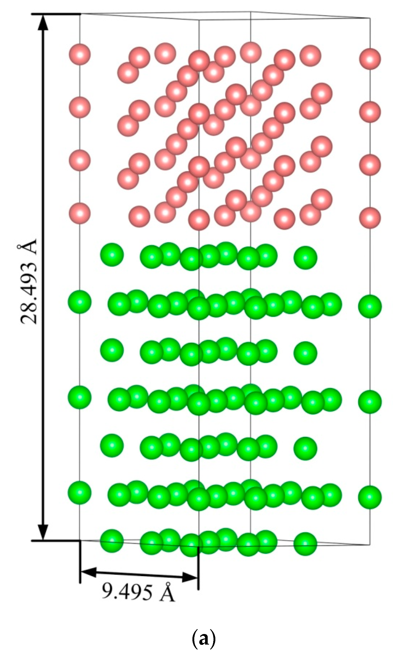
2.3. Ab Initio Calculations

Ab initio calculations were carried out within density functional theory using the optimized norm-conserving Vanderbilt pseudopotential method [44], as implemented in the ABINIT code [45,46]. The generalized gradient approximation (GGA) in the form of Perdew, Burke, and Ernzerhof [47] was used to describe the exchange and correlation effects. The cutoff energy for the plane wave basis was set to 15 Ha in the structural optimization. The atoms in the system were assumed to be in the equilibrium configuration when the force on each atom was below 10−3 Ha/bohr.
The present calculations were performed for pure Zr and Nb, Zr36H and Nb36H solid solutions with hydrogen in tetrahedral or octahedral interstitial sites (Figure 1), Zr63Nb40, and Zr63Nb40H slabs (Figure 2). The interface in Zr63Nb40 slab was formed by Zr (002) and Nb (111) surfaces. The Zr and Nb slabs consist of 7 and 10 atom monolayers, respectively. In Zr36H, Nb36H, and Zr63Nb40H systems H atom is located in the either tetrahedral (T) or octahedral (O) interstitial sites. For a more convenient discussion of results, the T and O sites in Figure 2b,c are enumerated. To carry out the structural optimization and relaxation of the system considered, a cell with 36 Zr or 36 Nb atoms was adopted, and the k meshes were chosen to be 3 × 3 × 3 for the hcp and bcc structures. For multilayer structures Zr63Nb40, k meshes were chosen 3 × 3 × 1.
To analyze the structural stability of the systems under consideration, the binding energy of hydrogen in metals was calculated:
Eb = E(Zr36) + 1/2 × E(H2) − E(Zr36H),
Eb = E(Nb36) + 1/2 × E(H2) − E(Nb36H),
Eb = E(Zr63Nb40) + 1/2 × E(H2) − E(Zr63Nb40H).
Here E(Zr36) and E(Nb36) are the energy of pure zirconium and niobium in the presence of 36 zirconium/niobium atoms in the supercell; E(H2) is the energy of the hydrogen molecule; E(Zr63Nb40) is the energy of the multilayer structure; E(Zr36) and E(Zr36H)are the energies of the zirconium lattice without and with hydrogen atoms, respectively; E(Nb36) and E(Nb36H) are the energies of the niobium lattice without and with hydrogen atoms, respectively; and E(Zr63Nb40H) is the energy of the multilayer structure when there is a hydrogen atom in it.

3. Results and Discussion

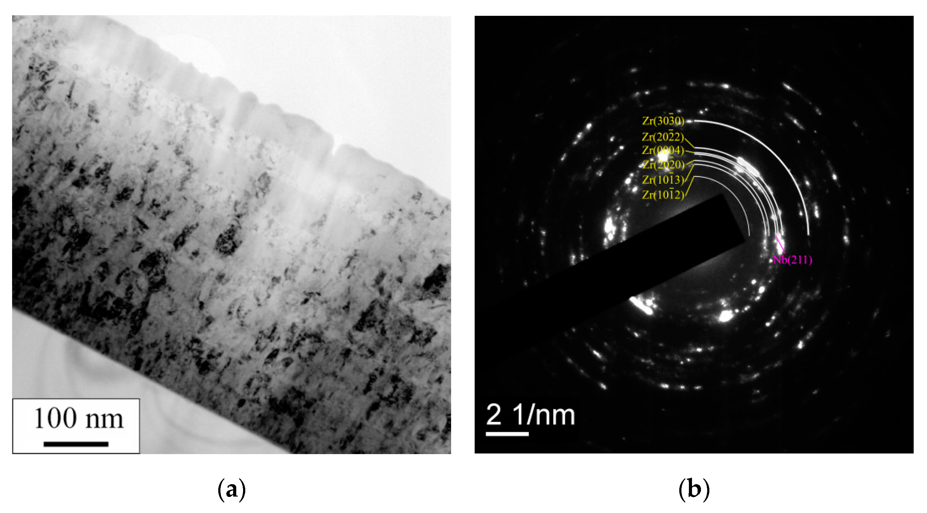
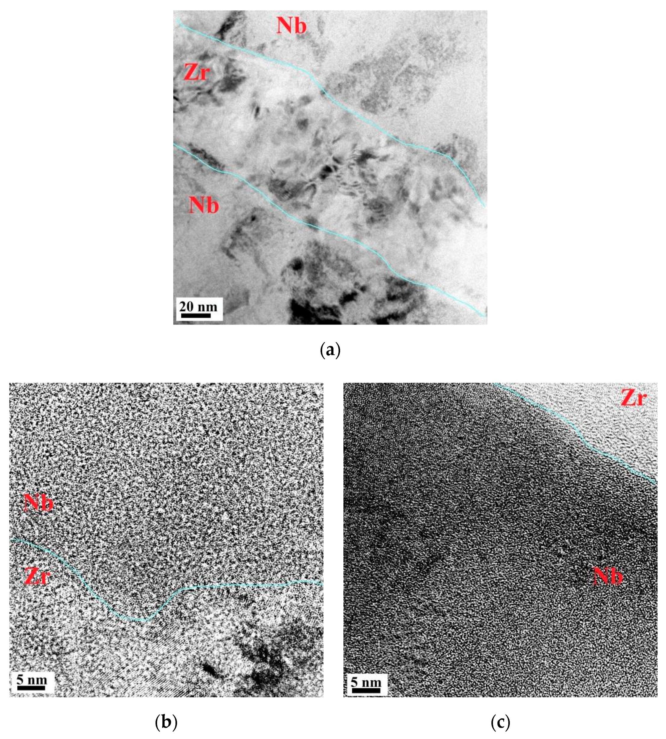
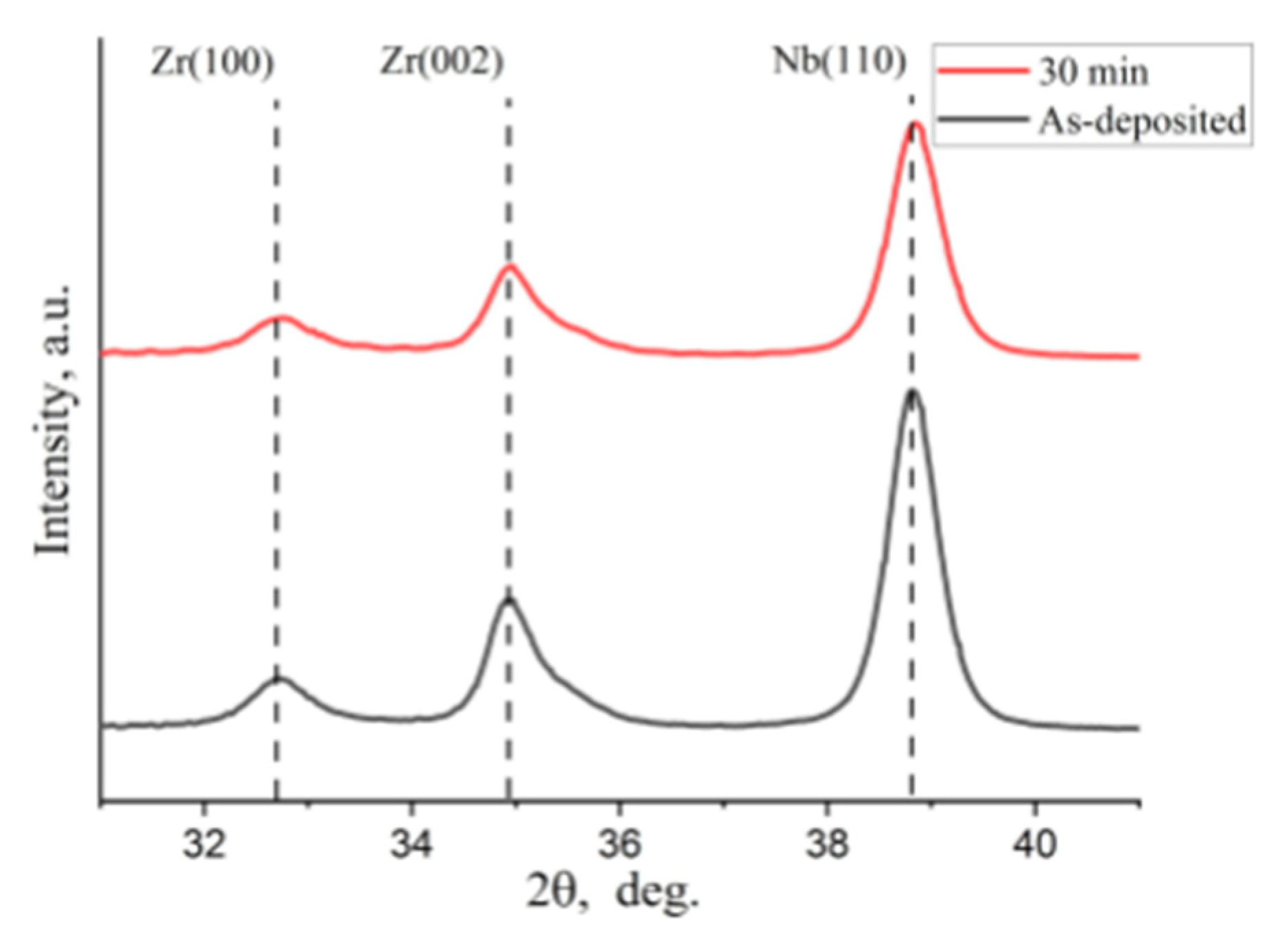
3.1. Microstructure of As-Deposited Zr/Nb Multilayer Coatings

Figure 3a demonstrates a STEM image of as-deposited Nb/Zr NMC cross-section.
It is clearly seen that a structure with alternating layers with a thickness of 100 ± 20 nm was obtained as a result of deposition. According to EDS data, the formed structure is represented by layers of zirconium and niobium with clearly distinguishable boundaries (Figure 3b,c). A more detailed study of the transverse sections of the as-deposited Zr/Nb NMC was carried out using transmission electron microscopy (Figure 4).
The corresponding selected area electron diffraction patterns (SAED) (Figure 4b) show an appreciable number of reflections distributed over a circle. The SAED patterns contain reflections from the different planes of the α phase of Zr and reflections of the Nb(211)β plane. The microstructure of each Zr and Nb layer is represented by nanoscale columnar grains, the average size of which varies from 20 to 50 nm. Grains in layers grow perpendicular to the substrate (Figure 4a). High-resolution TEM micrographs show an incoherent interface between Zr and Nb (Figure 5).
Figure 6 presents the diffraction patterns for as-deposited and irradiated Zr/Nb NMC obtained for samples’ surface.
Diffraction analysis showed that Zr layers are more susceptible to the formation of macro- and microstrains during deposition and irradiation. It can be seen from the pattern that the diffraction peaks are considerably broad, and values of full width on half maxima (FWHM) for Zr(100) and Zr(002) peaks are larger than for Nb (110), 0.9° and 0.67° against 0.58°. Peak broadening is usually attributed to large microstrain and small coherent diffraction domain size. For as-deposited Zr layers, the calculated microstrain and coherent diffraction domain sizes were 0.0073 and 9.9 ± 2.5 nm. Due to the high (110) texture of Nb layers, it is impossible to separate the contribution of microstrain and coherent diffraction domain size to peak broadening. Structural analysis from diffraction data revealed the presence of distortions in the crystal lattice, indicating macrostrains in as-deposited and irradiated Zr/Nb NMC. Macrostrains are especially pronounced for Zr layers; the hexagonal lattice parameters for as-deposited NMC were the following: a = 3.162 Å, c = 5.129 Å, which is 2.2% and 0.4% lesser than ideal lattice parameters for bulk Zr (a = 3.232 Å, c = 5.147 Å) [48]. For Nb layers, cubic a parameter was 3.278 Å (0.9% lesser than ideal a = 3.306 Å [49]). After 30 min of irradiation, minor changes in the diffraction pattern were noticed. A slight decrease in the lattice parameters was observed for the Zr and Nb layers, the values of which are as follows: a = 3.158 Å and c = 5.126 Å for Zr, and a = 3.276 Å for Nb. Additionally, an increase in FWHM value was noticed for Zr(100) to 1.07°, for Zr(002) to 0.7°, and for Nb(110) to 0.6°. Thus, for irradiated Zr layers, microstrain increased to 0.008, and coherent diffraction domain size decreased to 9.1 ± 2.4 nm.

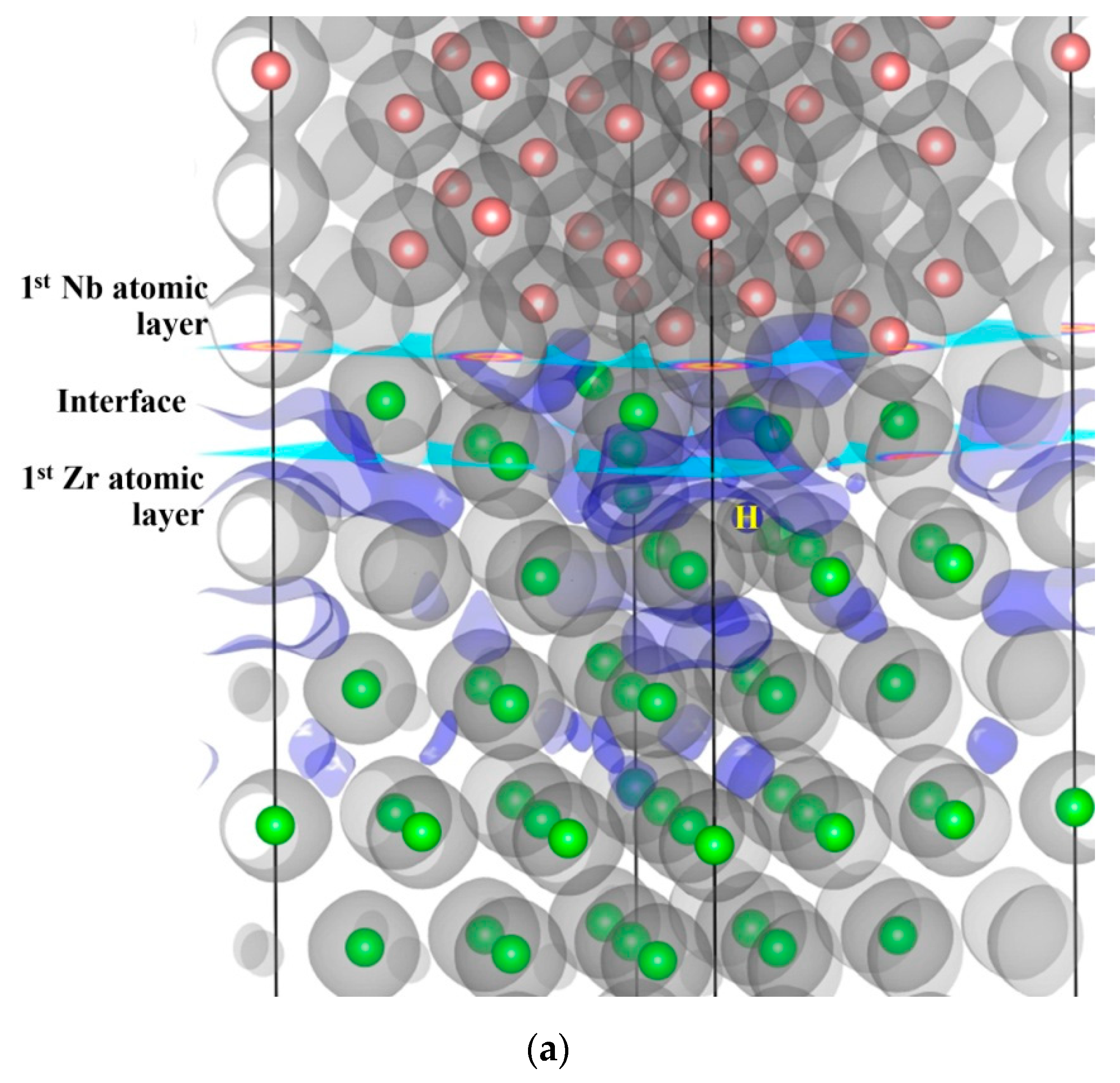
3.2. First-Principles Calculations of Zr/Nb Multilayer Coatings

The calculated lattice parameters of pure Zr and Nb, Zr36H, and Nb36H solid solutions are presented in Table 1. These theoretical results are in good agreement with the results of experiments and previous theoretical works [22,23]. To form the supercell of Zr63Nb40 slab, we decreased the theoretical lattice parameters of pure Nb and increased the lattice parameters of pure Zr until the total supercell energy became minimal. As a result, the supercell Zr slab have parameters a = 3.165 Å and c = 5.160 Å, and the Nb slab have parameter a = 3.341 Å. The distance between the Zr (002) and Nb (111) atomic layers in the interface was optimized. The equilibrium distance is equal to 2.215 Å, which is slightly lower than the result obtained in the previous theoretical work [24]. Finally, the atom positions in the three Zr and five Nb atomic layers nearest to the interface were relaxed. It was found that the Zr atom shifts near the interface are significantly higher than the Nb atom shifts. For example, the maximum atom shifts in the first Zr and Nb atomic layers are 1.090 Å and 0.348Å, respectively. In the second Zr and Nb atomic layers, these shifts reach 0.869 Å and 0.229Å, respectively. The Zr and Nb atom shift values in other relaxed atomic layers are close to each otherand do not exceed 0.2 Å. This fact partially explains microstrain studies’ results: the Zr layer’s deformation is noticeably higher than that of the Nb.
The results of the hydrogen binding energy calculation in solid solutions and slab are presented in Table 2. The calculated hydrogen binding energy in zirconium is in good agreement with the results of previous theoretical work [22].
The maximum binding energy corresponds to the tetrahedral coordination of a hydrogen atom in both metals. It should be noted that in the case when the hydrogen atom is located in the O site of niobium, even its small displacements from the center of this site lead to the appearance of force that shifts the H atom to the nearest T site. This indicates the instability of this hydrogen position in niobium. As a result, in the Zr63Nb40H slab, we considered the location of an H atom in T and O sites of the Zr layer and in T sites of the Nb layer. The maximal value of hydrogen binding energy is observed in the T6 site in the first Zr atomic layers (see Figure 2c). It should be noted that the binding energy values are varied in a wide range for each metal atomic layer. In the first Zr atomic layers, this range is from 0.653 to 1.035 eV for tetrahedral coordination and from 0.758 to 0.970 eV for octahedral coordination of hydrogen atoms. However, the average value of hydrogen binding energy per metal atomic layer is decreased with an increase in distance between the atomic layer and interface (Figure 7). In the Zr layer, this decrease is slower than in the Nb layers.

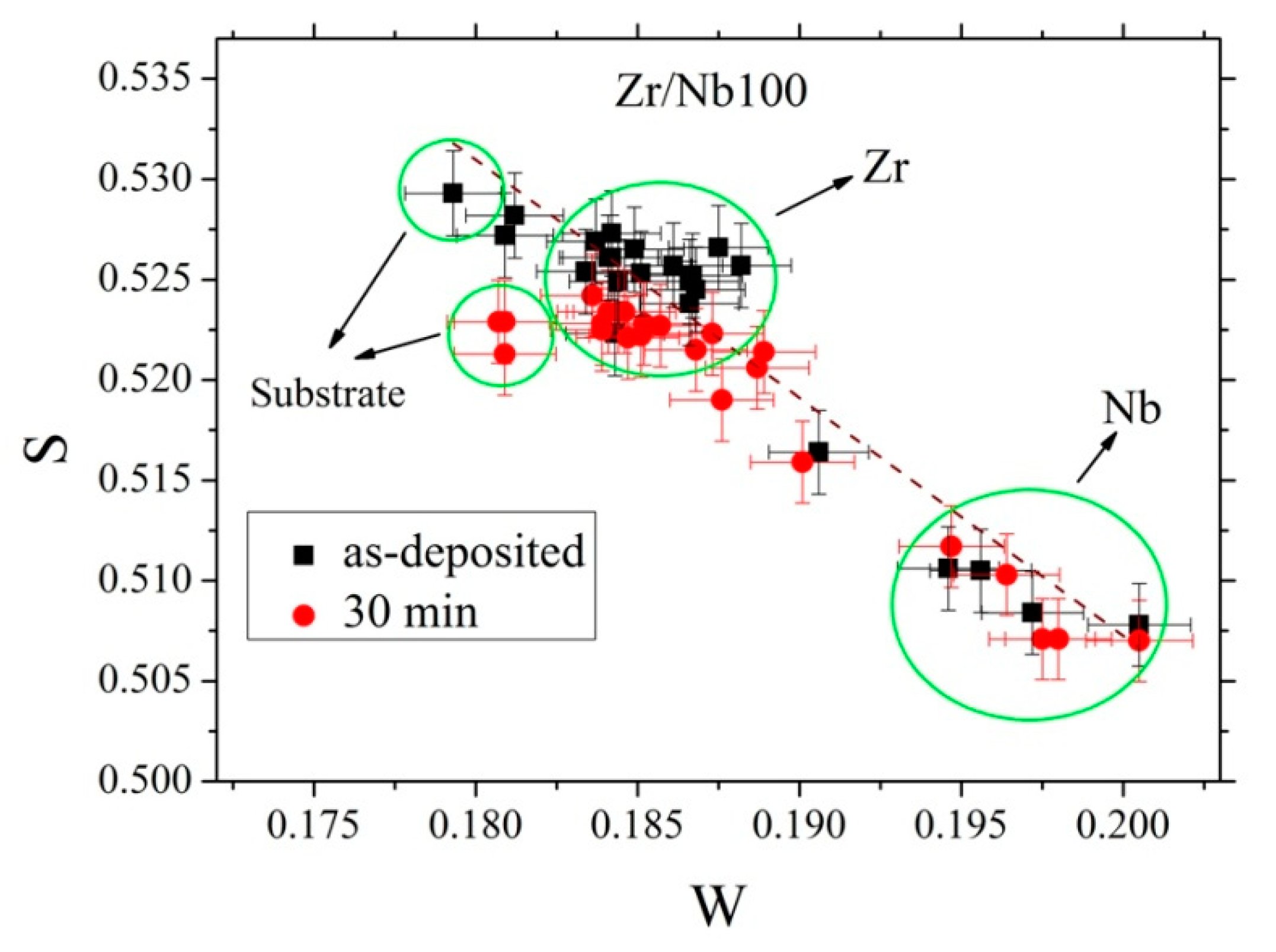
3.3. Depth Profiling and Defect Characterization of Zr/Nb Nanoscale Multilayers after H+ Irradiation

Figure 8 presents the element distribution profiles for as-deposited and irradiated Zr/Nb NMC.
Figure 8 shows a GD-OES profile of the Zr/Nb multilayer system consisting of five Zr-layers approximately 80 ± 10 nm thick and five Nb-layers with 100 ± 10 nm thickness, which agrees well with the STEM results (Figure 3). The transient areas between layers present in the GD-OES profiles are related to the crater effect [36,50,51]. The Zr/Nb interface near the Si substrate was not considered. Trace amounts of hydrogen are present in the unirradiated material, and hydrogen is mainly localized in the Nb/Zr interface area. The main changes in the relative GD-OES curves are associated with the accumulation of hydrogen ions. The hydrogen concentration maximum occurs at a depth of ~800 nm, which corresponds to the Bragg peak for H+ ions, according to SRIM calculations [15]. The hydrogen distribution has a multimodal character, with local maxima of hydrogen concentration observed at the Nb/Zr interfaces, while the accumulation on Zr/Nb is much lower. The intensity ratio of the H line for the Nb/Zr and Zr/Nb interfaces is approximately 1:2, and the hydrogen concentration at the Zr/Nb interface is almost equal to the hydrogen concentration in the bulk of niobium. Moreover, hydrogen predominantly localizes in the zirconium layers, which agrees well with the first-principles calculations (Figure 7), which showed that near the Zr/Nb interface, the hydrogen binding energy in the zirconium atomic layers is significantly higher than in the niobium atomic layers.
The DBS-VEP analysis of the annihilation line in Zr/Nb NMCs is shown in Figure 9.
Because the depth of positron implantation nonlinearly changes with increasing energy, only the first layers (from the top surface) of niobium and zirconium have been entirely examined. The S parameter for niobium is about 0.507 ± 0.004 and increases when positrons annihilate in Zr. In unirradiated samples at positron energies from 4 to 26 keV, the S parameter value is about 0.525 ± 0.005. The W parameter also changes weakly in this energy range, which shows that positrons beginning from energy 4 keV start annihilate in the zirconium area. The dependence S = f(W), shown in Figure 10, also confirms this assumption.
The number of positron annihilation in Zr may be higher due to the selective positron trapping [52] in the multilayer system caused by the positron affinity of zirconium which is 26% bigger than for niobium [53]. However, suppose the thickness of individual layers is about 100 ± 20 nm, and the average positron diffusion length is comparable with nanocrystallites’ size-32 ± 15 nm. In that case, it is unlikely that all positrons annihilate only in Zr. Therefore, the obtained value of 0.525 ± 0.005 should be assigned to the mixed state of the S parameter value of pure Zr and Nb, which is closer to pure Zr value due to lower Nb positron affinity.
To reveal the influence of the Zr/Nb interface on peculiarities of the distribution of positron annihilation, a comparative analysis of the electron density distribution in the interface vicinity of Zr63Nb40 slabs was performed. Figure 11 shows that the electron density distribution near the interface is not homogeneous on both the Zr and Nb layers.
There are areas of a reduced electron density (*) in the Zr atomic layers near the interface. With increasing distance from the interface, the number of these areas increases, but their size decreases. The niobium atomic layers are almost entirely devoid of such areas. The appearance of such areas in the Zr atomic layers is due to high Zr atom shifts to the interface. In the fourth Zr atomic layer, where atoms are located at the ideal hcp lattice site, such areas are not observed. Thus, positron annihilation near the interfaces will mainly occur in the zirconium area. A detailed study of reduced electron density areas requires a positron lifetime spectroscopy analysis.
After irradiation with H+ ions for 30 min in Zr/Nb NMC, a slight decrease in the S parameter and W parameter growth in the Zr and Nb first layers are observed. That indicates a reduction of free volume in these layers. Moreover, in the Zr layer, these changes are more pronounced. A further increase in the positron implantation depth does not lead to significant variations in the DBS parameters. The indicated relative changes in DBS parameters (S↑W↓) are observed during hydrogen-vacancy complexes formation in hcp materials [54,55]. However, in this case, S0 < SH < SVAC, where S0 corresponds to the initial material, SH to the hydrogenated material, and SVAC to the material with vacancies. It is also shown in [55] that the S parameter decreases and W increases compared to the initial value is possible with H accumulation in the material.
In order to reveal the influence of hydrogen on the interaction between zirconium and niobium atoms in the interface, a comparative analysis of the electron density distribution in the interface vicinity of Zr63Nb40H slabs with H atom in the most energetically favorable octahedral (O1) and tetrahedral (T6) positions was performed (Figure 12 and Figure 13).
Hydrogen placed at the favorable T6 (Figure 12) or O1 (Figure 13) positions has a minor effect on the electron density distribution near the Zr/Nb interface. The reduced electron density area configuration is changed. The presence of hydrogen atoms in O1 or T6 position increases the electron density by ~5–10% of this area in the Zr and Nb atomic layers nearest to the interface and slightly reduces the size of these areas in the second and third Zr atomic layers. Such variations will not significantly affect the positron annihilation parameters shown in Figure 9 and Figure 10. All experimental points on the S = f(W) dependence before and after irradiation are on the same straight line, indicating one prevailing type of positron trapping—the free volume near the interface in the vicinity of zirconium.

4. Conclusions

In this work, a Zr/Nb nanoscale multilayer system before and after H+ irradiation was investigated by combining different experimental techniques with first-principles calculations. A multilayer Zr/Nb system with individual layer thicknesses of 80 ± 10 nm and 100 ± 10 nm for Zr and Nb, respectively, was formed using magnetron sputtering. Microstructures are characterized by nanoscale columnar grains with an average size from 20 to 50 nm. XRD analyses revealed the presence of macro-and microstrains in the Zr/Nb NMC. These strains are noticeably higher for Zr layers because, according to the first-principles calculations, the Zr atom shifts from the ideal lattice site near the interface are significantly higher than Nb atom shifts. Irradiation with 900 keV H+ ions for 30 min leads to an intense accumulation of H in the metal atomic layer near the Nb/Zr interfaces due to the highest hydrogen binding energy. The decrease in the average hydrogen binding energy per metal atomic layer with an increase in distance between the atomic layer and interface is slower in the Zr layer than in the Nb layer. That clearly explains the predominant hydrogen localization in Zr layers and increasing microstrains observed by GD-OES and XRD methods. The DBS-VEP analysis results do not indicate an increase in defect concentration after H+ irradiation across the coating thickness. Before and after irradiation, positrons annihilate near the interfaces, mainly in the Zr vicinity, due to high positron affinity and the presence of reduced electron density area due to high Zr atom shifts to the interface.

Author Contributions

R.L. made the organization of the experimental procedure and preparation of the manuscript. L.S. conducted the first-principles calculations of the electronic structure. E.S. carried out microstructure analysis using TEM. N.P. performed and analyzed STEM micrographs. A.L. examined samples using the GD-OES method. D.K. provided SRIM calculations and XRD analysis. K.S. performed layer-by-layer analysis using positron spectroscopy methods. S.O. made samples and preliminary data for calculations. V.U. carried out a comprehensive analysis of the received data and prepared the manuscript for publication. All authors have read and agreed to the published version of the manuscript.

Funding

This work was funded by the Russian Science Foundation, research project No. 20-79-10343.

Institutional Review Board Statement

Not applicable.

Informed Consent Statement

Not applicable.

Data Availability Statement

Data is contained within the article.

Acknowledgments

The authors are grateful to Innovation Centre for Nanomaterials and Nanotechnologies of Tomsk Polytechnic University for TEM/SEM preparations and personally to the researcher Oleg Tolkachev. The preparation and adjustment of the used equipment are performed within the Competitiveness Enhancement Program of National Research Tomsk Polytechnic University.

Conflicts of Interest

The authors declare no conflict of interest.

References

  1. Bull, S.J. Size effects in the mechanical response of nanoscale multilayer coatings on glass. Thin Solid Film. 2014, 571, 290–295. [Google Scholar] [CrossRef] [Green Version]
  2. Fazel, Z.A.; Elmkhah, H.; Fattah-Alhosseini, A.; Babaei, K.; Meghdari, M. Comparing electrochemical behavior of applied CrN/TiN nanoscale multilayer and TiN single-layer coatings deposited by CAE-PVD method. J. Asian Ceram. Soc. 2020, 8, 510–518. [Google Scholar] [CrossRef] [Green Version]
  3. Contreras, E.; Galindez, Y.; Rodas, M.A.; Bejarano, G.; Gómez, M.A. CrVN/TiN nanoscale multilayer coatings deposited by DC unbalanced magnetron sputtering. Surf. Coat. Technol. 2017, 332, 214–222. [Google Scholar] [CrossRef]
  4. Chen, J.; Geng, M.; Li, Y.; Yang, Z.; Chai, Y.; He, G. Erosion Resistance and Damage Mechanism of TiN/ZrN Nanoscale Multilayer Coating. Coatings 2019, 9, 64. [Google Scholar] [CrossRef] [Green Version]
  5. Puchi-Cabrera, E.S.; Staia, M.H.; Iost, A. Modeling the composite hardness of multilayer coated systems. Thin Solid Film. 2015, 578, 53–62. [Google Scholar] [CrossRef] [Green Version]
  6. Wang, L.; Wang, M.; Chen, H. Electrochemical Corrosion Behavior of TiAlN/CrN Nanoscale Multilayer Coatings by Multi-Arc Ion Plating in 3.5% NaCl Solution. Corrosion 2020, 76, 628–638. [Google Scholar] [CrossRef]
  7. Demkowicz, M.J.; Hoagland, R.G.; Hirth, J.P. Interface structure and radiation damage resistance in Cu-Nb multilayer nanocomposites. Phys. Rev. Lett. 2008, 100, 136102. [Google Scholar] [CrossRef]
  8. Gao, Y.; Yang, T.; Xue, J.; Yan, S.; Zhou, S.; Wang, Y.; Kwok, D.T.K.; Chu, P.K.; Zhang, Y. Radiation tolerance of Cu/W multilayered nanocomposites. J. Nucl. Mater. 2011, 413, 11–15. [Google Scholar] [CrossRef]
  9. Wei, Q.M.; Li, N.; Mara, N.; Nastasi, M.; Misra, A. Suppression of irradiation hardening in nanoscale V/Ag multilayers. Acta Mater. 2011, 59, 6331–6340. [Google Scholar] [CrossRef]
  10. Demkowicz, M.J.; Wang, Y.Q.; Hoagland, R.G.; Anderoglu, O. Mechanisms of He escape during implantation in CuNb multilayer composites. In Nuclear Instruments and Methods in Physics Research Section B: Beam Interactions with Materials and Atoms; Elsevier: Amsterdam, The Netherlands, 2007; Volume 261, pp. 524–528. [Google Scholar]
  11. Ham, B.; Zhang, X. High strength Mg/Nb nanolayer composites. Mater. Sci. Eng. 2011, 528, 2028–2033. [Google Scholar] [CrossRef]
  12. Thorsen, P.A.; Bilde-Sørensen, J.B.; Singh, B.N. Bubble formation at grain boundaries in helium implanted copper. Scr. Mater. 2004, 51, 557–560. [Google Scholar] [CrossRef]
  13. Han, W.Z.; Demkowicz, M.J.; Fu, E.G.; Wang, Y.Q.; Misra, A. Effect of grain boundary character on sink efficiency. Acta Mater. 2012, 60, 6341–6351. [Google Scholar] [CrossRef]
  14. Chen, E.Y.; Deo, C.; Dingreville, R. Irradiation resistance of nanostructured interfaces in Zr-Nb metallic multilayers. J. Mater. Res. 2019, 34, 2239–2251. [Google Scholar] [CrossRef] [Green Version]
  15. Laptev, R.; Lomygin, A.; Krotkevich, D.; Syrtanov, M.; Kashkarov, E.; Bordulev, Y.; Siemek, K.; Kobets, A. Effect of Proton Irradiation on the Defect Evolution of Zr/Nb Nanoscale Multilayers. Metals 2020, 10, 535. [Google Scholar] [CrossRef] [Green Version]
  16. Frutos, E.; Callisti, M.; Karlik, M.; Polcar, T. Length-scale-dependent mechanical behaviour of Zr/Nb multilayers as a function of individual layer thickness. Mater. Sci. Eng. 2015, 632, 137–146. [Google Scholar] [CrossRef]
  17. Monclús, M.A.; Callisti, M.; Polcar, T.; Yang, L.W.; Molina-Aldareguía, J.M.; LLorca, J. Effect of layer thickness on the mechanical behaviour of oxidation-strengthened Zr/Nb nanoscale multilayers. J. Mater. Sci. 2018, 53, 5860–5878. [Google Scholar] [CrossRef] [Green Version]
  18. Li, N.; Mara, N.A.; Wang, Y.Q.; Nastasi, M.; Misra, A. Compressive flow behavior of Cu thin films and Cu/Nb multilayers containing nanometer-scale helium bubbles. Scr. Mater. 2011, 64, 974–977. [Google Scholar] [CrossRef]
  19. Fu, E.G.; Carter, J.; Swadener, G.; Misra, A.; Shao, L.; Wang, H.; Zhang, X. Size dependent enhancement of helium ion irradiation tolerance in sputtered Cu/V nanolaminates. J. Nucl. Mater. 2009, 385, 629–632. [Google Scholar] [CrossRef]
  20. Fu, E.G.; Li, N.; Misra, A.; Hoagland, R.G.; Wang, H.; Zhang, X. Mechanical properties of sputtered Cu/V and Al/Nb multilayer films. Mater. Sci. Eng. 2008, 493, 283–287. [Google Scholar] [CrossRef]
  21. Fu, E.G.; Misra, A.; Wang, H.; Shao, L.; Zhang, X. Interface enabled defects reduction in helium ion irradiated Cu/V nanolayers. J. Nucl. Mater. 2010, 407, 178–188. [Google Scholar] [CrossRef]
  22. Wang, F.; Gong, H.R. First principles study of various Zr–H phases with low H concentrations. Int. J. Hydrogen Energy 2012, 37, 12393–12401. [Google Scholar] [CrossRef]
  23. Ford, D.C.; Cooley, L.D.; Seidman, D.N. First-principles calculations of niobium hydride formation in superconducting radio-frequency cavities. Supercond. Sci. Technol. 2013, 26, 095002. [Google Scholar] [CrossRef] [Green Version]
  24. Sen, H.S.; Polcar, T. Vacancy-interface-helium interaction in Zr-Nb multi-layer system: A first-principles study. J. Nucl. Mater. 2019, 518, 11–20. [Google Scholar] [CrossRef]
  25. Callisti, M.; Lozano-Perez, S.; Polcar, T. Structural and mechanical properties of γ-irradiated Zr/Nb multilayer nanocomposites. Mater. Lett. 2016, 163, 138–141. [Google Scholar] [CrossRef] [Green Version]
  26. Callisti, M.; Karlik, M.; Polcar, T. Competing mechanisms on the strength of ion-irradiated Zr/Nb nanoscale multilayers: Interface strength versus radiation hardening. Scr. Mater. 2018, 152, 31–35. [Google Scholar] [CrossRef] [Green Version]
  27. Monclús, M.A.; Callisti, M.; Polcar, T.; Yang, L.W.; Llorca, J.; Molina-Aldareguía, J.M. Selective oxidation-induced strengthening of Zr/Nb nanoscale multilayers. Acta Mater. 2017, 122, 1–10. [Google Scholar] [CrossRef] [Green Version]
  28. Daghbouj, N.; Karlík, M.; Lörinčík, J.; Polcar, T.; Callisti, M.; Havránek, V. Effect of implantation of C, Si and Cu into ZrNb nanometric multilayers. In Proceedings of the METAL 2019—28th International Conference on Metallurgy and Materials, Brno, Czech Republic, 22–24 May 2019; TANGER Ltd.: Ostrava, Czech Republic, 2019; pp. 944–949. [Google Scholar]
  29. Daghbouj, N.; Callisti, M.; Sen, H.S.; Karlik, M.; Čech, J.; Vronka, M.; Havránek, V.; Čapek, J.; Minárik, P.; Bábor, P.; et al. Interphase boundary layer-dominated strain mechanisms in Cu+ implanted Zr-Nb nanoscale multilayers. Acta Mater. 2021, 202, 317–330. [Google Scholar] [CrossRef]
  30. Ziegler, J.F.; Ziegler, M.D.; Biersack, J.P. SRIM—The stopping and range of ions in matter (2010). In Nuclear Instruments and Methods in Physics Research Section B: Beam Interactions with Materials and Atoms; Elsevier: Amsterdam, The Netherlands, 2010; Volume 268, pp. 1818–1823. [Google Scholar]
  31. Syrtanov, M.; Garanin, G.; Kashkarov, E.; Pushilina, N.; Kudiiarov, V.; Murashkina, T. Laboratory X-ray Diffraction Complex for In Situ Investigations of Structural Phase Evolution of Materials under Gaseous Atmosphere. Metals 2020, 10, 447. [Google Scholar] [CrossRef] [Green Version]
  32. Kraus, W.; Nolze, G. Powder Cell—A program for the representation and manipulation of crystal structures and calculation of the resulting X-ray powder patterns. J. Appl. Cryst. 1996, 29, 301–303. [Google Scholar] [CrossRef]
  33. Krysina, O.; Ivanov, Y.; Prokopenko, N.; Shugurov, V.; Tolkachev, O.; Petrikova, E. Plasma assistance effect on the example of Zrn-based coatings deposited by vacuum-arc method at the addition of NB. In Proceedings of the Proceedings—2020 7th International Congress on Energy Fluxes and Radiation Effects, EFRE 2020, Tomsk, Russia, 14–26 September 2020; Institute of Electrical and Electronics Engineers Inc.: Piscataway, NJ, USA, 2020; pp. 551–555. [Google Scholar]
  34. Priamushko, T.; Mikhaylov, A.; Babikhina, M.; Kudiiarov, V.; Laptev, R. Glow Discharge Optical Emission Spectrometer Calibration Using Hydrogenated Zr-2.5Nb Alloy Standard Samples. Metals 2018, 8, 372. [Google Scholar] [CrossRef] [Green Version]
  35. Mikhaylov, A.A.; Priamushko, T.S.; Babikhina, M.N.; Kudiiarov, V.N.; Heller, R.; Laptev, R.S.; Lider, A.M. Hydrogen calibration of GD-spectrometer using Zr-1Nb alloy. Appl. Surf. Sci. 2018, 432, 85–89. [Google Scholar] [CrossRef]
  36. Shulepov, I.; Lomygin, A.; Laptev, R.; Kashkarov, E.; Syrtanov, M. Correction of the distribution profiles of the intensities of elements considering the uneven dispersion of the glow-discharge optical emission spectrometer for multilayer coatings analysis. In Proceedings of the Proceedings—2020 7th International Congress on Energy Fluxes and Radiation Effects, EFRE 2020, Tomsk, Russia, 14–26 September 2020; Institute of Electrical and Electronics Engineers Inc.: Piscataway, NJ, USA, 2020; pp. 1155–1159. [Google Scholar]
  37. Horodek, P.; Kobets, A.G.; Meshkov, I.N.; Sidorin, A.A.; Orlov, O.S. Slow positron beam at the JINR, Dubna. Nukleonika 2015, 60, 725–728. [Google Scholar] [CrossRef] [Green Version]
  38. Horodek, P.; Bugdol, M.; Kobets, A.G.; Meshkov, I.N.; Orlov, O.S.; Rudakov, A.Y.; Sidorin, A.A.; Yakovenko, S.L. Development of positron annihilation spectroscopy at LEPTA facility. Phys. Part. Nucl. Lett. 2014, 11, 708–712. [Google Scholar] [CrossRef] [Green Version]
  39. Krause-Rehberg, R.; Leipner, L. Positron Annihilation in Semiconductors; Solid-State Sciences; Springer: Berlin/Heidelberg, Germany, 1999; Volume 127, ISBN 978-3-540-64371-5. [Google Scholar]
  40. Laptev, R.S.; Lider, A.M.; Bordulev, Y.S.; Kudiiarov, V.N.; Garanin, G.V.; Wang, W.; Kuznetsov, P.V. Investigation of defects in hydrogen-saturated titanium by means of positron annihilation techniques. In Proceedings of the DSL 2014—10th International Conference on Diffusion in Solids and Liquids, Paris, France, 23–27 June 2014; Trans Tech Publications Ltd.: Stafa-Zurich, Switzerland, 2015; Volume 365, pp. 232–236. [Google Scholar]
  41. Baranowski, A.; Kostrzewa, M.; Szuszkiewicz, M. Studying of nickel alloys with 1 at.% of Ge, Zn, In, Zr, and Pb by positron annihilation methods. Acta Phys. Pol. 2001, 99, 329–336. [Google Scholar] [CrossRef]
  42. Uedono, A.; Ikeuchi, K.; Otsuka, T.; Yamabe, K.; Eguchi, K.; Takayanagi, M.; Ishibashi, S.; Ohdaira, T.; Muramatsu, M.; Suzuki, R. Vacancy-impurity complexes in polycrystalline Si used as gate electrodes of HfSiON-based metal-oxide-semiconductors probed using monoenergetic positron beams. J. Appl. Phys. 2006, 100, 034509. [Google Scholar] [CrossRef]
  43. Kuznetsov, P.V.; Mironov, Y.P.; Tolmachev, A.I.; Bordulev, Y.S.; Laptev, R.S.; Lider, A.M.; Korznikov, A.V. Positron spectroscopy of defects in submicrocrystalline nickel after low-temperature annealing. Phys. Solid State 2015, 57, 219–228. [Google Scholar] [CrossRef]
  44. Hamann, D.R. Optimized norm-conserving Vanderbilt pseudopotentials. Phys. Rev. B Condens. Matter Mater. Phys. 2013, 88, 085117. [Google Scholar] [CrossRef] [Green Version]
  45. Gonze, X.; Amadon, B.; Antonius, G.; Arnardi, F.; Baguet, L.; Beuken, J.M.; Bieder, J.; Bottin, F.; Bouchet, J.; Bousquet, E.; et al. The ABINIT project: Impact, environment and recent developments. Comput. Phys. Commun. 2020, 248, 107042. [Google Scholar] [CrossRef]
  46. Romero, A.H.; Allan, D.C.; Amadon, B.; Antonius, G.; Applencourt, T.; Baguet, L.; Bieder, J.; Bottin, F.; Bouchet, J.; Bousquet, E.; et al. ABINIT: Overview and focus on selected capabilities. J. Chem. Phys. 2020, 152, 124102. [Google Scholar] [CrossRef] [PubMed]
  47. Perdew, J.P.; Burke, K.; Ernzerhof, M. Generalized gradient approximation made simple. Phys. Rev. Lett. 1996, 77, 3865–3868. [Google Scholar] [CrossRef] [Green Version]
  48. Zhao, Y.; Li, H.; Huang, Y. The structure, mechanical, electronic and thermodynamic properties of bcc Zr-Nb alloy: A first principles study. J. Alloys Compd. 2021, 862, 158029. [Google Scholar] [CrossRef]
  49. Roberge, R. Lattice parameter of niobium between 4. 2 and 300K. J. Less-Common Met. 1975, 40, 1. [Google Scholar] [CrossRef]
  50. Liu, Y.; Yu, W.H.; Wang, J.Y. A model for quantification of GDOES depth profiles. Vacuum 2015, 113, 5–10. [Google Scholar] [CrossRef]
  51. Liu, Y.; Jian, W.; Wang, J.Y.; Hofmann, S.; Shimizu, K. Quantitative reconstruction of the GDOES sputter depth profile of a monomolecular layer structure of thiourea on copper. Appl. Surf. Sci. 2015, 331, 140–149. [Google Scholar] [CrossRef]
  52. Qi, N.; Zhang, H.X.; Chen, Z.Q.; Ren, F.; Zhao, B.; Jiang, M.; Uedono, A. Selective trapping of positrons by Ag nanolayers in a V/Ag multilayer system. AIP Adv. 2020, 10, 035012. [Google Scholar] [CrossRef]
  53. Puska, M.J.; Lanki, P.; Nieminen, R.M. Positron affinities for elemental metals. J. Phys. Condens. Matter 1989, 1, 6081–6094. [Google Scholar] [CrossRef]
  54. Laptev, R.S.; Kudiiarov, V.N.; Bordulev, Y.S.; Mikhaylov, A.A.; Lider, A.M. Gas-phase hydrogenation influence on defect behavior in titanium-based hydrogen-storage material. Prog. Nat. Sci. Mater. Int. 2017, 27, 105–111. [Google Scholar] [CrossRef]
  55. Bordulev, I.; Kudiiarov, V.; Svyatkin, L.; Syrtanov, M.; Stepanova, E.; Čížek, J.; Vlček, M.; Li, K.; Laptev, R.; Lider, A. Positron annihilation spectroscopy study of defects in hydrogen loaded Zr-1Nb alloy. J. Alloys Compd. 2019, 798, 685–694. [Google Scholar] [CrossRef]
Figure 1. The interstitial sites in the (a) zirconium and (b) niobium supercells. Tetrahedral sites are blue, and octahedral sites are grey.
Metals 11 00627 g001
Figure 2. The supercell of Zr63Nb40 multilayer structures (a) and positions of the considered interstitial sites in the Zr63Nb40 supercell: (b) in Nb layer, (c) in Zr layer. Zirconium atoms are green, niobium atoms are pink, octahedral sites are grey, and tetrahedral sites are blue.
Metals 11 00627 g002aMetals 11 00627 g002b
Figure 3. Cross-section STEM image (a) and EDS-mapping of Zr (yellow) (b) and Nb (pink) (c) layers of the as-deposited Zr/Nb NMC.
Metals 11 00627 g003
Figure 4. Cross-sectional bright-field TEM image showing the microstructure of the Zr/Nb multilayers (a) and the corresponding SAED (b).
Metals 11 00627 g004
Figure 5. Cross-sectional HRTEM images of the Zr/Nb multilayer (a) bright-field image of the Zr/Nb multilayers (b) corresponding fast Fourier transform (FFT) for the HRTEM images of the Zr/Nb (c) and the Nb/Zr interfaces. The blue lines show the interface between Zr and Nb.
Metals 11 00627 g005
Figure 6. Diffraction patterns for as-deposited and irradiated Zr/Nb NMC.
Metals 11 00627 g006
Figure 7. The calculated dependence of the average value of hydrogen binding energy on the atomic layer number. The pink dotted line indicates the hydrogen binding energy in the T sites of the pure Nb, and the green dotted line indicates the average value of hydrogen binding energy in the pure Zr.
Metals 11 00627 g007
Figure 8. GD-OES profiles of element distribution for Zr/Nb NMC: (a) as-deposited, (b) H+ irradiated.
Metals 11 00627 g008
Figure 9. DBS-VEP depth profile of the S (a) and W (b) parameters for Zr/Nb 100. The S parameter stands for positron annihilation with low momentum electrons (it increases with defects concentration and is higher for Zr than Nb), and W is responsible for positron annihilation with high momentum electrons.
Metals 11 00627 g009
Figure 10. Dependence of S = f(W) for irradiated and as-deposited Zr/Nb 100. The dashed line indicates the approximating curve S = 0.744–1.185 W.
Metals 11 00627 g010
Figure 11. Electron density distribution in the interface vicinity of Zr63Nb40 slab (a) and in the first Zr (b) and Nb (c) atomic layers. The blue and gray isosurfaces in panel (a) correspond to a charge density of 0.02 and 0.05 electrons/Bohr3, respectively. The areas of a reduced electron density in the Zr (b) and Nb (c) atomic layers are marked with (*). Color gradation scale in the (b,c) panels is given in electrons/Bohr3 units.
Metals 11 00627 g011
Figure 12. Electron density distribution in the interface vicinity of Zr63Nb40H slab with H atom in tetrahedral (T6) site (a) and in the first Zr (b) and Nb (c) atomic layers. The blue and gray isosurfaces in panel (a) correspond to a charge density of 0.02 and 0.05 electrons/Bohr3, respectively. The areas of a reduced electron density in the Zr (b) and Nb (c) atomic layers are marked with (*). Color gradation scale in the (b,c) panels is given in electrons/Bohr3 units.
Metals 11 00627 g012aMetals 11 00627 g012b
Figure 13. Electron density distribution in the interface vicinity of Zr63Nb40H slab with H atom in octahedral (O1) site (a) and in the first Zr (b) and Nb (c) atomic layers. The blue and gray isosurfaces in panel (a) correspond to a charge density of 0.02 and 0.05 electrons/Bohr3, respectively. The areas of a reduced electron density in the Zr (b) and Nb (c) atomic layers are marked with (*). Color gradation scale in the (b,c) panels is given in electrons/Bohr3 units.
Metals 11 00627 g013aMetals 11 00627 g013b
Table 1. The theoretical lattice parameters of pure Zr and Nb, Zr36H and Nb36H solid solutions.
SystemLattice Parameters, (Å)
Actual WorkOther Calculations
Zra = 3.228a = 3.213 [22]
c = 5.195c = 5.157 [22]
Zr36H
(H atom in T site)
a = 3.229a = 3.245 [22]
c = 5.203c = 5.218 [22]
Zr36H
(H atom in O site)
a = 3.228a = 3.240 [22]
c = 5.199c = 5.203 [22]
Nba = 3.292a = 3.32 [23]
Nb36H
(H atom in T site)
a = 3.294
Nb36H
(H atom in O site)
a = 3.294
Table 2. The hydrogen binding energy in Zr36H and Nb36H solid solutions, Zr63Nb40H slab.
SiteEb, (eV)SiteEb, (eV)SiteEb, (eV)SiteEb, (eV)
Zr36H Solid SolutionNb36H Solid Solution
T0.459
0.45 [22]
O0.409
0.35 [22]
T0.380O0.160
Zr63Nb40H slab
O10.970O40.765O70.731T210.768
O20.758O50.769O80.748T220.713
O30.800O60.762O90.672T230.511
T11.007T80.786T140.760T240.554
T20.822T90.809T150.697T250.498
T30.656T100.551T160.649T260.349
T40.816T110.963T170.513T270.517
T50.788T120.832T180.752T280.477
T61.035T130.655T190.644T290.486
T70.653--T200.618T300.488
Publisher’s Note: MDPI stays neutral with regard to jurisdictional claims in published maps and institutional affiliations.

