Article

Bias Polarity Dependent Threshold Switching and Bipolar Resistive Switching of TiN/TaOx/ITO Device

Department of Electronics and Electrical Engineering, Dongguk University, Seoul 04620, Korea
*
Author to whom correspondence should be addressed.
Metals 2021, 11(10), 1531; https://doi.org/10.3390/met11101531
Submission received: 29 August 2021 / Revised: 17 September 2021 / Accepted: 24 September 2021 / Published: 26 September 2021
(This article belongs to the Special Issue Metal Oxides Characterization for Emerging Memory Device Applications)

Abstract

:
In this work, we demonstrate the threshold switching and bipolar resistive switching with non-volatile property of TiN/TaOx/indium tin oxide (ITO) memristor device. The intrinsic switching of TaOx is preferred when a positive bias is applied to the TiN electrode in which the threshold switching with volatile property is observed. On the other hand, indium diffusion could cause resistive switching by formation and rupture of metallic conducting filament when a positive bias and a negative bias are applied to the ITO electrode for set and reset processes. The bipolar resistive switching occurs both with the compliance current and without the compliance current. The conduction mechanism of low-resistance state (LRS) and high-resistance state (HRS) are dominated by Ohmic conduction and Schottky emission, respectively. Finally, threshold switching and bipolar resistive switching are verified by pulse operation.

1. Introduction

Resistive switching random access memory (RRAM) is attracting attention due to its versatile memory device characteristics. The unipolar resistive switching occurs in the same polarity bias [1]. The set and reset processes occur by the soft breakdown under the electric field and Joule heating. The unipolar resistive switching observed in NiO and TiO2-based RRAMs has the advantage of integration with selector [2]. A unidirectional selector, such as a diode, can be connected with the unipolar RRAM to suppress the low-resistance state (LRS) current in a low-voltage regime. However, the short endurance cycle and the large variability of the low-resistance state (LRS) and high-resistance state (HRS) are not suitable for mass production. On the other hand, the set and reset processes of bipolar resistive switching occur in different bias polarities [3]. Generally, the bipolar resistive switching which is observed in many dielectrics, such as metal oxide [4,5,6,7,8,9,10,11,12] and metal nitride [13,14,15] shows good resistive switching memory performances such as long endurance (1012 cycle) [16] and fast switching speed (10 nm) [16]. Especially metal oxide RRAM with bipolar resistive switching offers reproducible and stable resistive switching for mass production. For the bipolar resistive switching, if a metal with good diffusion properties such as Ag or Cu is used, the generation and rupture of Ag or Cu filaments in the metal oxide leads to the resistive switching of the RRAM [17,18,19]. On the other hand, metal oxide RRAM with non-diffusion electrodes uses the change of oxygen vacancies for resistive switching [20,21,22,23]. This type is very promising for high-density memory applications due to its complementary metal-oxide semiconductor (CMOS) compatibility and high memory performances such as high endurance and fast switching speed [16].
The threshold switching of metal oxide provides other valuable applications such as selector and neuromorphic systems [24]. The selector element is essential to two-terminal memory devices, such as RRAM and phase-change random access memory (PCM) [25], adopting the cross-point array structure to mitigate the sneak current among memory cells. Moreover, the natural current decay behavior of metal oxide RRAM can be used for energy-efficient neuromorphic system applications that mimic biological nerve systems. For example, RRAM device with current decay could minimize the training cost in a recurrent neural network [26]. Threshold switching is observed in several metal oxide RRAM systems. It has been reported that when Ag or Cu metal oxide with electrodes is used, the current is exponentially reduced during the relaxation time after the generation of the conducting filament is temporarily formed through current limitation [27]. Moreover, VO2 and NbO2 with metal–insulator transition (MIT) effect offer natural threshold switching [28].
In this work, we fabricated the TiN/TaOx/ITO RRAM device and demonstrated both the threshold switching and memory switching by selecting the bias polarity. The intrinsic threshold switching of TaOx is achieved under positive bias. On the other hand, bipolar resistive switching is preferred with a negative bias due to the indium ion migration. Moreover, the conduction mechanisms of TiN/TaOx/ITO RRAM are discussed to distinguish the two switching modes. Finally, the pulse operation is verified for threshold switching and the set and reset processes of bipolar resistive switching. The fact that two functions coexist in one device has the potential to be used as an advantage in the process.

2. Materials and Methods

TiN/TaOx/ITO RRAM devices were fabricated as follows. Commercially available ~40 nm–thick ITO (sheet resistance of ~60 Ω/sq.) on SiO2/glass was used as the bottom electrode. A 15 nm–thick TaOx was deposited by pulsed DC sputtering at 0.5 kW and 50 kHz. The gases of Ar (8 sccm) and O2 (12 sccm) were used at sputtering pressure of 1 mTorr for deposition. A 100 nm–thick TiN as the top electrode was deposited by reactive type (Ti target + nitrogen) in DC sputtering via shadow mask, containing circular pattern with a diameter of 100 μm. A Keithley 4200-SCS semiconductor parameter analyzer (SPA, Keithley Instruments, Cleveland, OH, USA) and a 4225-PMU pulse measurement unit in the probe station were used to measure electrical characteristics using DC sweep mode and transient features. A bias was controlled on TiN the top electrode and ITO bottom electrode were grounded for electrical measurement. For the measurement, Ag paste was applied over the ITO. X-ray photoelectron spectroscopy (XPS) analysis was conducted, using a Nexsa (ThermoFisher Scientific, Waltham, MA, USA) with a Microfocus monochromatic X-ray source (Al-Kα (1486.6 eV)), a sputter source (Ar+), an ion energy of 2 kV, a sputter area of 1 mm × 1 mm, a sputter rate of 0.5 nm/s for SiO2 and a beam size of 100 µm.

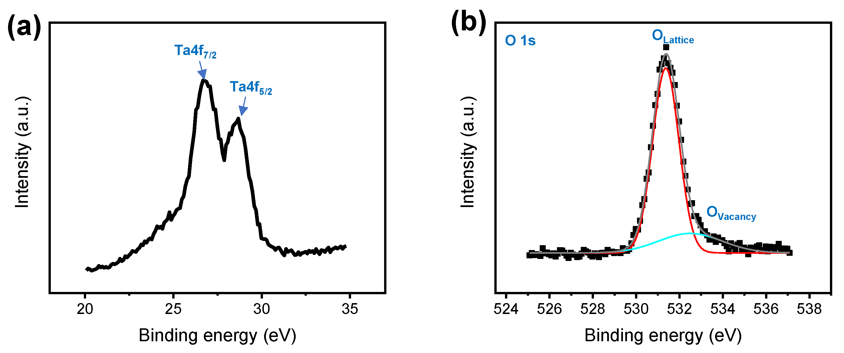
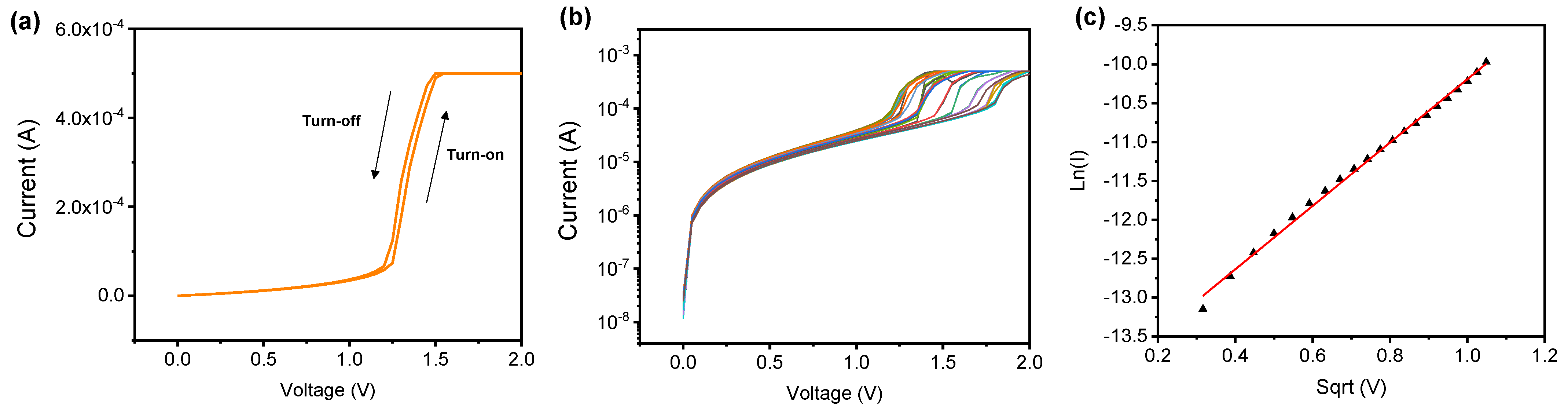
3. Results and Discussion

Figure 1a,b shows the XPS spectra of Ta 4f and O 1s of the DC sputtering deposited TaOx film, respectively. The XPS peaks for Ta 4f7/2 and Ta 4f5/2 of Ta-O bonds are located centered at around 26.72 eV and 28.65 eV, respectively (Figure 1a). On the other hand, the peak of Ta 4f for metallic Ta is not particularly detectable between 20 and 25 eV (Figure 1a). The main peak for O 1s of TaOx film is located at 531.38 eV, which is related to the oxygen lattice. On the other hand, a small peak is observed at the binding energy of 532.65 eV. This peak indicates the oxygen-deficient Ta-O bonds related to the oxygen vacancies.
Figure 2a shows the typical I–V curve (linear scale) for threshold switching of TiN/TaOx/ITO device. A dual I–V sweep is conducted to test the threshold switching. The current suddenly increases at turn-on voltage. The compliance current of 500 μA is essential to prevent the hard breakdown of the device. It is confirmed that the current decreased again at the turn-off voltage through the return voltage sweep. Even if only a forward sweep is performed without a return sweep, the threshold switching has a volatile characteristic, so the current has an off state again. In an actual RRAM memory cell, the set voltage should be greater than the turn-on voltage of the selector, and the reset current of the RRAM cell should be lower than the on-current of the selector. Figure 2b shows I–V curves (log scale) by an iterative sweep. There is a slight variation in turn-on voltage, which may adversely affect device operation when connected to RRAM devices. Therefore, more improvement is required through optimization of process conditions, etc. Next, we investigated the conduction mechanism of TiN/TaOx/ITO devices in the threshold switching mode. We performed various I–V fittings to check the conduction transport possible in the metal–insulator–metal (MIM) structure and confirmed that the I–V fitting for Schottky emission was the most accurate. Figure 2c shows the ln(I) versus sqrt (V) for Schottky emission. The result shows an exact curve of I–V fitting for Schottky emission in the regime before the turn-on voltage. That is until the device is turned on, electrons from the ITO electrode can jump over TaOx barrier layer by thermionic emission. A similar fitting result was reported in Pt/TaOx/Pt [29]. It is noted that the oxygen exchange could be dominated between TiN and TaOx layers for threshold switching when a positive bias is applied to the TiN electrode.
Next, the bipolar resistive switching with non-volatile property of TiN/TaOx/ITO devices is implemented. Figure 3a,b shows the repetitive I–V curves with compliance current (CC) and without CC, respectively. The indium ion could diffuse the dielectric and indium-based conduction filament could be formed when a negative bias is applied on TiN top electrode of the device. In the set process caused by indium diffusion from ITO electrode, the set voltage is very low regardless of the dielectric medium [30]. The reset process can be explained by an indium-based conducting filament or an increase in oxygen within TaOx layer. The current can be lowered at CC of 500 μA than the self-compliance current mode. This indicates the current overshoot can be minimized, and the current can be controllable by the CC. It is noted that negative-reset behavior that can make device failure does not occur at the large reset sweep voltage (~3 V) in Figure 3a. On the other hand, the current is limited by self-compliance during the set process (Figure 3b). The self-compliance could occur by the oxygen accumulation toward ITO electrode, which acts as series resistance. When the internal resistance of TaOx decreases during the set process, a relatively higher voltage could be applied to the oxygen-rich ITO side. The reset process is completed with a gradual increase in current. It is difficult to read the states at a positive bias because the set voltage is very low. However, it is possible to distinguish the states at the read voltage at a lower than reset voltage. It is noted that threshold switching does not occur well after bipolar resistive switching. This indicates that an indium ion could remain after the reset process. Figure 3c shows the log–log scale of LRS for Ohmic conduction in which the slope has 1. This indicates metallic filament composed of indium could be formed in the LRS. On the other hand, the HRS follows the Schottky emission, which is judged by the linear relationship of ln(I) versus sqrt (V) in Figure 3d. The Schottky barrier could exist after the rupture of indium filament in the HRS. Thus, the conduction occurs when electrons overcome the Schottky barrier formed at the interface between the TiN and TaOx layer with thermal energy. Figure 3e shows the retention test of LRS and HRS in which resistance values are extracted from reading voltage of −0.1 V. Two states have no degradation for 10,000 s, which means TiN/TaOx/ITO devices in the bipolar resistive switching mode has good data-storage ability.
Next, we demonstrated the pulse operation for threshold switching and set and reset processes in the bipolar resistive switching. Figure 4a shows the voltage and current as a function of time for the threshold switching. The read pulses with the voltage of 0.1 V before and after the pulse for threshold switching are applied to the device. Sufficient pulse width (1 ms) is applied to observe sufficient transient characteristics. After the pulse is applied, the current increases rapidly at about 300 μs, but the current is not maintained and decreases. Finally, the current is not detected by the read pulse, so we confirm the threshold switching with volatile memory property through this series of pulses. The set and reset processes for bipolar resistive switching are performed in a similar pulse application method. Figure 4a shows the transient characteristics for set process. It is observed that the current does not increase more than 300 μA due to self-compliance after the rapid increase in current. In the second read pulse, the current increase compared to the first, confirming that the set process goes well. It is noted that very low voltage (−0.4 V) can make the set process. Figure 2 exhibits a decrease in current by reset pulse with the amplitude of 0.9 V. The current is abruptly decreased in peak current is less than 500 μA.

4. Conclusions

In summary, we characterized both threshold switching and bipolar resistive switching from TiN/TaOx/ITO devices by controlling the bias polarity. The repetitive I–V curve for threshold switching was achieved with a positive bias on the TiN electrode. On the other hand, the set and reset processes for bipolar resistive switching were observed when a positive and negative bias was applied on the ITO electrode. The possible bipolar resistive switching mechanism can be explained by the formation and rupture of the indium conducting filament. We also demonstrated the pulse operation for the threshold and memory switching. The above result suggests two important switching possibilities simply by bias polarity for the selector and non-volatile memory applications.

Author Contributions

H.R. conducted the electrical measurements and wrote the manuscript; B.P. measured the electrical measurement partially; S.K. designed the experiment and supervised the study. All authors have read and agreed to the published version of the manuscript.

Funding

Korea Institute of Energy Technology Evaluation and Planning (KETEP) and the Ministry of Trade, Industry and Energy (MOTIE) of the Republic of Korea (no. 20194030202320).

Data Availability Statement

Not applicable.

Acknowledgments

Korea Institute of Energy Technology Evaluation and Planning (KETEP) and the Ministry of Trade, Industry and Energy (MOTIE) of the Republic of Korea (no. 20194030202320).

Conflicts of Interest

The authors declare no conflict of interest.

References

  1. Russo, U.; Ielemini, D.; Cagli, C.; Lacaita, A.L. Self-Accelerated Thermal Dissolution Model for Reset Programming in Unipolar Resistive-Switching Memory (RRAM) Devices. IEEE Trans. Electron. Dev. 2009, 56, 193–200. [Google Scholar] [CrossRef]
  2. Guo, M.Q.; Chen, Y.C.; Lin, C.Y.; Chang, Y.F.; Fowler, B.; Li, Q.Q.; Lee, J.; Zhao, Y.G. Unidirectional threshold resistive switching in Au/NiO/Nb:SrTiO3 devices. Appl. Phys. Lett. 2017, 110, 233504. [Google Scholar] [CrossRef]
  3. Kim, K.M.; Kim, G.H.; Song, S.J.; Seok, J.Y.; Lee, M.H.; Yoon, J.H.; Hwang, C.S. Electrically configurable electroforming and bipolar resistive switching in Pt/TiO2/Pt structures. Nanotechnology 2010, 21, 305203. [Google Scholar] [CrossRef]
  4. Lanza, M.; Wong, H.-S.P.; Pop, E.; Ielmini, D.; Strukov, D.; Regan, B.C.; Larcher, L.; Villena, M.A.; Yang, J.J.; Goux, L.; et al. Recommended Methods to Study Resistive Switching Devices. Adv. Electron. Mater. 2018, 5, 1800143. [Google Scholar] [CrossRef] [Green Version]
  5. Pan, F.; Gao, S.; Chen, C.; Song, C.; Zeng, F. Recent progress in resistive random access memories: Materials, switching mechanisms, and performance. Mater. Sci. Eng. R Rep. 2014, 83, 1–59. [Google Scholar] [CrossRef]
  6. Ryu, H.; Kim, S. Gradually Modified Conductance in the Self-Compliance Region of an Atomic-Layer-Deposited Pt/TiO2/HfAlOx/TiN RRAM Device. Metals 2021, 11, 1199. [Google Scholar] [CrossRef]
  7. Maikap, S.; Banergee, W. In Quest of Nonfilamentary Switching: A Synergistic Approach of Dual Nanostructure Engineering to Improve the Variability and Reliability of Resistive Random-Access-Memory Devices. Adv. Electron. Mater. 2020, 6, 2000209. [Google Scholar] [CrossRef]
  8. Choi, J.; Kim, S. Nonlinear Characteristics of Complementary Resistive Switching in HfAlOx-Based Memristor for High-Density Cross-Point Array Structure. Coatings 2020, 10, 765. [Google Scholar] [CrossRef]
  9. Mikhaylov, A.; Belov, A.; Korolev, D.; Antonov, I.; Kotomina, V.; Kotina, A.; Gryaznov, E.; Sharapov, A.; Koryazhkina, M.; Kryukov, R.; et al. Multilayer Metal-Oxide Memristive Device with Stabilized Resistive Switching. Adv. Mater. Technol. 2020, 5, 1900607. [Google Scholar] [CrossRef]
  10. Ismail, M.; Kim, S. Negative differential resistance effect and dual resistive switching properties in a transparent Ce-based devices with opposite forming polarity. Appl. Sur. Sci. 2020, 530, 147284. [Google Scholar] [CrossRef]
  11. Peng, C.S.; Chang, W.Y.; Lin, M.H.; Chen, W.S.; Chen, F.; Tsai, M.J. Polarity Reversion of the Operation Mode of HfO2-Based Resistive Random Access Memory Devices by Inserting Hf Metal Layer. J. Nanosci. Nanotechnol. 2013, 13, 1733–1737. [Google Scholar] [CrossRef] [PubMed] [Green Version]
  12. Ryu, H.; Kim, S. Gradually Tunable Conductance in TiO2/Al2O3 Bilayer Resistors for Synaptic Device. Metals 2021, 11, 440. [Google Scholar] [CrossRef]
  13. Cho, H.; Kim, S. Emulation of Biological Synapse Characteristics from Cu/AlN/TiN Conductive Bridge Random Access Memory. Nanomaterials 2020, 10, 1709. [Google Scholar] [CrossRef] [PubMed]
  14. Choi, J.; Kim, S. Coexistence of Long-Term Memory and Short-Term Memory in an SiN x-Based Memristor. Phys. Status Solidi RRL 2020, 14, 2000357. [Google Scholar] [CrossRef]
  15. Park, M.; Kang, M.; Kim, S. Pulse frequency dependent synaptic characteristics in Ta/SiN/Si Memristor Device for Neuromorphic System. J. Alloys Compd. 2021, 882, 160760. [Google Scholar] [CrossRef]
  16. Lee, M.J.; Lee, C.B.; Lee, D.; Lee, S.R.; Chang, M.; Hur, J.H.; Kim, Y.B.; Kim, C.J.; Seo, D.H.; Seo, S.; et al. A fast, high-endurance and scalable non-volatile memory device made from asymmetric Ta2O5−x/TaO2−x bilayer structures. Nat. Mater. 2011, 10, 625–630. [Google Scholar] [CrossRef]
  17. Ryu, H.; Kim, S. Irregular Resistive Switching Behaviors of Al2O3 -Based Resistor with Cu Electrode. Metals 2021, 11, 653. [Google Scholar] [CrossRef]
  18. Yang, J.; Ryu, H.; Kim, S. Resistive and synaptic properties modulation by electroforming polarity in CMOS-compatible Cu/HfO2/Si device. Chaos Solitons Fractals 2021, 145, 110783. [Google Scholar] [CrossRef]
  19. Park, J.; Ryu, H.; Kim, S. Nonideal resistive and synaptic characteristics in Ag/ZnO/TiN device for neuromorphic system. Sci. Rep. 2021, 11, 16601. [Google Scholar] [CrossRef]
  20. Chandrasekaran, S.; Simanjuntak, F.M.; Saminathan, S.; Panda, D.; Tseng, T.Y. Improving linearity by introducing Al in HfO2 as a memristor synapse device. Nanotechnology 2019, 30, 445205. [Google Scholar] [CrossRef]
  21. Ryu, H.; Choi, J.; Kim, S. Voltage Amplitude-Controlled Synaptic Plasticity from Complementary Resistive Switching in Alloying HfOx with AlOx-Based RRAM. Metals 2020, 10, 1410. [Google Scholar] [CrossRef]
  22. Ryu, H.; Kim, S. Pseudo-Interface Switching of a Two-Terminal TaOx/HfO2 Synaptic Device for Neuromorphic Applications. Nanomaterials 2020, 10, 1550. [Google Scholar] [CrossRef] [PubMed]
  23. Kim, T.H.; Nili, H.; Kim, M.H.; Min, K.K.; Park, B.G.; Kim, H. Reset-voltage-dependent precise tuning operation of TiOx/Al2O3 memristive crossbar array. Appl. Phys. Lett. 2020, 117, 152103. [Google Scholar] [CrossRef]
  24. Govoreanu, B.; Adelmann, C.; Redolfi, A.; Zhang, L.; Clima, S.; Jurczak, M. High-Performance Metal-Insulator-Metal Tunnel Diode Selectors. IEEE Electron. Dev. Lett. 2013, 35, 63–65. [Google Scholar] [CrossRef]
  25. Fong, S.W.; Neumann, C.M.; Wong, H.S.P. Phase-Change Memory—Towards a Storage-Class Memory. IEEE Trans. Electron. Mater. 2017, 64, 4374–4385. [Google Scholar] [CrossRef]
  26. Li, S.; Pam, M.E.; Li, Y.; Chen, L.; Chien, Y.C.; Fong, X.; Chi, D.; Ang, K.W. Wafer-Scale 2D Hafnium Diselenide Based Memristor Crossbar Array for Energy-Efficient Neural Network Hardware. Adv. Mater. 2021, 2103376. [Google Scholar] [CrossRef] [PubMed]
  27. Lee, Y.; Mahata, C.; Kang, M.; Kim, S. Short-term and long-term synaptic plasticity in Ag/HfO2/SiO2/Si stack by controlling conducting filament strength. Appl. Sur. Sci. 2021, 565, 150563. [Google Scholar] [CrossRef]
  28. Lee, K.J.; Chang, Y.C.; Lee, C.J.; Wang, L.W.; Wang, Y.H. Bipolar Resistive Switching Characteristics in Flexible Pt/MZT/Al Memory and Ni/NbO2/Ni Selector Structure. IEEE J. Electron. Dev. Soc. 2018, 6, 518–524. [Google Scholar] [CrossRef]
  29. Huang, Y.; Huang, R.; Cai, Y.; Wu, H.; Yue, P.; Zhang, Y.; Chen, C.; Wang, Y. A TaOx based threshold switching selector for the RRAM crossbar array memory. In Proceedings of the 12th Annual Non-Volatile Memory Technology Symposium Proceedings, Singapore, 31 October–2 November 2012. [Google Scholar] [CrossRef]
  30. Lin, Z.H.; Wang, Y.H. Observation of indium ion migration-induced resistive switching in Al/Mg0.5Ca0.5TiO3/ITO. Appl. Phys. Lett. 2016, 109, 053507. [Google Scholar] [CrossRef]
Figure 1. XPS spectra of TaOx film (a) Ta 4f and (b) O 1s.
Metals 11 01531 g001
Figure 2. (a) Typical threshold switching and (b) repetitive curve of TiN/TaOx/ITO devices, (c) Fitting plot for ln(I) versus sqrt (V) of threshold I–V curve.
Metals 11 01531 g002
Figure 3. I–V curve of TiN/TaOx/ITO devices when set and reset processes at a negative bias and a positive bias, respectively. (a) Low current switching operation with CC and (b) high current switching with self-compliance. (c) Log–log scale in LRS and (d) ln(I) versus sqrt (V) fitting plot in the HRS. (e) Retention time of LRS and HRS.
Metals 11 01531 g003
Figure 4. Pulse transient characteristics for (a) volatile switching. (b) Set process and (c) reset process for memory resistive switching.
Metals 11 01531 g004
Publisher’s Note: MDPI stays neutral with regard to jurisdictional claims in published maps and institutional affiliations.

