Review

Recent Progress in Transient Liquid Phase and Wire Bonding Technologies for Power Electronics

1
Department of Materials Science and Engineering, University of Seoul, 163 Seoulsiripdae-ro, Dongdaemun-gu, Seoul 02504, Korea
2
Department of Energy Systems Research and Department of Materials Science and Engineering, Ajou University, Suwon 16499, Korea
*
Author to whom correspondence should be addressed.
Metals 2020, 10(7), 934; https://doi.org/10.3390/met10070934
Submission received: 8 June 2020 / Revised: 5 July 2020 / Accepted: 7 July 2020 / Published: 11 July 2020

Abstract

:
Transient liquid phase (TLP) bonding is a novel bonding process for the joining of metallic and ceramic materials using an interlayer. TLP bonding is particularly crucial for the joining of the semiconductor chips with expensive die-attached materials during low-temperature sintering. Moreover, the transient TLP bonding occurs at a lower temperature, is cost-effective, and causes less joint porosity. Wire bonding is also a common process to interconnect between the power module package to direct bonded copper (DBC). In this context, we propose to review the challenges and advances in TLP and ultrasonic wire bonding technology using Sn-based solders for power electronics packaging.

1. Introduction

Due to rapid progress in power electronics and packaging devices, there is a strong demand for better joining materials and processes. However, conventional silicon power module devices are now being replaced with high power ceramic modules made of SiC or AlN packages, which have better thermal stability at higher temperatures [1]. Thinner die packages combined with high speed and density require new packaging materials to support the device applications [2]. The power module is an essential component of power electronics for performing power conversion and supply or switching supply while maintaining stability and efficiency [3]. All power modules are used in inverter or converter circuits of on-board devices, but their types vary depending on the circuit configuration and the specifications of the modules [4]. The popular insulated gate bipolar transistor (IGBT) power module package used for power conversion is shown in Figure 1. It consists of several components, e.g., heat sink, base plate, and direct bonded copper (DBC) substrate with attachment material [3,4,5]. The top side of the module has wire-bonded elements connected to an IGBT diode and the external lead frames. The IGBT is bonded to the DBC with die attachments, as shown in Figure 1. The IGBT module is generally encapsulated with multiple diodes, metal-oxide field-effect transistors (MOSFETs), and intelligent power modules (IPMs) for the surface protection of wire bonds from the external atmosphere. These power semiconductors are generally bonded with a die attach material or soldered to the DBC substrate for electrical and thermal contact and insulation when necessary. In modern versions of power modules, the IPM mounts a dedicated circuit for drawing maximum power from the IGBT and minimizing electromagnetic shielding effect for the protection of the entire device.
Recently, the development of high-reliability, high-efficiency power devices suitable for eco-friendly applications such as electric vehicles or hybrid vehicles has attracted much attention. Likewise, interest in high-reliability power modules is also growing among electronic manufacturers. The enhancement in the reliability of the power modules is directly related to the highly reliable wire bonding technology and joining process for the die attachment over the semiconductor insulated-gate bipolar transistor (IGBT) [5,6]. The primary bonding methods for power modules include Ag and/or Cu powder sintering [7], Sn-based transient liquid phase (TLP) bonding [8,9], etc., while Al wire, Al-0.5Cu wire, and Al-0.005Ni wire are used for wire bonding. Various Al wires are used in the form of Al ribbon, Cu-Al clad ribbon, and Cu wires [10,11].
It is also to be noted that in modern power module circuits and assemblies, various metallic conductors are also needed to be joined to the ceramic dies and circuits [12,13,14]. Various authors have suggested the use of active metal soldering and/or brazing or low-temperature Zn-based soldering [15,16,17,18].
Various Zn-based solders, such as Zn6Al, Zn6Al1Ga, Zn3Al3Mg, and Zn4Al3Ga3Mg, have been used as lead-free alternatives by Rettenmayr et al. [19]. However, such types of solders are associated with high brittleness due to the temperature dependence of Ga solubility in Zn as well as the formation of Ga compounds rich in Al and Zn. This brittleness of solder can be avoided by decreasing the solubility at higher temperatures.
Shimizu et al. [20] used various additive elements (Sn, In, and Ge) to the Zn4Al3Mg and Zn6Al5Ge alloys to replace Pb-5Sn solder for die-attached applications [20]. Although a good die-attaching property was observed at higher temperatures, the addition of Sn, In, and Ga deteriorated the workability and stress relaxation ability of this alloy. In another study, Cheng et al. [21] showed that the addition of Sn to Zn4Mg3Al alloys caused a reduction of uniaxial tensile strength with increasing temperature. The elongation ratio was poor at 200 °C but improve at 100 °C compared to room temperature.
Ceramics such as sapphire were bonded directly by ultrasound-assisted soldering by Sn10Zn2Al solder by Cui et al. [22]. The bond formation was noticed by the presence of a nanocrystalline alumina layer on the Sn-Zn-Al/sapphire interface while reflowing at 230 °C.
Active metal brazing has been used regularly to braze ceramics to metals in various applications. Pioneering work on ceramic metal bonding was done by Jung et al. [23]. Active brazing generally includes Ag-Cu eutectic with the addition of Ti or Nb, which promotes wetting [23,24]. Additionally, recent high entropy alloys have also been tested for their joining applications, and experiments are underway by several researchers [25]. High entropy alloys have shown impressive properties due to their high mixing entropy, which favors the formation of solid solution phases compared to intermetallic compounds. However, these alloys are still at the beginning stage in the field of microjoining [26].
Although there are various active reports on power modules, there is not yet enough literature summarized in terms of the joining of power module devices. Therefore, in this paper, the authors intend to review the details of recent research trends in TLP bonding and wire bonding, which are one of the important elements for power module packaging. We choose to focus on cheaper Sn-based solders for TLP bonding compared to expensive Ag-based die-attached materials. In this manuscript, Section 1 describes the introduction to the power modules. Section 2 describes various joining processes of power modules and semiconductor devices. Section 3 deals with the comparison of TLP bonding with solid-state diffusion bonding and brazing. Section 4 and Section 5 deal with the various factors and materials used for TLP bonding, while Section 6 is devoted to ultrasonic wire bonding. In the wire bonding section, we discuss wire and wedge bonding and the recrystallization process during ultrasonic bonding, followed by reliability studies in Section 8. The conclusions are given in Section 9. Finally, future directions and outlook are given in Section 10.

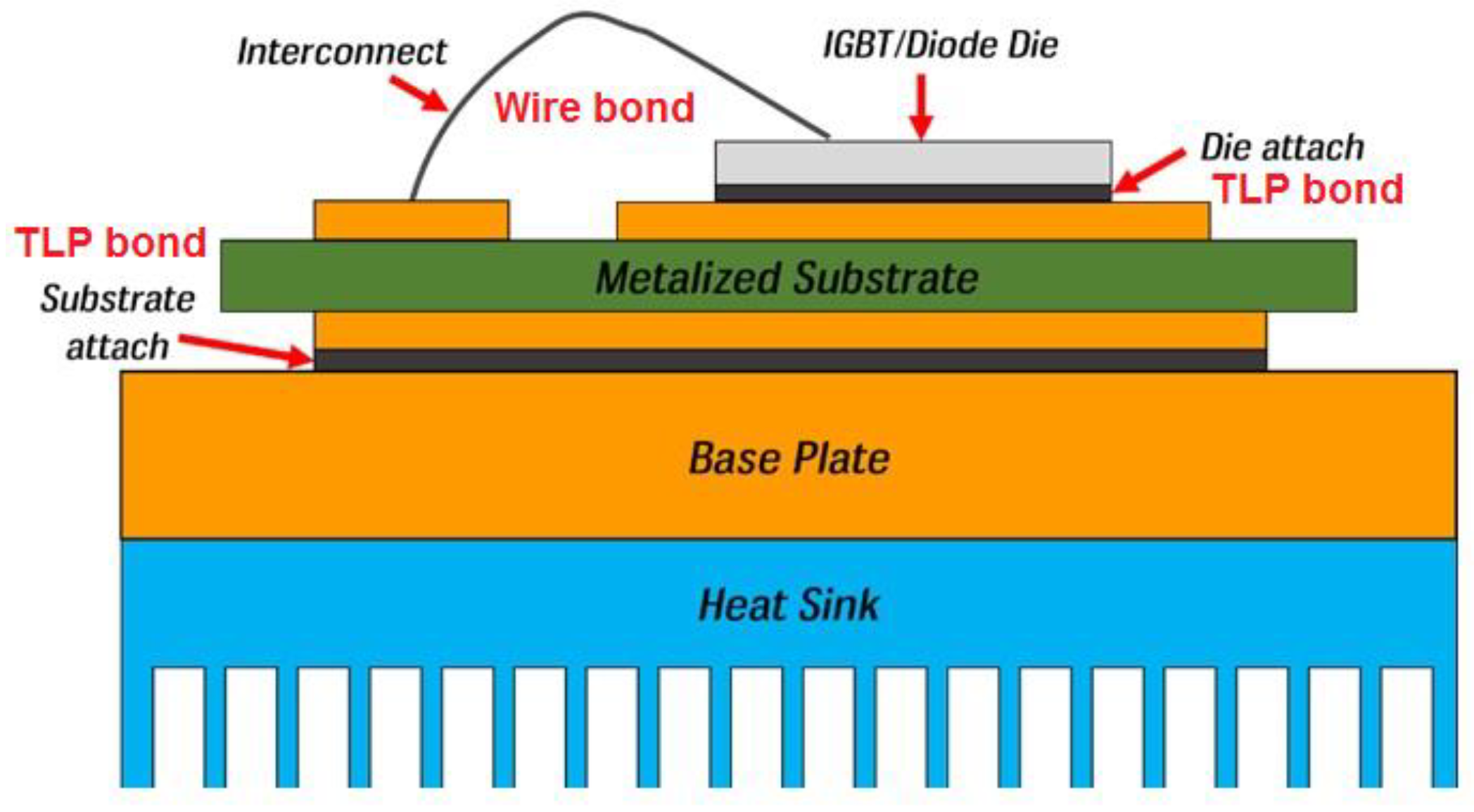
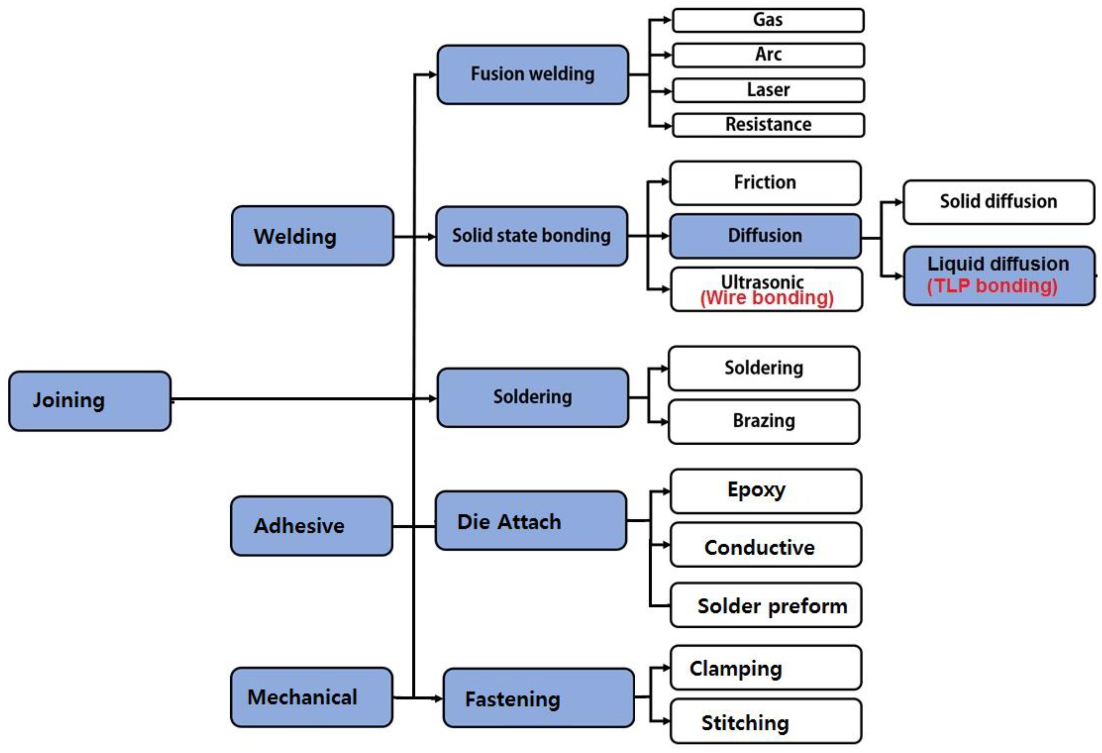
2. Joining Process Used for Power Modules

There are many different types of joining processes. According to the established research, classification of joining processes can be summarized as shown in Figure 2 [11,27]. Different joining processes are divided into fusion welding, solid-state bonding, and soldering. In fusion welding, both the parent metal and filler melt into the weld joint. In solid-state bonding, however, both base metal and insert metal do not melt in the process [28]. Moreover, in brazing, only the filler metal melts but the base metal remains as a solid.
In the solid-state joining method, the base material is joined without melting, while in brazing and soldering, the base material is not melted but is joined by melting the filler. The solder filler operates below 450 °C, while brazing is performed above 450 °C [28]. The fusion welding methods, including the well-known arc welding, flame welding, laser welding, and electron beam welding, operate at even much higher temperatures. Diffusion bonding, ultrasonic bonding, and friction bonding are typical examples of the solid-state bonding method [11,27,28]. Among the solid-state bonding methods, the diffusion bonding method is one of the basic bonding methods, where a mutual diffusion occurs in the solid-state between atoms across both sides to be joined by applying pressure and/or high bonding temperature close to the bonding surface [28,29]. In diffusion bonding, there is no formation of a bonding layer, which improves mechanical reliability as the physicochemical properties of the parent metal remain the same. Furthermore, the diffusion bonding can be easily applied to the bonding of alloys or dissimilar metals that are difficult to melt/weld [29]. However, there is a possibility that the material to be joined is deformed by pressure applied to the material to be joined at a high temperature during bonding. There is also a disadvantage that a flat bonding surface is required to reduce defects such as pores in the bonding interface; furthermore, the bonding time is longer.

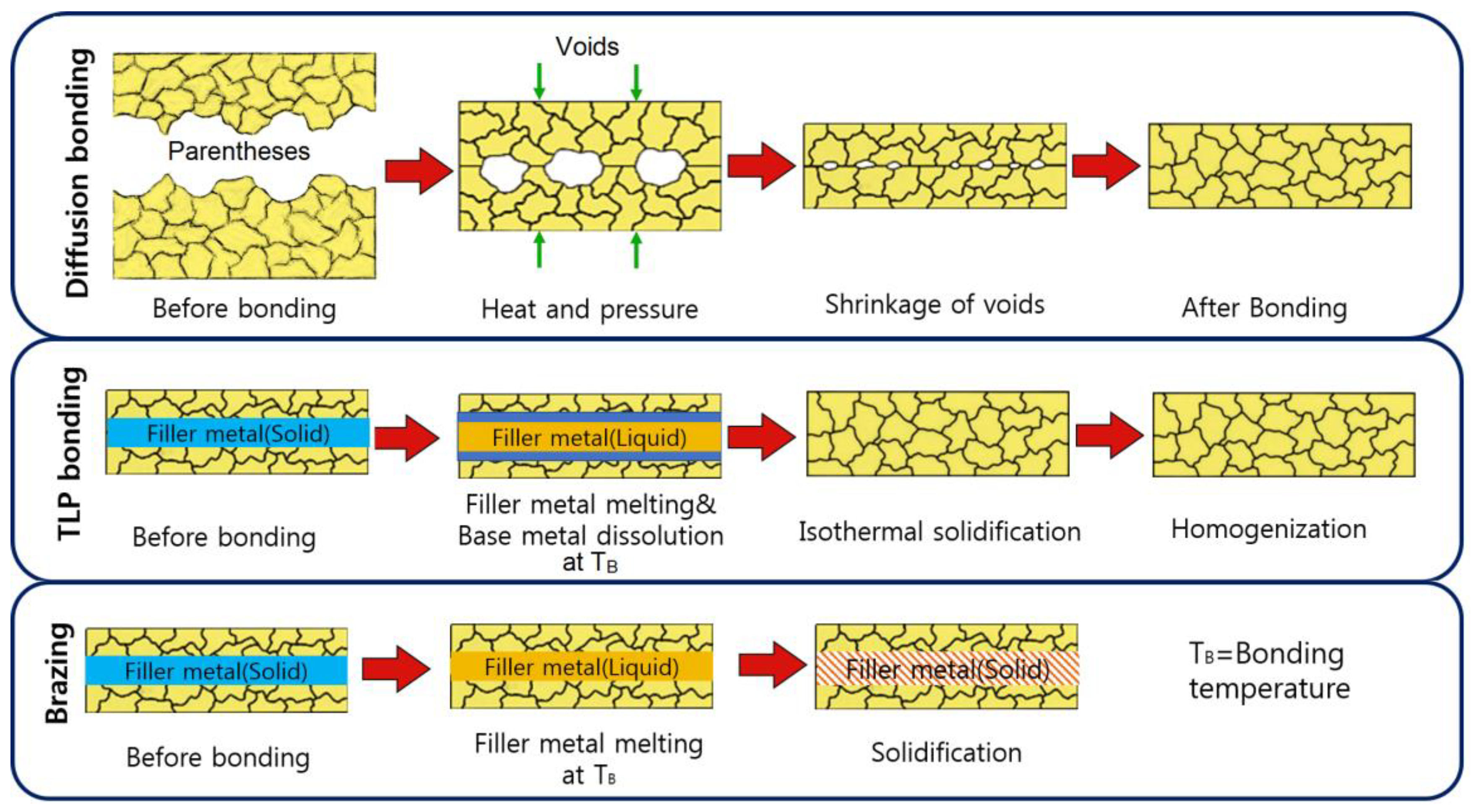
3. TLP Bonding Compared to Solid-State Diffusion Bonding and Brazing

A method designed to improve the shortcomings of solid phase diffusion bonding is a liquid phase diffusion (TLP) bonding method. In modern power electronics devices, TLP bonding has become a potential candidate for joining DBC to semiconductor chips. TLP bonding combines the merits of brazing and solid-state diffusion bonding and is also known as diffusion brazing [29,30]. It is similar to brazing because the bonding material is melted but the base material is not melted (only some interface parts are melted) and is similar to the solid-phase diffusion bonding method as a method of solidifying bonding by diffusion. The TLP bonding method was studied and proposed by Hoppin [31] and Duvall [32] in the early 1970s. During TLP bonding, the liquid phase is transiently present at the bonding surface. Figure 3 compares solid-state diffusion bonding, brazing, and TLP bonding processes.
We can see that the solid-state diffusion bonding method proceeds in various steps. First, the parentheses are formed across the joint interface. After applying pressure, these parentheses come to closure, and pores are formed, and deform plastically and shrinkage of voids occurs before final bonding [28]. Brazing involves the melting and heating of the filler material across the interface followed by solidification and joining. In contrast, TLP bonding involves the melting and heating of the bonding materials followed by the transient liquid phase and its isothermal solidification and homogenization before complete bonding occurs [29,30].
In principle, the TLP bonding method has a unique solidification characteristic that solidifies at an isotherm due to a decrease in the concentration of the low melting point element in the bonding material [31,32]. The melting point lowering element contained in the bonding material diffuses into the bonding material [33]. Various bonding couples have been used for TLP bonding including steel and superalloys (Rene 80), such as Rene 80/B [34], stainless steel [35], Ni/B/Ni [36], and Rene80/B/Rene80 [37]. All these reports showed an isothermal solidification characteristic in which the liquid is converted to a solid at the same temperature; high-temperature strength and high reliability are obtained because the joint does not re-melt even when heated to the bonding temperature after solidification [38,39].

4. Factors Affecting TLP Bonding

The various factors affecting TLP bonding are time, bonding temperature, and alloying elements in the Sn-based solder. Among these factors, the bonding temperature is usually limited by the thermal stability of the substrates [40,41]. A minimum isothermal solidification time can be met at a fixed bonding temperature. Therefore, the major influence comes from bonding time at a particular temperature. We will discuss these factors in the following subsections.

4.1. Alloying Elements in Sn-Based Solder

Traditionally, TLP bonding involves the addition of interstitials such as boron, carbon, or phosphorus for depression of melting point during the joining of Cu alloys [29,33]. This is crucial to bonding properties, because the meting point of the filler increases during isothermal solidification. However, the TLP bonding of the microelectronic devices relies on the low-temperature Pb-free Sn-Pb solders due to recent Pb-free and environmental regulations. Furthermore, power modules can be exposed to a higher temperature due to the continuous thinning of die size to improve high density and integration [4,6,8]. Therefore, the reliability of the Pb-free Sn-based solders becomes important to meet this trend.
The TLP bonding method based on Sn-based alloy or solder mainly used in the electronics industry manly uses various Sn-based solders such as Sn-Cu, Sn-Ni, or Sn-Ag as a bonding material, and if necessary, other metal powders such as Cu can be added to it. However, the formation of brittle intermetallic compounds (IMCs) during joining suppresses the concept of isothermal solidification due to the decrease in concentration caused by the diffusion of low melting point elements toward the base material [29,33]. This is because Sn and Cu, Ni, Ag, and the like in the bonding material react with each other to form the IMCs in the entire joint, thereby increasing the high-temperature strength of the joint [29].
Recently, the boundaries of the TLP process have been expanded to the joining of electronic parts. Among them, the TLP bonding applied to the Sn-based solder has become popular in recent investigations. Unlike the conventional TLP bonding process, Sn-based solder does not contain interstitial elements as melting point depressants. Instead, Sn contains the substitutional elements Ag, Cu, or Ni as melting point depressants, which further impart strength to the joint by precipitation hardening caused by Ag3Sn, Cu6Sn5, and Ni3Sn4 IMCs [29,30]. A survey of various elemental additions in Sn-based solder used for TLP bonding is presented in Table 1.
The melting point inhibitors such as Ag, Cu, or Ni in Sn do not have high diffusivity in solid base Cu, and it takes a longer time for isothermal solidification. The major Sn-based solder systems include Sn-3.5Ag, Sn-0.7Cu, and Sn-3.0Ag-0.5Cu. To change the molten solder to a solidified IMC such as Cu6Sn or Cu3Sn, even though some Sn is diffused as a solid, a sufficient amount of Cu must be present in the molten solder [55,56]. This leads to a longer bonding time and also reduces joint stability. On the other hand, non-metallic IMCs Cu6Sn5, Cu3Sn, Ag3Sn, and Ni3Sn4 have higher melting points than the Sn-based solder, and the thermal resistance of the joint increases compared to ordinary soldering [57,58,59]. Hosseinzaei et al. [62] used a Cu-Sn solder system, and Sn-3.5Ag was employed by Choudhury et al. [63].

4.2. Bonding Time

The essential drawback of the TLP bonding is long bonding time, which comes mostly from isothermal solidification of solder and completion of IMC transformation during bonding. Various methods have been attempted to reduce TLP bonding time. Figure 4 shows the effect of bonding time at a fixed temperature of 485 °C for 10 and 30 min by using Cu coatings for the Cu-Mg system [10].
According to Hosseinzaei et al. [62], for the Cu-Sn couple, all of Sn was consumed and transformed to Cu6Sn5 and Cu3Sn after 60 min, while after 120 min, in all joints the Cu6Sn5 phase had completely disappeared and transformed to Cu3Sn at the expense of the Cu6Sn5 + Cu until all of the Cu6Sn5 disappeared.
Sohn et al. [64] investigated the behavior of the liquid layer in TLP bonding with time. They calculated the width of the liquid transient layer after the isothermal solidification and proposed the bonding mechanism. Further research reported that the bonding time is closely related to the width of the liquid layer at the bonding joint of liquid metal [35,65]. According to previous results, the width of the liquid layer at time t (Wt) follows the relation [33]
W t = W M k D ( t t M )
where k is a constant, D is the diffusivity of filler (solder) at the bonding temperature, t M is the time to reach the maximum width of the liquid layer W M , and W M is proportional to the initial thickness of the solder layer W 0 .
The isothermal solidification time t f can be obtained when the joint is isothermally solidified: W M → zero, and t t f . Therefore, rearranging Equation (1), we can find t f as follows [33]:
t f = A W 2 M D + t M
where A is a constant. To understand the mechanism of TLP bonding, Shao et al. [66] calculated the average radius of the Ag3Sn grains formed in TLP soldering of Ag/Sn according to the following equation:
R ( t ) = ( K g b t ) 1 2
where R(t) is the average radius of the Ag3Sn grains at a given time t. The constant Kgb is the growth rate constant given by
K g b = D g b σ V m δ g b R T
D g b and σ denote grain boundary diffusivity and energy, respectively, V m is the molar volume of Ag3Sn, δ g b is grain boundary thickness, R is the universal gas constant, and T is the temperature in Kelvin. They proposed that Ag3Sn growth kinetics follows a parabolic relationship with soldering time t during TLP bonding.
Minimization of TLP bonding time is an important issue in TLP bonding to satisfy the large scale productivity in power industries. The time duration can be effectively cut off by avoiding the isothermal solidification time; however, isothermal solidification benefits the joint by the formation of IMCs. Otherwise, there may be some traces of Sn or Sn-X (X = Cu or Ag) eutectic solder remains in the joint which has a lower melting point than IMCs and can damage the entire power module assembly. Most of the power module usually needs thermal resistance over 300 °C, while the remained Sn solder melts near 230 °C. Recently, to reduce bonding time in the TLP process, quite a small amount of solder, such as 5 μm in thickness, has been suggested. Most of the research activities are devoted to the use of various melting point reducing agents in the liquid metal for the isothermal solidification in TLP bonding [67]. Most widely used meting point depressants are pure C, B, or phosphorus as an interstitial element to reduce the isothermal solidification time [35,64,68]. Notable reduction in TLP bonding time has been obtained, to yield a very short 10 to 15 min, which covers the entire isothermal solidification and composition homogenization duration [35,52,53,54,55,56,57,58,59,60,61,62,63,64]. More recently, the use of Sn coated Cu powders or Sn-Cu coated carbon nanotubes has been documented in past research. Rajendran et al. [8] investigated the TLP bonding of Cu platelets using Sn coated Cu multiwalled CNT composite solder paste with RMA (rosin mildly activated) type flux. The thickness of the solder paste printed on the Cu platelet was 150 μm. The joint transformed into Cu3Sn IMC completely after 8 min bonding at 260 °C, which is considerably shorter than that of other TLP bonding using normal solder [8].

4.3. Shear Strength

Other researchers have also analyzed the effect of TLP bonding time on mechanical and joint shear strengths. The microhardness of the Cu6Sn5 is higher than that of the Cu3Sn, e.g., 894 and 689 HV, respectively. The shear strength after bonding at 300 °C for 15 min (Sn + Cu6Sn5 + Cu3Sn phases), 60 min (Cu6Sn5 + Cu3Sn phases), and 120 min (Cu3Sn phase) were 11.7, 9.5, and 5.4 MPa, respectively. Reduced joint strength was correlated to the brittleness of IMCs and void production along the joint after Cu3Sn covered the whole joint [68]. Moreover, the joint strength depends upon the volume fraction of IMCs. The shear strength was increased at a smaller volume fraction of IMCs while the failure strain decreased steadily up to a higher volume fraction of IMCs [68].

5. TLP Bonding with Different Filler Shapes

The shape and size of the filler powder affect the TLP bonding appreciably. For example, with a bigger powder particle size, paste printing becomes difficult with large IMCs. On the contrary, smaller particles will tend to segregate during TLP bonding and may cause premature failure of the joint. Therefore, the selection of filler shapes and structure is a great demand in modern TLP processes. In this section, we review various types of TLP bonding processes with different fillers.

5.1. Foil Type Interlayers

Several researchers in the past [67,68] have used Sn foil as an interlayer to join Cu-Sn, Ni-Sn, or Sn-Ag via TLP bonding. Chu et al. [69] studied and compared two sandwiched solder systems (Cu/Sn/Cu and Ni/Sn/Ni) for low-temperature wafer bonding at 255 °C for 5 min. To understand the mechanical reliability of the soldered joint, the thickness ratio of Cu/Sn (Ni/Sn) was controlled. They found that the presence of Ni deteriorated joint reliability. The Cu/Sn/Cu joint was found to be stronger and showed an intragranular fracture of Cu6Sn5 particles, while the Ni/Sn/Ni joint exhibited intergranular fracture through the Ni3Sn4 grain boundary and the Ni3Sn4/Ni3Sn2 interphase boundary.
Shao et al. [70] studied TLP through capillary action for high-density power device packaging using hybrid solder consisting of a layer of Cu powders and Sn foils. They reported high heat-resistant joints characteristic of Cu-Sn IMCs and dispersed Cu particles, even at a temperature of 250 °C within 20 min. Brincker et al. [71] studied the reliability of Cu/Sn/Cu through low-temperature TLP bonding at 255 °C for 5 min at 25 MPa. The microstructural and optical microscopy studies of the samples revealed good homogeneity with a significant reduction in the pore density at the interface. Zhao et al. [72] employed ultrasonic-assisted TLP bonding for Cu-Sn couples in a very short time of 8 min at 280 °C. In their study, Cu6Sn5 and Cu3Sn IMCs showed a new non-interface growth pattern in the liquid melt interlayer with a combination of intergranular and intergranular destruction during shear tests. Other reports include the use of Au-Sn foils for Ni-Cu alloys to enhance the mechanical reliability at high temperatures They explained that a ductile Au-Cu (ordered AuCu or disordered (Au,Cu)) layer can release local stress developed across the joint and improve the mechanical reliability. The shear strength of the Au-Sn/Ni-40Cu joint reached from 87 to 97 MPa after exposure from 400 to 450 °C for 24 h, respectively. Elmer et al. [73] also used Au-Sn foil for high-temperature reliability of Au-20Sn eutectic solder alloy between 125 and 200 °C. Similarly, Zhu et al. [74] investigated Au-20Sn solder for the assembly of e IGBT chips and DBC substrate for power applications. They suggested that TLP bonding at 300 °C for the 60 s followed by aging at 240 °C for 100 h is an excellent method to realize low-temperature bonding. Further, Peng et al. [75] also studied the effect of Cu content on the interface and shear behavior of Ni-xCu substrate using Au-29 at.% Sn solder foil at 350 °C. They suggested that the maximum content of Cu should be 40 at.% for maximum shear strength of 62 MPa and remain above 52 MPa during long soldering times. However, TLP bonding with metal interlayers is a traditional way of joining two surfaces and cannot be satisfactorily applied to the microelectronic packages used for advanced printing processes with higher-level integrations [76,77]. Researchers are moving to other filler shapes for more flexibility in power device packaging applications [78,79].

5.2. Powder and Paste Fillers

In recent power applications, powder type fillers have been used extensively due to the flexibility in printing technology and complex geometry of advanced packaging devices. Solder powder, micron-sized balls, and paste have been used for normal surface mount soldering in electronics [79,80,81]. Fujino et al. [81] mixed Ag-(30–50 wt.%)Sn powders, and preheated at 125 °C for 10 min and held at 260 °C for 1 min which is a quite short time to join Si-die with DBC. Similarly, a mixture of Ag and (Sn-0.3Ag-0.7Cu) solder paste has been used by Bao et al. [82]. The formation of Ag3Sn in Ag bearing solder pastes provides better thermal conductivity and fracture toughness as compared to Cu-Sn and Ni-Sn systems.
In such a TLP process, various researchers have used low melting Sn-based solder powder mixed with higher melting point elements like Cu, Ni, or Ag powder to produce IMCs in the entire joint [82,83]. As a result, the melting temperature of the bonded zone exceeds the bonding temperature in a short time by forming various IMCs, which improve the high-temperature strength [84]. Lang et al. [85] studied the ultrasonic-assisted bonding of Cu-Sn and obtained a Cu-Cu3Sn-Cu structure with a shear strength of 275 MPa at 260 °C.
Sun et al. [86] investigated the effect of grain orientation of IMCs in the joint to control the formation of voids. They found that the growth of Cu3Sn is controlled by grain boundary diffusion. The preferred orientations of Cu6Sn5 and Cu3Sn grains were (001) and (100), respectively. To solve the problem of voiding, Mokhtari et al. [51] suggested the use of Cu particles inside Sn-Bi solder for TLP bonding, which also contributes to the improved shear strength of the solder joint.
Liu et al. [87] used formic acid activation of the Sn-coated Cu particles for low-temperature die-attached applications. The joint shear strength was improved due to the formation of Cu3Sn IMCs with dispersions of Cu particles. In another study, they used Sn-coated micron-sized Cu particles as die-attached materials for Cu-Cu TLP bonding at 300 °C for 30 s. The shear strength was 25 MPa, which is equivalent to that of conventional Pb-5Sn solder. The shear strength of the joint was almost stable even after isothermal aging at 300 °C for 200 h [56].
Hu et al. [57] also reported low-temperature bonding using Cu-Sn core-shell particles as new die-attached material. They reported that reflow soldering at 250 °C for 40 min resulted in the transformation of outer Cu6Sn5 into Cu3Sn. The shear strengths of the resulting bond lines after reflow soldering at 250 °C for 8 and 40 min were 29.35 and 18.78 MPa at 400–500 °C, respectively. The results showed that a smaller reflow time induced the formation of Cu6Sn5 and Cu3Sn, while a longer reflow time transformed Cu6Sn5 into Cu3Sn entirely after the TLP process was finished, which improved the high-temperature strength of the bond lines, as shown in Figure 5.
To clarify the joint reliability at higher temperature die-attached applications, the evolution of the transient liquid-phase sintered (TLPS) Cu-Sn skeleton during thermal aging was reported by Tatsumi et al. [88]. Thermal aging at 150–200 °C for 1000 h caused the transformation of Cu6Sn5 IMCs fully into Cu3Sn. Yang et al. [89] reported microstructure and mechanical performance using In-Sn-20Cu composite fillers for TLP soldering of Cu plates. The TLP solder joint produced Cu3(In, Sn) and Cu6(In, Sn)5 after isothermal solidification. The shear strength of Cu/In-Sn-20Cu/Cu joint was 26.54 MPa at 15 min. In all these studies, either a longer duration of bonding time was needed or special thermal aging was required to improve the interface strength. Recently, there have been many reports of using an advanced composite approach for enhancing the TLP bonding strength.

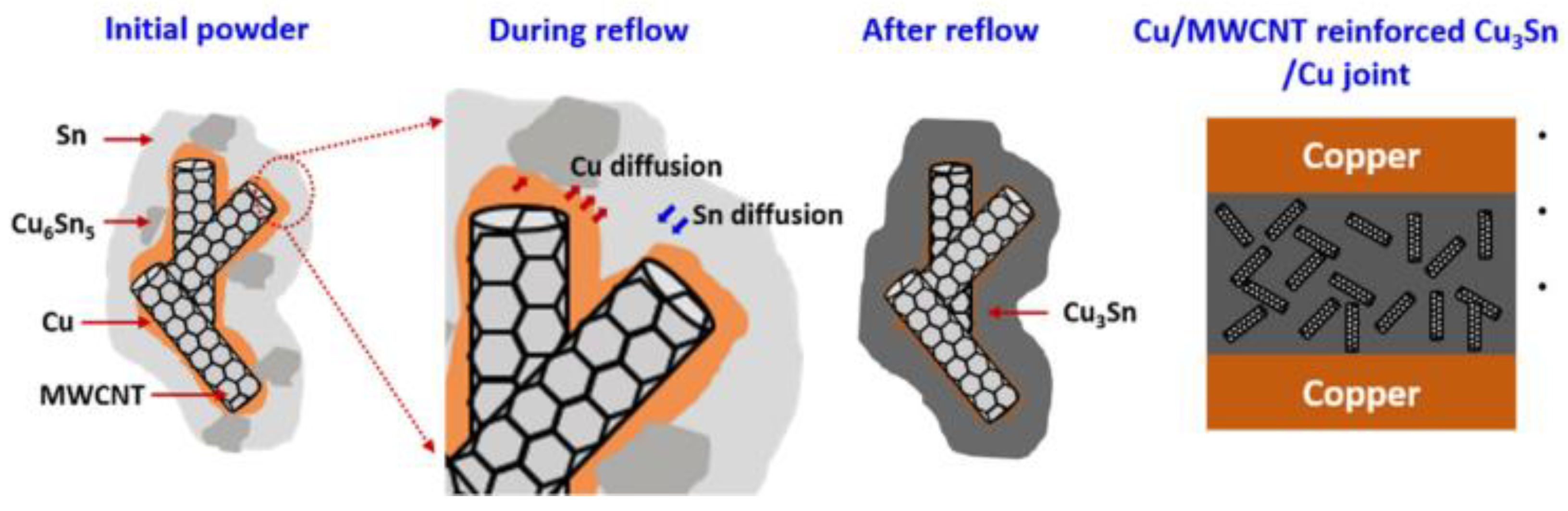
5.3. Composite Fillers

Composite solders such as Sn-coated Cu-CNT have also been applied to reduce bonding time and to improve bonding properties [8], Sn-Bi added Cu particles [51], Sn-coated Cu powders [87], and lead-free epoxy composite solder [76]. Ternary sandwiched structures have also been used, e.g., Cu/Sn/Cu and Ni/Sn/Ni joint, by Chu et al. [69], Ag/Sn/Ag system, by Li et al. [90], and Cu bump/Sn/Cu bump, by Deng et al. [91]. The addition of CNTs has yielded attractive bonding properties [92]. In a recent study, the authors conducted TLP bonding of Cu plate-shaped specimens using Cu-Sn alloy including multiwalled CNTs [8]. The schematic of composite TLP bonding is given in Figure 6.
The use of CNTs is known to give enhanced strength and stable electrical conductivity of the joint [93,94]. The bonding time was shortened 8 min incorporating CNT in the Sn-Cu system and a complete transformation of Cu6Sn5 into Cu3Sn occurred. The joint strength of the Cu/MWCNT + Cu3Sn/Cu junction was measured to be about 35 MPa.
A summary of the shear bond strength after foil and powder type TLP bonding is given in Figure 7. The various bonding specimens and conditions are indicated in Table 2. The bonding temperature, bonding time, and bonding strength of an important specimen are specified.
The Cu/Sn/Cu system showed a lower bonding strength of 0.5 MPa at 280 °C and a very short bonding time of 8 s [71]. The Cu/MWCNT + Cu3Sn/Cu joint specimens studied by the authors and others were balanced in terms of bonding time and strength, with a bonding temperature of 260 °C, a bonding time of 8 min, and a shear strength of 35 MPa [8].
The Sn coated Cu fillers give the joint strength in the range from 20 to 35 MPa [87]. The strengths of powder type solders are in the range between 20 and 40 MPa. Most of the foil type solders provide strength from approximately 20 to 35 MPa [69,70,71,95]. However, the use of ultrasonic energy has been shown to improve shear strength considerably. The joint shear strength was over 60 MPa, and the joint had a very thin Sn layer with a maximum strength of 275 MPa [96,97]. The shear strength of Cu-Cu joints bonded with Sn-coated Cu-CNT powders was reported by the authors in [8]. The joints of Cu/MWCNT + Cu3Sn/Cu systems with solder components of MWCNT and Cu-Sn IMC are expected to strengthen the joints by fiber reinforcement and precipitation hardening. An increase in bonding time at a bonding temperature of 260 °C resulted in enhanced shear strength. The shear strength was 10 MPa after 3 min, which increased to 35.3 MPa after 8 min. The 8 min reflow time was enough to consume the entire Sn at the joint [8].

5.4. Ag Die-Attached Materials

Low-temperature sintering methods have also been studied to obtain TLP bonding stability at high temperatures. Mostly SnSb, SnSb-Ag, Ag, Cu, or the like have been used for die-attach bonding. Among them, SnSb solder mainly uses solid solution strengthening, SnAg solder uses Ag3Sn IMC precipitation strengthening, and SnSb-X solder, etc., uses the solid solution and precipitation strengthening [98]. Ag-based solder, Ag-(0–50 wt.%)Sn, was used for TLP soldering for high-temperature applications by Sharif et al. [80]. However, Ag sintering methods are highly expensive, which encourages cost-effective TLP bonding methods with higher productivity.

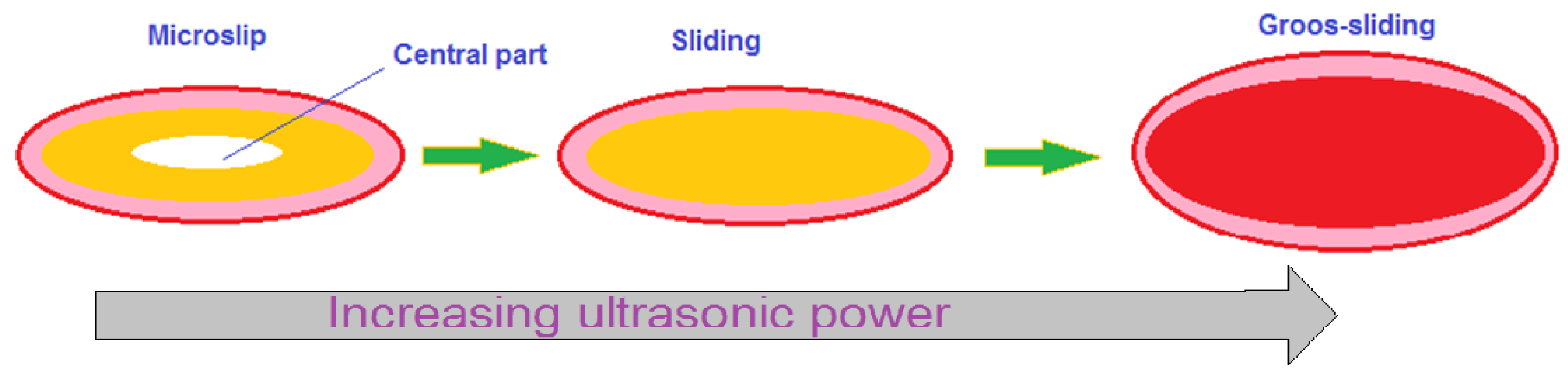
6. Ultrasonic Wire Bonding in Power Devices

Similar to TLP bonding, wire bonding is an essential component of power modules. Wire bonding for the power module mainly uses aluminum wire, aluminum ribbon, copper wire, and aluminum-copper wire. In wire bonding, Al electrodes are bonded to the semiconductor chip (IGBT module) and external lead frames, which are metallic terminals used for electrical connection between the IGBT and the leads. The ultrasonic wire bonding method is categorized into ball bonding (1st bonding) and crescent bonding (ball, wedge, or second bonding) when a capillary is used [99]. Wires difficult to bond with balls, such as aluminum, are joined by wedge bonding using a wedge as a bonding tool, which we review in this report.

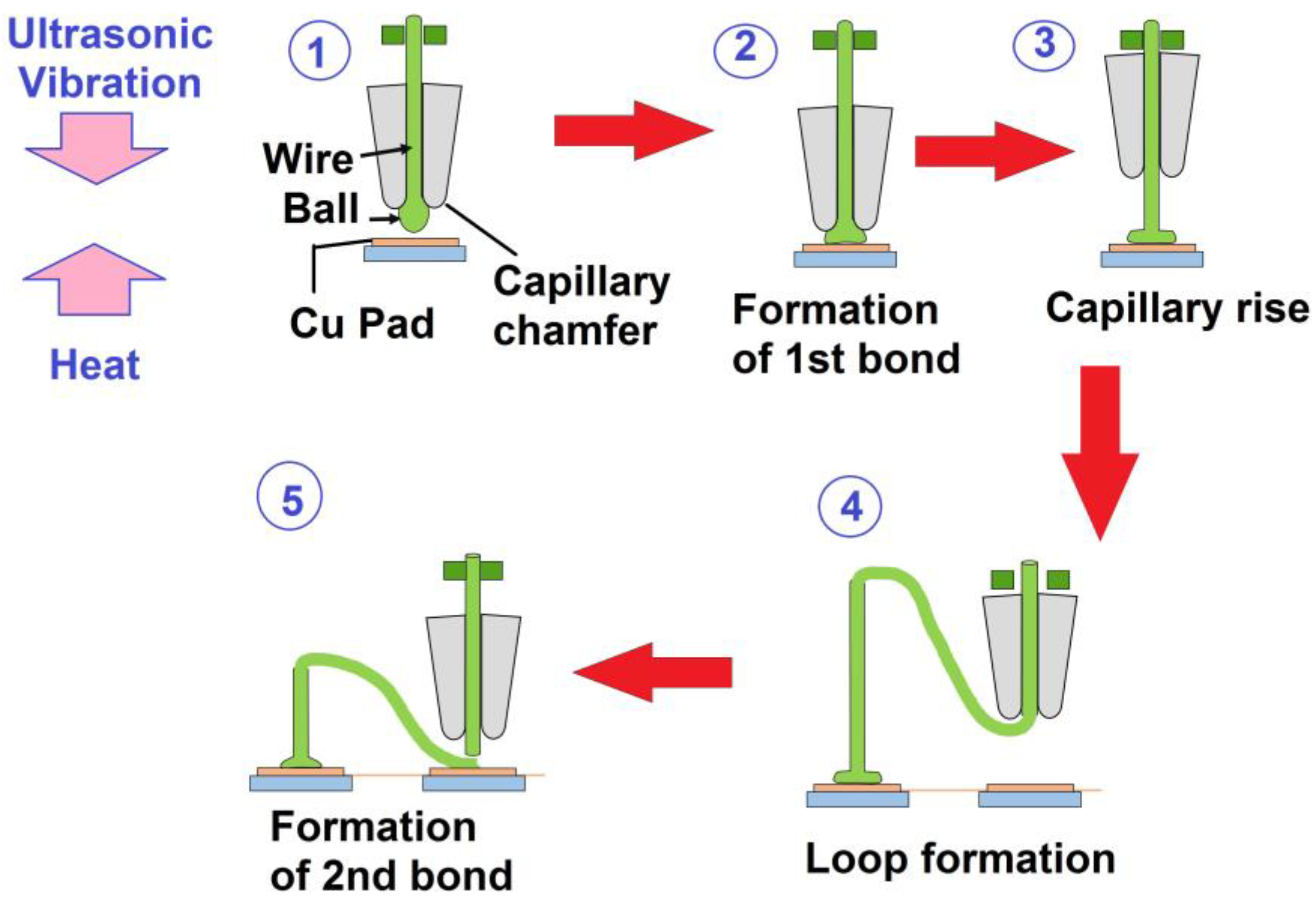
6.1. Ball Bonding or Crescent Bonding
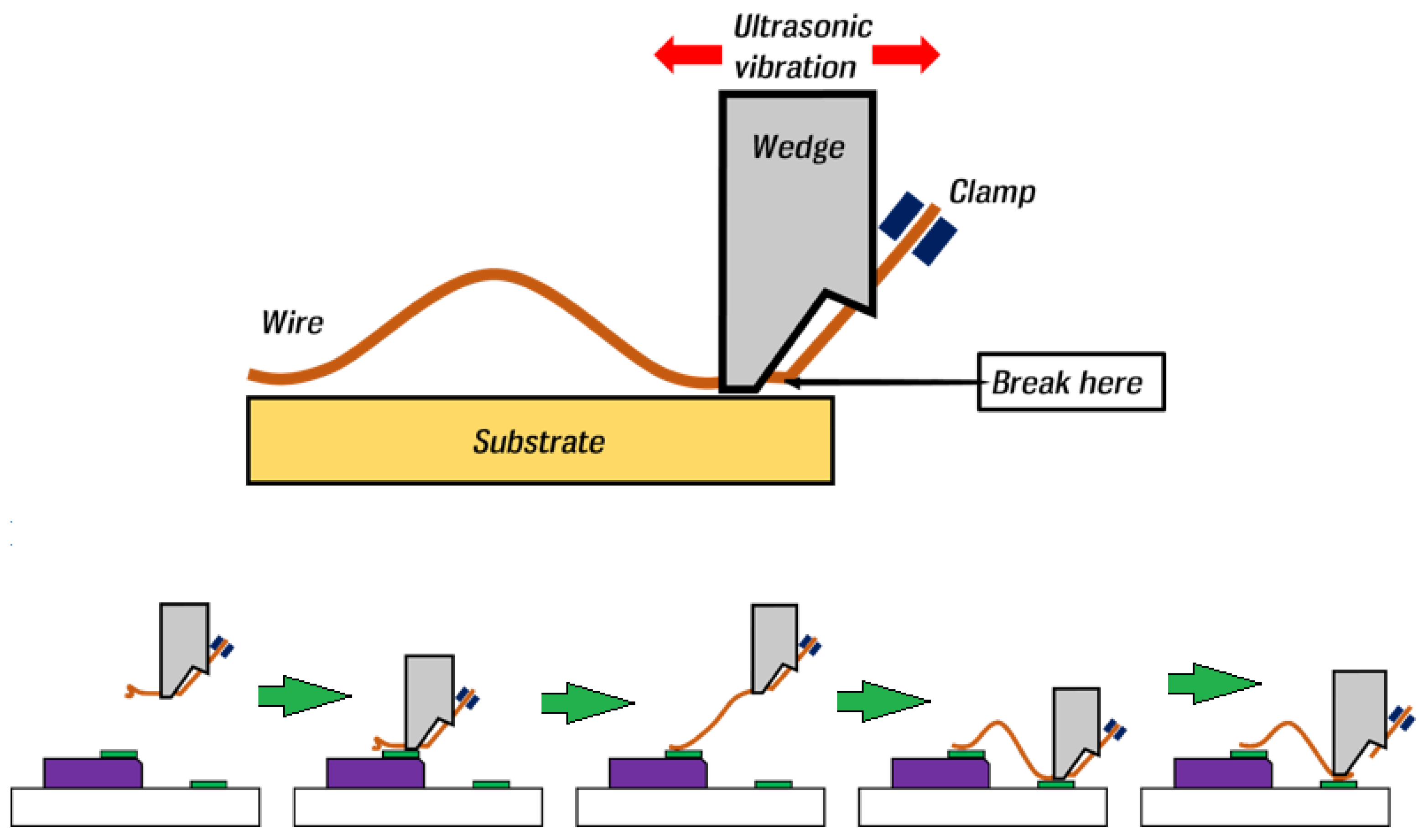
The first step in wire bonding is ball bonding. It is performed by melting the wire at the one terminal supplied through the capillary using an arc between the electrode and the wire terminal to make a ball, and then pressing the aluminum electrode of the chip through ultrasonic waves (Figure 8). In the second step, the Al electrode is pressed, and the capillary is moved over the lead terminal and acquires the proper length through the capillary. The junction at the metal terminal lead uses a tip of the capillary without an arc to press the wire ultrasonically. When the bonding is completed, the wire is fixed with a clump and then pulled to cut [100], as shown in Figure 8.
The schematic for ball bonding or crescent bonding is shown in Figure 9. The authors reported the bonding mechanism in wire bonds, and they found that increasing the ultrasonic output during wire bonding caused a micro slip in the ball area pressed to the electrode pad on the chip if the output was low [100,101].
At this instant, the size of the micro-slip occurring in the circumference of the ball was calculated, as shown in the following equation [101]:
a = a s 1 s μ s N 3
The bonding mechanism consists of three stages, namely friction, approach, and interdiffusion, between a wire and a pad on the substrate [100,101]. As the ultrasonic power increases, the fine slip generally changes to microslip, gross sliding, and final bonding, as shown in Figure 10.
At this stage, the bonding is completed after heating and pressing. The central part indicates the joint after the ball bonding, which is un-bonded, and the outer area is the bonded region [100,101,102,103,104].

6.2. Wedge Bonding

Wedge bonding is also a type of wire bonding, as already described, and widely used in the past for power module joining. Here, Al-wire is compressed by applying ultrasonic waves to electrodes and leads on a chip using a tool called a wedge. The use of ultrasonic waves causes plastic deformation at the bonding interface at room temperature to destroy the oxide film of aluminum. The wire mainly uses Al-1%Si with a diameter of about 25–50 μm, and since the strength of the aluminum wire is low, a gold wire is also used to compensate for this. For example, a fine pitch wedge bonding experiment of 40 μm was conducted using an ultrafine gold alloy with a diameter of 10 μm [105].
The wedge bonding process is shown in Figure 11. First, the aluminum wire on the tip of the wedge is placed on the aluminum electrode of the semiconductor chip with a tool called a "wedge", and ultrasonic waves are impressed. Next, the wire is pulled towards the lead and pressed at the terminal of the wedge by ultrasonic waves followed by pulling and cutting the wire. The deformation of the wire generated at this time severely affects the destruction of the oxide film, the bonding area, and the strength of the bonding portion [105,106].
Wedge bonding usually occurs in a very short time, such as less than a few hundred milliseconds, at ambient temperature. The relative motion between the wire and the pad occurs due to vibrating ultrasonic waves. The suitable ultrasonic frequency depends on the wire type or thickness. Thin Al or Au wires are wedge or ball bonded at 100–140 kHz. Moreover, heavy Al-wire or ribbon can be combined at low frequencies between 40 and 80 kHz. The advantage of the wedge bonding method is that it is a junction between an Al-electrode of a semiconductor chip and a homogeneous metal because mainly aluminum wire is used. There is no issue of forming an IMC at the bonding interface, unlike TLP bonding. Wedge bonding differs from ball bonding in the sense that the bonded area is located at the center in wedge bonds, while in ball-bonding, the central area is usually un-bonded [105].
Lum et al. [105] suggested the ultrasonic bonding model of wedge bonding using an Al wire. They found that at low ultrasonic power (130 mW), microslip became concentrated at the peripheral region but did not reach the center of the footprint (Figure 12). In addition, at higher ultrasonic power (195 mW), gross-slide occurred, and the bonded areas reached the central part of the footprint entirely. By increasing the bonding power further to 260 mW, the bonding density was over-increased, and destruction of the oxide layer occurred.
According to Lum et al. [105], the depth of wear during friction for the wedge coupling mechanism is given by
d = t × K P V H
where d = wear depth, t = the time of relative motion, K = wear coefficient, P = mean pressure, V = sliding speed, and H = material hardness. This ultrasonic friction causes heat generation at the bonding interface, and the compression load results in plastic deformation. At the last stage of wire bonding, the wedge is recrystallized and softened. Furthermore, since the size of the joint is small compared to that of the ball bonding method, it is relatively easy to achieve a fine pitch. However, since the bonding speed per wire is about 0.25 s, which is slower than the ball bonding method, it is somewhat inferior in terms of mass production [99,101,106,107].
Various aluminum wires such as Al, Al-0.5Cu, and Al-0.005Ni wire are used for wire bonding for the IGBT module. It is known that adding copper to an aluminum wire can improve creep properties at high temperatures. Kurosu et al. [108] revealed that Al2Cu precipitates (θ phases) were formed on the aluminum wire base metal through the experiment of alloying copper to the aluminum bonding wire of the IGBT chip, thereby precipitating and strengthening the aluminum wire. They explained that, by heat treatment and aging, very fine Al2Cu phases precipitated on Al matrix and grain boundaries, so that the reliability of the Al-0.5Cu wire was much improved compared to Al wire. From a similar point of view, adding nickel to the aluminum wire can improve the high-temperature strength of the aluminum wire by depositing Al3Ni precipitates on the Al wire base metal [108]. Wire bonding connects electrically between the semiconductor chip and metal pad on a substrate. For wire bonding generally, Au, Cu, Ag, and Al wires are used. In the power module, mostly wedge bonding is preferred, and Al wire, Al ribbon, Cu wire, and Al-Cu wires are frequently adopted for the wedge bonding. In many cases, Al-1%Si wire having a diameter around 25–50 μm is used for the wedge bonding. Heavy wire indicates over 100 μm in diameter for power packages and discrete devices, but fine aluminum wires mean less than 100 μm in diameter, e.g., 18–100 μm. Since Al wire has lower strength, Au wire of diameter of 10 μm has also been tried for bonding a 40 μm pitch in wedge bonding. The recrystallization occurs at the interface region only a few milliseconds after switching on ultrasonic power during the wedge bonding process [109].

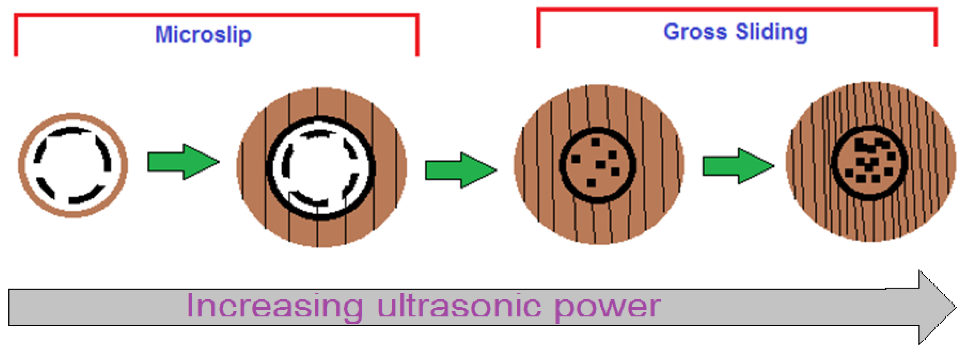
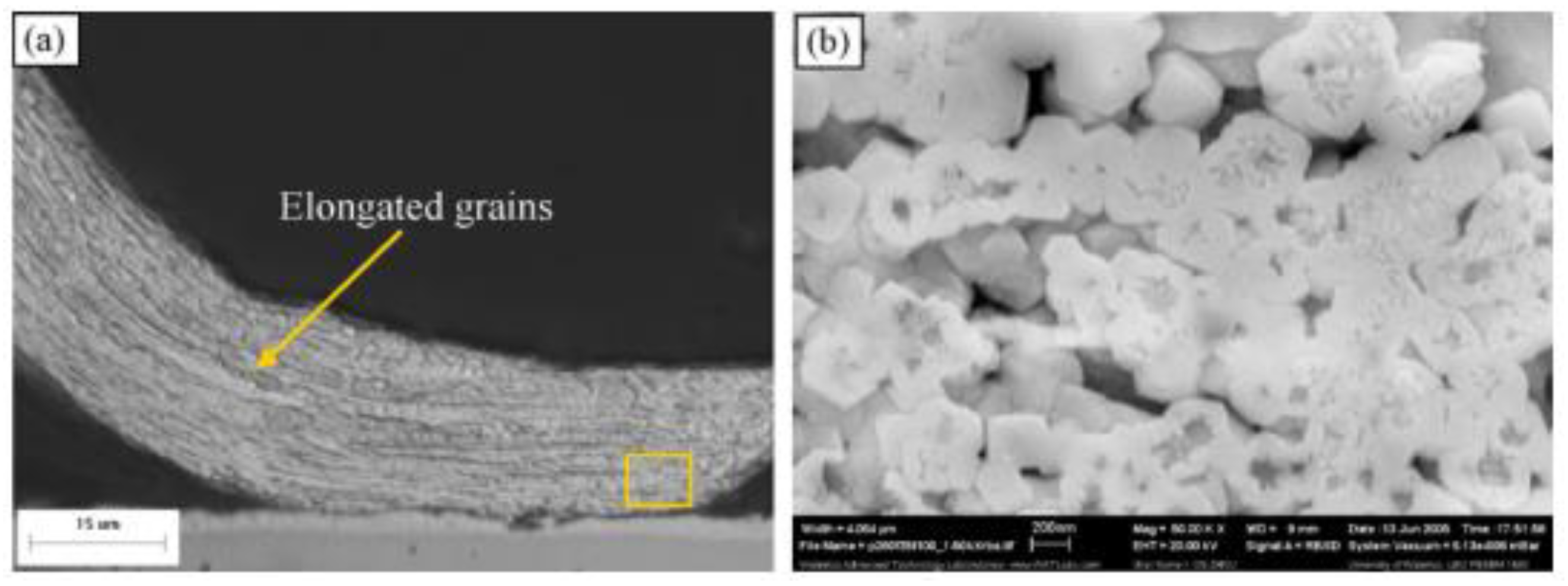
7. Recrystallization in Wedge Bonding

Ultrasonic wire bonding, which includes ball and wedge bonding, is a solid-state joining process. Ultrasonic bonding is completed in a relatively short time where high-frequency ultrasonic energy yields a bond joint between materials to be bonded [110,111,112,113]. During ultrasonic vibration, wear of the metal surface occurs and, consequently, the surface oxide layer is removed. The fine aluminum oxide particles grind and polish the surface, leading to a well-exposed layer on both sides.
Figure 13 shows the cross-section image of the Cu-wire wedge bonded at the ultrasonic power of 325 mW for 50 ms [114]. The recrystallized grains can be observed in the central zone (Figure 13a,b). These elongated grains are formed during the drawing process of Cu wire due to the frictional heating and normal compressive force induced by ultrasonic vibration along the faying surface leading to the recrystallization of grains.
The driving force of the recrystallization, ΔE, between the deformed and recrystallized state is determined by the dislocation density or the sub-grain boundary energy according to the following equation [115]:
Δ E ρ G b 2 3 γ s d s
where ρ = dislocation density, G = shear modulus, b = Burgers vector, γ s is the sub-grain boundary energy, and d s is the sub-grain size.
According to Equation (7), the recrystallization temperature depends on annealing time, amount of cold work, grain size, and material composition. Normally, the recrystallization temperature of pure metal is known to be in the range of about 0.3 to 0.4 Tm and that of the alloy is around 0.5 Tm, where Tm is a melting point [116,117]. The heat produced due to deformation at the bonding interface during ultrasonic wire bonding comes from the power dissipated over the weld, and it can be calculated as the following equation [117,118]:
Q w = P A w F w × V a v g A w
where Q w = heat flux due to deformation in W m 2 , P = power in W, A w = weld area in m 2 , F w = weld force in N, V a v g = average sonotrode velocity = 4 × ε 0 × f w , ε 0 being the amplitude of vibrations, and f w = welding frequency.
Q w = ( Y γ 2 ) 2 ( F N / A D Z 2 ) 2 × 4 × ε 0 × f w
where Y γ = average temperature-dependent yield strength in N m 2 , F N = clamping force in N, and A D Z = deformed area in m 2 . Jedrasiak et al. [117] calculated temperature during ultrasonic welding of Al 6111 alloys to dissimilar metals by the finite element model. For a smaller clamping force, the interface temperatures are calculated as 79.26 °C, 117.8 °C, and 141.2 °C, respectively. The microstructural model successfully predicted the thickness of the IMC layer at the Al-Mg interface. The IMC thickness increases with ultrasonic bonding time, and the IMC thickness at the bonding center area is thicker than the peripheral area. Chen et al. [118] also calculated temperature distribution during the ultrasonic welding of Cu and Al by the 3D finite element model. They suggested the temperature was highest around the central bonding area under the solenoid tip. Other researchers also reported the temperature at the bonding interface of ultrasonic boding [119,120,121]. To reduce the friction between ultrasonic interfaces, authors have used soft and ductile Sn-3.5%Ag alloy and obtained a maximum temperature of 80 °C at ultrasonic power of 1.4 kW [122].

8. Reliability Studies

Wire bonding has been used widely and is an important component in power electronics. The advantage of wire bonding in the era of miniaturization cannot be ignored. Various reliability issues of wire bonding have been reported. Park et al. [115] studied Al wedge bonding using 152.4 μm and 381.0 μm thick wires bonded to an Al-metalized Si chip. The reliability testing was conducted at high-temperature high humidity tests (TH) (85 ± 3 °C, 85 ± 3 RH for 1000 h) under a thermal shock (TS) range of −40–125 °C, 10 min. They suggested that thermal shock tests were more severe than the TH, and to evaluate the deterioration rate of the wire in a short time, it was found that the discrimination power of TS was superior to TH.
However, when the wire diameter was as thin as 152.4 μm, the bonding strength of the wire joint was smaller than the tensile strength of the wire itself, and the bonding strength could be measured. However, at a wire diameter of 381.0 μm, the tensile strength of the wire was smaller than the bonding strength, and the bonding strength could not be measured. Therefore, this method works accurately for the thinner wire diameter [115].

9. Conclusions

In this paper, the TLP bonding method and the wire bonding method required for power module manufacturing were overviewed. The TLP bonding method using Sn-based solder was more advantageous due to the low-temperature and cost-effective process but has the drawback of the formation of brittle IMCs after bonding. Various studies have been conducted to improve these shortcomings, and in addition to simple bond strength evaluation for joints, in-depth studies have been conducted in various fields such as various aging strength characteristics, warpage deformation, and electrical and thermal characteristics. Even though packaging technology meets the miniaturization requirements of semiconductors in various fields due to its flexibility, price competitiveness, and the great advantages of existing infrastructure, wire bonding technology is still attracting attention in the packaging field. To manufacture high-reliability power modules for next-generation devices, it is expected that various and in-depth studies on the bonding method and reliability introduced in this paper will continue.

10. Future Directions and Outlook

TLP bonding is an economical process, as compared to Ag die-attached materials, that could replace Pb-Sn solders. TLP bonding has been successfully applied to various forms of Sn-based solders in bulk, powder, paste, or foil forms. However, there is always a need to bring down the bonding time by alloying additions to the solder. Higher solidification times may lead to undesirable intermetallic compounds at the joint. Advanced alloys have been developed such as cheaper Zn-based solder, and composite bonding materials reinforced with carbon nanotubes and nanoparticles. However, proper dispersion of these reinforcements is essential to achieve maximum benefits. Novel alloys discovered in the last decade are supposed to prevent intermetallic compound formation due to high mixing entropy. Such high entropy alloys can also be recommended for TLP bonding in the future. Similarly, due to advancements in electronic packaging, wire bonding is still being applied in power module joining. However, more research is needed to analyze the joint strength of the wire and wedge bonding concerning ceramic-metal power module joining.

Author Contributions

Conceptualization and methodology, H.K.; formal analysis and validation, A.S.; resources and supervision, J.P.J.; writing—original draft preparation, H.K.; writing—review and editing, J.P.J. All authors have read and agreed to the published version of the manuscript.

Funding

This work was supported by Nano-Convergence Foundation (www.nanotech2020.org) funded by the Ministry of Science and ICT (MSIT, Korea) and the Ministry of Trade, Industry and Energy (MOTIE, Korea) (project name: Development of high-ductility, low temperature nano-dispersion solder paste technology for automotive electronics and flexible devices; project Number: R202000210).

Conflicts of Interest

The authors declare no conflict of interest.

References

  1. Sharma, A.; Lee, J.H.; Kim, K.H.; Jung, J.P. Recent advances in thermoelectric power generation technology. J. Microelectron. Packag. Soc. 2017, 24, 9–16. [Google Scholar] [CrossRef] [Green Version]
  2. Sharma, A.; Das, S.; Das, K. Pulse electrodeposition of lead-free tin-based composites for microelectronic packaging. In Electrodeposition of Composite Materials; Mohamed, A.A.A., Golden, T.D., Eds.; InTech: Rijeka, Croatia, 2016; Volume 3, pp. 253–274. [Google Scholar]
  3. Chen, C.; Luo, F.; Kang, Y. A review of SiC power module packaging: Layout material system and integration. CPSS TPEA 2017, 2, 170–186. [Google Scholar] [CrossRef]
  4. Brambilla, A.; Dallago, E.; Romano, R. Analysis of an IGBT power module. In Proceedings of the IEEE 20th International Conference on Industrial, Electronics, Control and Instrumentation, Bologna, Italy, 5–9 September 1994; IEEE: Bologna, Italy, 1994; pp. 129–134. [Google Scholar]
  5. Pithadia, S.; Kumar, N. Analysis of Power Supply Topologies for IGBT Gate Drivers in Industrial Drives(SLAA672); Application Report for Texas Instruments; Texas Instruments: Dallas, TX, USA, 2015. [Google Scholar]
  6. Cooper, J.A.; Melloch, M.R.; Singh, R.; Agarwal, A.; Palmour, J.W. Status and prospects for SiC power MOSFETs. IEEE Trans. Electron Devices 2002, 49, 658–664. [Google Scholar] [CrossRef]
  7. Roh, M.H.; Nishikawa, H.; Jung, J.P. A review of Ag paste bonding for automotive power device packaging. J. Microelectron. Packag. Soc. 2015, 22, 15–23. [Google Scholar] [CrossRef] [Green Version]
  8. Rajendran, S.H.; Jung, D.H.; Cheon, W.S.; Jung, J.P. Transient liquid phase bonding of copper using Sn coated Cu MWCNT composite powders for power electronics. Appl. Sci. 2019, 9, 529. [Google Scholar] [CrossRef] [Green Version]
  9. Roh, M.H.; Nishikawa, H.; Jung, J.P.; Kim, W.J. Transient liquid phase bonding for power module packaging. J. Microelectron. Packag. Soc. 2017, 24, 27–34. [Google Scholar] [CrossRef] [Green Version]
  10. Al-Hazaa, A.N.; Muhammad, A.S.; Shar, A.; Atieh, A.M.; Nishikawa, H. Transient liquid phase bonding of magnesium alloy AZ31 using Cu coatings and Cu coatings with Sn interlayers. Metals 2018, 8, 60. [Google Scholar] [CrossRef] [Green Version]
  11. Norrish, J. Advanced Welding Processes, 2nd ed.; Woodhead Publishing: Cambridge, UK, 2006; p. 2. [Google Scholar]
  12. Choi, D.Y.; Sharma, A.; Uhm, S.H.; Jung, J.P. Liquid metal embrittlement of resistance spot welded 1180 TRIP steel: Effect of electrode force on cracking behavior. Met. Mater. Int. 2018, 25, 219. [Google Scholar] [CrossRef]
  13. Sharma, A.; Lim, D.U.; Jung, J.P. Microstructure and brazeability of SiC nanoparticles reinforced Al-9Si-20Cu produced by induction melting. Mater. Sci. Technol. 2016, 32, 773. [Google Scholar] [CrossRef]
  14. Sharma, A.; Das, S.; Das, K. Pulse Electroplating of Ultrafine Grained Tin Coating. In Electroplating of Nanostructures; Aliofkhazraei, M., Ed.; Intechopen: Rijeka, Croatia, 2015. [Google Scholar]
  15. Sharma, A.; Mallik, S.; Ekere, N.N.; Jung, J.P. Printing morphology and rheological characteristics of lead-free Sn-3Ag-0.5 Cu (SAC) solder pastes. J. Microelectron. Packag. Soc. 2014, 21, 83. [Google Scholar] [CrossRef] [Green Version]
  16. Sharma, A.; Kee, S.H.; Jung, F.; Heo, Y.; Jung, J.P. Compressive strength evaluation in brazed ZrO2/Ti6Al4V joints using finite element analysis. J. Mater. Eng. Perform. 2016, 25, 1722. [Google Scholar] [CrossRef]
  17. Kolenak, R.; Kostolny, I.; Drapala, J.; Zackova, P.; Kuruc, M. Direct ultrasonic soldering of AlN ceramics with copper substrate using Zn-Al-Mg solder. Metals 2020, 10, 160. [Google Scholar] [CrossRef] [Green Version]
  18. Prach, M.; Kolenak, R. Soldering of copper with high-temperature Zn-based solders. Procedia Eng. 2015, 100, 1370. [Google Scholar] [CrossRef] [Green Version]
  19. Rettenmayr, M.; Lambracht, P.; Kempf, B.; Tschudin, C. Zn-Al based alloys as Pb-free solders for die attach. J. Electron. Mater. 2002, 31, 278–285. [Google Scholar] [CrossRef]
  20. Shimizu, T.; Ishikawa, H.; Ohnuma, I.; Ishida, K. Zn-Al-Mg-Ga Alloys as Pb-free solder for die-attaching use. J. Electron. Mater. 1999, 28, 1172–1175. [Google Scholar] [CrossRef]
  21. Cheng, F.; Gao, F.; Wang, Y.; Wu, Y.; Ma, Z.; Yang, J. Sn addition on the tensile properties of high temperature Zn-4Al-3Mg solder alloys. Microelectron. Reliab. 2012, 52, 579–584. [Google Scholar] [CrossRef]
  22. Cui, W.; Yan, J.; Dai, Y.; Li, D. Building a nano-crystalline-alumina layer at a liquid metal/sapphire interface by ultrasound. Ultrason. Sonochem. 2015, 22, 108–112. [Google Scholar] [CrossRef]
  23. Mishra, S.; Sharma, A.; Jung, D.H.; Jung, J.P. Recent advances in active metal brazing of ceramics and process. Met. Mater. Int. 2019, in press. [Google Scholar] [CrossRef]
  24. Sharma, A.; Ahn, B. Brazeability, microstructure and joint characteristics of ZrO2/Ti-6Al-4V brazed by Ag-CuTi filler reinforced with cerium oxide nanoparticles. AMSE 2019, 2019, 11. [Google Scholar] [CrossRef] [Green Version]
  25. Sharma, A. High-Entropy Alloys for Micro- and Nanojoining Applications. In Engineering Steels and High Entropy-Alloys; Sharma, A., Ed.; Intechopen: Rijeka, Croatia, 2020. [Google Scholar]
  26. Sharma, A.; Kumar, S.; Duriagina, Z. (Eds.) Engineering Steels and High Entropy-Alloys; IntechOpen: Rijeka, Croatia, 2020. [Google Scholar]
  27. Srivastava, A.K.; Sharma, A. Advances in joining and welding technologies for automotive and electronic applications. Am. J. Mater. Eng. Technol. 2017, 5, 7–13. [Google Scholar] [CrossRef] [Green Version]
  28. Schwartz, M.M. Brazing, 2nd ed.; ASM International: Novelty, OH, USA, 2003. [Google Scholar]
  29. Gale, W.F.; Butts, D.A. Transient liquid phase bonding. Sci. Technol. Weld. Join. 2004, 9, 283–300. [Google Scholar] [CrossRef]
  30. Weyrich, N.; Leinenbach, C. Low temperature TLP bonding of Al2O3-ceramics using eutectic Au-(Ge, Si) alloys. J. Mater. Sci. 2013, 48, 7115–7124. [Google Scholar] [CrossRef] [Green Version]
  31. Hoppin, G.S.; Berry, T.F. Activated diffusion bonding. Weld. J. 1970, 49, 505–509. [Google Scholar]
  32. Duvall, D.S.; Owczarski, W.A.; Paulonis, D.F. Transient liquid phase bonding: A new method for joining heat resistant alloys. Weld. J. 1974, 53, 203–214. [Google Scholar]
  33. Jung, J.P.; Kang, C.S. Transient liquid phase process in Ni-B joining. Mater. Trans. 1997, 38, 886–891. [Google Scholar] [CrossRef] [Green Version]
  34. Jung, J.P.; Kang, C.S. Liquid metal formation of Ni/B/Ni diffusion bonded joint. J. Korean. Inst. Met. Mater. 1995, 33, 1302–1308. [Google Scholar]
  35. Jung, J.P.; Kang, C.S. A study on the width of liquid layer of Ni/B/Ni diffusion bonding system. J. Korean. Weld. Soc. 1995, 13, 402–409. [Google Scholar]
  36. Jung, J.P.; Kang, C.S. Mechanical property of liquid phase diffusion bonded joint of Rene80/B/Rene80. J. Korean. Weld. Soc. 1995, 13, 125–133. [Google Scholar]
  37. Jung, J.P.; Kang, C.S. Liquid phase diffusion bonding procedure of Rene80/B/Rnene80 system. J. Korean. Weld. Soc. 1995, 13, 172–178. [Google Scholar]
  38. Jung, J.P.; Kang, C.S. Liquid phase diffusion bonding of Rene80 using pure boron. Mater. Trans. 1996, 37, 1008–1013. [Google Scholar] [CrossRef] [Green Version]
  39. Jung, J.P.; Lee, C.D.; Kang, C.S. A study on the melting induced bonding of 304 stainless steel. J. Korean. Inst. Met. Mater. 1993, 31, 323–329. [Google Scholar]
  40. Cook III, G.O.; Sorensen, C.D. Overview of transient liquid phase and partial transient liquid phase bonding. J. Mater. Sci. 2011, 46, 5305. [Google Scholar] [CrossRef] [Green Version]
  41. Chang, S.Y.; Huang, Y.H.; Tsao, L.C. Active solders and active soldering. In Fillers-Synthesis, Characterization and Industrial Application; Patnaik, A., Ed.; IntechOpen: Rijeka, Croatia, 2019. [Google Scholar]
  42. Lis, A.; Leinenbach, C. Effect of process and service conditions on TLP-bonded components with (Ag,Ni–)Sn interlayer combinations. J. Electron. Mater. 2015, 44, 4576–4588. [Google Scholar] [CrossRef]
  43. Tollefsen, T.A.; Larsson, A.; Lřvvik, O.; Aasmundtveit, K. Au-Sn SLID bonding—Properties and possibilities. Metall. Mater. Trans. B 2012, 43, 397–405. [Google Scholar] [CrossRef]
  44. Nobeen, N.S.; Imade, R.; Lee, B.; Phua, E.; Wong, C.; Gan, C. Transient liquid phase (TLP) bonding using Sn/Ag multilayers for high temperature applications. In Proceedings of the IEEE 15th Electronics Packaging Technology Conference (EPTC 2013), Singapore, 11–13 December 2013; IEEE: Singapore, 2013; p. 647. [Google Scholar]
  45. Yoon, S.W.; Glover, M.D.; Shiozaki, K. Nickel-tin transient liquid phase bonding toward high-temperature operational power electronics in electrified vehicles. IEEE Trans. Power Electron. 2013, 28, 2448. [Google Scholar] [CrossRef]
  46. Honrao, C.; Huang, T.C.; Kobayashi, M.; Smet, V.; Raj, P.M.; Tummala, R. Accelerated SLID bonding using thin multi-layer copper-solder stack for fine-pitch interconnections. In Proceedings of the IEEE 64th Electronic Components and Technology Conference (ECTC), Orlando, FL, USA, 27–30 May 2014; IEEE: Orlando, FL, USA, 2014; p. 1160. [Google Scholar]
  47. Bajwa, A.; Wilde, J. Reliability modeling of SnAg transient liquid phase die-bonds for high-power SiC devices. Microelectron. Reliab. 2016, 60, 116. [Google Scholar] [CrossRef]
  48. Bajwa, A.A.; Qin, Y.Y.; Zeiser, R.; Wilde, J. Foil based transient liquid phase bonding as a die-attachment method for high temperature devices. In Proceedings of the CIPS 8th International Conference on Integrated Power Electronics Systems, Nuremberg, Germany, 25–27 February 2014; VDE Verlag Gmbh: Berlin, Germany, 2014; p. 1. [Google Scholar]
  49. Liu, B.; Tian, Y.; Feng, J.; Wang, C. Enhanced shear strength of Cu-Sn intermetallic interconnects with interlocking dendrites under fluxless electric current-assisted bonding process. J. Mater. Sci. 2017, 52, 1943. [Google Scholar] [CrossRef]
  50. Shao, H.; Wu, A.; Bao, Y.; Zhao, Y.; Zou, G. Interfacial reaction and mechanical properties for Cu/Sn/Ag system low temperature transient liquid phase bonding. J. Mater. Sci. 2016, 27, 4839–4848. [Google Scholar] [CrossRef] [Green Version]
  51. Mokhtari, O.; Nishikawa, H. The shear strength of transient liquid phase bonded Sn-Bi solder joint with added Cu particles. Adv. Powder Technol. 2016, 27, 1000–1005. [Google Scholar] [CrossRef]
  52. Greve, H.; Moeini, S.A.; McCluskey, F.P. Reliability of paste based transient liquid phase sintered interconnects. In Proceedings of the IEEE 64th Electronic Components and Technology Conference (ECTC), Orlando, FL, USA, 27–30 May 2014; IEEE: Orlando, FL, USA, 2014; p. 1314. [Google Scholar]
  53. Zhao, H.Y.; Liu, J.H.; Li, Z.L.; Zhao, Y.X.; Niu, H.W.; Song, X.G.; Dong, H.J. Non-interfacial growth of Cu3Sn in Cu/Sn/Cu joints during ultrasonic-assisted transient liquid phase soldering process. Mater. Lett. 2017, 186, 283. [Google Scholar] [CrossRef]
  54. Ji, H.; Qiao, Y.; Li, M. Rapid formation of intermetallic joints through ultrasonic-assisted die bonding with Sn-0.7Cu solder for high temperature packaging application. Scr. Mater. 2016, 110, 19–23. [Google Scholar] [CrossRef]
  55. Ji, H.; Li, M.; Ma, S.; Li, M. Ni 3 Sn 4-composed die bonded interface rapidly formed by ultrasonic-assisted soldering of Sn/Ni solder paste for high-temperature power device packaging. Mater. Des. 2016, 108, 590–596. [Google Scholar] [CrossRef]
  56. Liu, X.; He, S.; Nishikawa, H. Thermally stable Cu3Sn/Cu composite joint for high-temperature power device. Scr. Mater. 2016, 110, 101–104. [Google Scholar] [CrossRef]
  57. Hu, T.; Chen, H.; Li, M. Die attach materials with high remelting temperatures created by bonding Cu@Sn microparticles at lower temperatures. Mater. Des. 2016, 108, 383–390. [Google Scholar] [CrossRef]
  58. Yang, T.L.; Aoki, T.; Matsumoto, K.; Toriyama, K.; Horibe, A.; Mori, H.; Orii, Y.; Wu, J.Y.; Kao, C.R. Full intermetallic joints for chip stacking by using thermal gradient bonding. Acta Mater. 2016, 113, 90–97. [Google Scholar] [CrossRef]
  59. Khaja, A.S.; Kaestle, C.; Reinhardt, A.; Franke, J. Optimized thin-film diffusion soldering for power-electronics production. In Proceedings of the 36th International Spring Seminar on Electronics Technology, Alba Iulia, Romania, 8–12 May 2013; IEEE: Alba Lulia, Romania, 2013; p. 11. [Google Scholar]
  60. Greve, H.; Chen, L.Y.; Fox, I.; McCluskey, F.P. Transient liquid phase sintered attach for power electronics. In Proceedings of the IEEE 63rd Electronic Components and Technology Conference, Las Vegas, NV, USA, 28–31 May 2013; IEEE: Las Vegas, NV, USA, 2013; p. 435. [Google Scholar]
  61. Ehrhardt, C.; Hutter, M.; Oppermann, H.; Lang, K.D. A lead free joining technology for high temperature interconnects using Transient Liquid Phase Soldering (TLPS). In Proceedings of the IEEE 64th Electronic Components and Technology Conference (ECTC), Orlando, FL, USA, 27–30 May 2014; IEEE: Orlando, FL, USA, 2014; p. 1321. [Google Scholar]
  62. Hosseinzaei, B.; Ali, R.K.R. Transient liquid phase bonding in the Cu-Sn system. Solder. Surf. Mt. Technol. 2019, 31, 221–226. [Google Scholar] [CrossRef]
  63. Choudhury, S.F.; Ladani, L. Local shear stress strain response of Sn-3.5Ag/Cu solder joint with high fraction of intermetallic compounds: Experimental analysis. J. Alloys Compd. 2016, 680, 665–676. [Google Scholar] [CrossRef] [Green Version]
  64. Sohn, S.; Kim, D.; Kim, H.; Kang, N. Strategies to reduce transient liquid phase bonding time for the die attach of power semiconductors. JWJ 2020, 38, 158–165. [Google Scholar] [CrossRef]
  65. Jung, J.P.; Kang, C.S.; Lee, B.Y. Melting induced diffusion bonding of Rene80 superalloys using boron doping method. JWJ 1991, 9, 26–33. [Google Scholar]
  66. Shao, H.K.; Wu, A.; Bao, Y.; Zhao, Y.; Zou, G. Mechanism of Ag3Sn grain growth in Ag/Sn transient liquid phase soldering. Trans. Nonferrous Met. Soc. China 2017, 27, 722–732. [Google Scholar] [CrossRef]
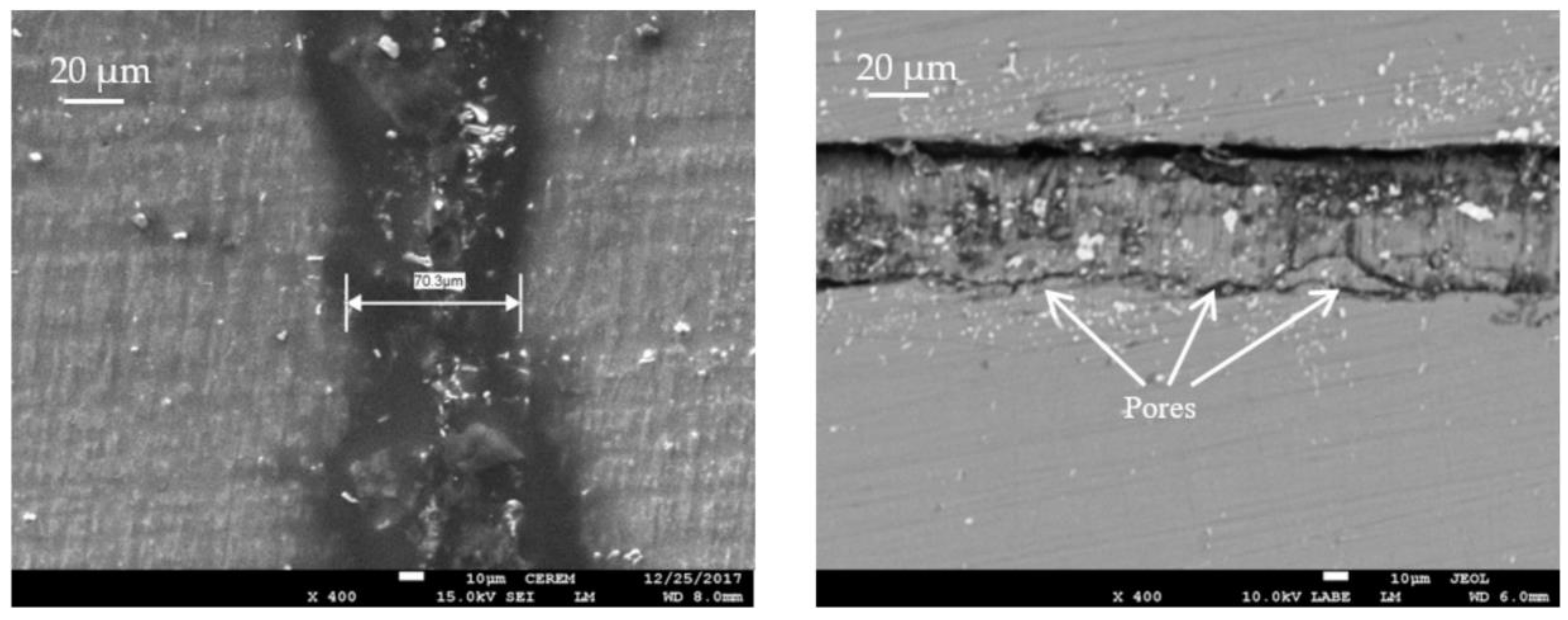
  67. Mokhtari, O. A review: Formation of voids in solder joint during the transient liquid phase bonding process—Causes and solutions. Microelectron. Reliab. 2019, 98, 95–105. [Google Scholar] [CrossRef]
  68. Jung, D.H.; Sharma, A.; Mayer, M.; Jung, J.P. A review on recent advances in transient liquid phase (TLP) bonding for thermoelectric power module. Rev. Adv. Mater. Sci. 2018, 53, 147–160. [Google Scholar] [CrossRef] [Green Version]
  69. Chu, K.; Sohn, Y.; Moon, C. A comparative study of Cn/Sn/Cu and Ni/Sn/Ni solder joints for low temperature stable transient liquid phase bonding. Scr. Mater. 2015, 109, 113–117. [Google Scholar] [CrossRef]
  70. Shao, H.; Wu, A.; Bao, Y.; Zhao, Y.; Zou, G.; Liu, L. Novel transient liquid phase bonding through capillary action for high temperature power devices packaging. Mater. Sci. Eng. A 2018, 724, 231–238. [Google Scholar] [CrossRef]
  71. Brincker, M.; Sohl, S.; Eisele, R.; Popok, V.N. Strength and reliability of low temperature transient liquid phase bonded Cu-Sn-Cu interconnects. Microelectron. Reliab. 2017, 76, 378–382. [Google Scholar] [CrossRef]
  72. Zhao, H.Y.; Liu, J.H.; Li, Z.L.; Song, X.G.; Zhao, Y.X.; Niu, H.W.; Tian, H.; Dong, H.J.; Feng, J.C. A Comparative Study on the Microstructure and Mechanical Properties of Cu6Sn5 and Cu3Sn Joints Formed by TLP Soldering With/Without the Assistance of Ultrasonic Waves. Metall. Mater. Trans. A 2018, 49, 2739–2749. [Google Scholar] [CrossRef]
  73. Elmer, J.W.; Mulay, R.P.; Elmer, J. Superplastic creep of AuSn eutectic solder alloy. Scr. Mater. 2016, 120, 14–18. [Google Scholar]
  74. Zhu, Z.X.; Li, C.C.; Liao, L.L.; Liu, C.K.; Kao, C.R. Au-Sn bonding material for the assembly of power integrated circuit module. J. Alloys Compd. 2016, 671, 340–345. [Google Scholar] [CrossRef]
  75. Peng, J.; Wang, R.C.; Wang, M.; Liu, H.S. Interfacial Microstructure Evolution and Shear Behavior of Au-Sn/Ni-xCu Joints at 350C. J. Electron. Mater. 2017, 46, 2021–2029. [Google Scholar] [CrossRef]
  76. Sharma, A.; Jung, D.H.; Cheon, J.S.; Jung, J.P. Epoxy polymer solder pastes for micro-electronic packaging applications. JWJ 2019, 37, 7–14. [Google Scholar] [CrossRef] [Green Version]
  77. Dong, Y.Y.; Son, J.H.; Ko, Y.H.; Lee, C.W.; Dongjin, B.; Bang, J. A Study on Joint Properties of Sn-Cu-(X)Al-(Y)Si/Cu Solder by Multiple Reflow. JWJ 2020, 38, 131–137. [Google Scholar]
  78. Corbin, S.F. High-temperature variable melting point Sn-Sb lead-free solder pastes using transient liquid-phase powder processing. J. Electron. Mater. 2005, 34, 1016–1025. [Google Scholar] [CrossRef]
  79. Chidambaram, V.; Hattel, J. Hald, High-temperature lead-free solder alternatives. Microelectron. Eng. 2011, 88, 981–989. [Google Scholar] [CrossRef]
  80. Sharif, A.; Gan, C.L.; Chen, Z. Transient liquid phase Ag-based solder technology for high-temperature packaging applications. J. Alloys Compd. 2014, 587, 365–368. [Google Scholar] [CrossRef]
  81. Fujino, M.; Narusawa, H.; Kuramochi, Y.; Higurashi, E.; Suga, T.; Shiratori, T.; Mizukoshi, M. Transient liquid-phase sintering using tin and silver powder mixture for die bonding. In Proceedings of the International Conference on Solid State Devices and Materials, Sapporo, Japan, 27–30 September 2015; The Japan Society of Applied Physics: Tokyo, Japan, 2015; pp. 60–61. [Google Scholar]
  82. Bao, Y.D.; Wu, A.P.; Shao, H.K.; Zhao, Y.; Liu, L.; Zou, G.S. Microstructural evolution and mechanical reliability of transient liquid phase sintered joint during thermal aging. J. Mater. Sci. 2019, 54, 765–776. [Google Scholar] [CrossRef]
  83. Saud, N.; Said, R.M. Transient liquid phase bonding for solder-a short review. IOP Conf. Ser. Mater. Sci. Eng. 2019, 701, 012050. [Google Scholar] [CrossRef]
  84. Greve, H.; Moeini, S.A.; McCluskey, P.; Joshi, S. Prediction and mitigation of vertical cracking in high-temperature transient liquid phase sintered joints by thermomechanical simulation. J. Electron. Packag. 2018, 140, 020903. [Google Scholar] [CrossRef] [Green Version]
  85. Lang, F.; Yamaguchi, H.; Nakagawa, H.; Sato, H. Thermally stable bonding of SiC devices with ceramic substrates: Transient liquid phase sintering using Cu/Sn powders. J. Electrochem. Soc. 2013, 160, 315–319. [Google Scholar] [CrossRef]
  86. Sun, L.; Chen, M.H.; Zhang, L. Microstructure evolution and grain orientation of IMC in Cu-Sn TLP bonding solder joints. J. Alloys Compd. 2019, 786, 677–687. [Google Scholar] [CrossRef]
  87. Liu, X.; He, S.; Nishikawa, H. Low temperature solid-state bonding using Sn-coated Cu particles for high temperature die attach. J. Alloys Compd. 2017, 695, 2165–2172. [Google Scholar] [CrossRef]
  88. Tatsumi, H.; Lis, A.; Yamaguchi, H.; Matsuda, T.; Sano, T.; Kashiba, Y.; Hirose, A. Evolution of transient liquid-phase sintered Cu–Sn skeleton microstructure during thermal aging. Appl. Sci. 2019, 9, 157. [Google Scholar] [CrossRef] [Green Version]
  89. Yang, L.; Yang, Y.; Zhang, Y.; Xu, F.; Jian, Q.; Lu, W. Microstructure evolution and mechanical properties of the In-Sn-20Cu composite particles TLP bonding solder joints. Appl. Phys. A 2020, 126, 343. [Google Scholar] [CrossRef]
  90. Li, J.F.; Agyakwa, J.F.; Johnson, C.M. Kinetics of Ag3Sn growth in Ag-Sn-Ag system during transient liquid phase soldering process. Acta Mater. 2010, 58, 3429–3443. [Google Scholar] [CrossRef]
  91. Deng, X.; Chawla, N. A study on the bonding process of Cu bump/Sn/Cu bump bonding structure for 3D packaging applications. Acta Mater. 2004, 52, 4291–4330. [Google Scholar] [CrossRef]
  92. Nai, S.M.L.; Wei, J.; Gupta, M. Interfacial intermetallic growth and shear strength of lead-free composite solder joints. J. Alloys Compd. 2009, 473, 100–106. [Google Scholar] [CrossRef]
  93. Yim, B.S.; Lee, J.I.; Kim, J.M. Reliability properties of carbon nanotube-filled solderable anisotropic conductive adhesives. JWJ 2017, 35, 15–20. [Google Scholar] [CrossRef]
  94. Yim, B.S.; Youn, H.J.; Lee, J.I.; Kim, J.M. Influence of carbon nanotube concentration on the interconnection properties of solderable isotropic and anisotropic conductive adhesive. JWJ 2020, 38, 152–157. [Google Scholar] [CrossRef]
  95. Liu, B.; Tian, Y.; Wang, C.; An, R.; Liu, Y. Extremely fast formation of Cu3Sn intermetallic compounds in Cu/Sn/Cu system via a micro-resistance spot welding process. J. Alloys Compd. 2016, 687, 667–673. [Google Scholar] [CrossRef]
  96. Li, M.; Li, Z.; Xiao, Y.; Wang, C. Rapid formation of Cu/Cu3Sn/Cu joints using ultrasonic bonding processes at ambient temperature. Appl. Phys. Lett. 2013, 102, 094104. [Google Scholar] [CrossRef]
  97. Rautiainan, A.; Xu, H.; Österlund, E.; Li, J.; Vuorinen, V.; Krockel, M.P. Microstructural characterization and mechanical performance of Wafer-Level SLID bonded Au-Sn and Cu-Sn seal rings for MEMS encapsulation. J. Electron. Mater. 2015, 44, 4533–4548. [Google Scholar] [CrossRef]
  98. Morozumi, A.; Hokazono, H.; Nishimura, Y.; Mochizuki, E.; Takahashi, Y. Influence of Antimony on Reliability of Solder Joints Using Sn-Sb Binar y Alloy for Power Semiconductor Modules. Trans. Japan Inst. Electron. Packag. 2015, 8, 8–16. [Google Scholar]
  99. Harman, G.G. Wire Bonding in Microelectronics., 3rd ed.; McGraw-Hill Education: New York, NY, USA, 2010. [Google Scholar]
  100. Lum, I.; Jung, J.P.; Zhou, Y. Bonding mechanism in ultrasonic gold ball bonds on copper substrate. Metall. Mater. Trans. A. 2005, 36, 1279. [Google Scholar] [CrossRef]
  101. Mindlin, R.D. Compliance of elastic bodies in contact. J. Appl. Mech. ASME 1949, 16, 259. [Google Scholar]
  102. Kolenak, R.; Kostolny, I.; Drapala, J.; Drienovsky, M.; Sahul, M. Research on joining metal-ceramics composite Al/Al2O3 with Cu substrate using solder type Zn-In-Mg. J. Compos. Mater. 2019, 53, 1411–1422. [Google Scholar] [CrossRef]
  103. Kolenak, R.; Kostolny, I.; Drapala, J.; Babincova, P.; Pasak, M. Study of Zn6Al6Ag Alloy Application in Ultrasonic Soldering of Al2O3-(Al/Al2O3) Joints. Metals 2020, 10, 343. [Google Scholar] [CrossRef] [Green Version]
  104. Kolenak, R.; Kostolny, I.; Drapala, J.; Sahul, M.; Urminský, J. Characterizing the soldering alloy Type In-Ag-Ti and the study of direct soldering of SiC ceramics and copper. Metals 2018, 8, 274. [Google Scholar] [CrossRef] [Green Version]
  105. Lum, I.; Mayer, M.; Zhou, Y. Footprint study of ultrasonic wedge bonding with aluminum wire on copper substrate. J. Electron. Mater. 2006, 35(3), 433. [Google Scholar] [CrossRef] [Green Version]
  106. Lee, L. Wire Bonding. EDFAAO 2016, 1, 22–28. [Google Scholar]
  107. Ozaki, K.; Kurosu, T.; Onuki, J. Development of damage free thick Al-Cu wire bonding process and reliability of the wire bonds. Electrochem. 2014, 82, 100. [Google Scholar] [CrossRef] [Green Version]
  108. Kurosu, T.; Khoo, K.; Nakamura, Y.; Ozaki, K.; Ishikawa, N.; Onuki, J. Reliability enhancement of Thick Al Cu Wire Bonds in IGBT Modules Using Al2Cu Precipitates. Mater. Trans. 2012, 52, 453. [Google Scholar] [CrossRef] [Green Version]
  109. Geissler, U.; Martin, S.-R.; Lang, K.-D.; Reichl, H. Investigation of microstructural processes during ultrasonic wedge/wedge bonding of AlSi1 wires. J. Electron. Mater. 2006, 35, 173–180. [Google Scholar] [CrossRef]
  110. Kotani, K.; Jung, J.P.; Ikeuchi, K.; Matsuda, F. Effects of oxide morphology on bond strength of diffusion bonded interfaces of Al-alloys. Trans. JWRL 2000, 28, 27. [Google Scholar]
  111. Hazlett, T.H.; Ambekar, S.M. Additional studies on interface temperatures and bonding mechanisms of ultrasonic welds. Weld. J. 1970, 50, 196–200. [Google Scholar]
  112. Patel, V.K.; Bhole, S.D.; Chen, D.L. Improving weld strength of magnesium to aluminium dissimilar joints via tin interlayer during ultrasonic spot welding. Sci. Technol. Weld. Join. 2012, 17, 342–347. [Google Scholar] [CrossRef]
  113. Koellhoffer, S.; Gillespie, J.W.; Advani, S.G.; Bogetti, T.A. Role of friction on the thermal development in ultrasonically consolidated aluminum foils and composites. J. Mater. Process. Technol. 2011, 211, 1164–1877. [Google Scholar] [CrossRef]
  114. Tian, Y.; Wang, C.; Lumb, I.; Mayer, M.; Jung, J.P.; Zhou, Y. Investigation of ultrasonic copper wire wedge bonding on Au/Ni plated Cu substrates at ambient temperature. J. Mater. Proc. Technol. 2008, 208, 179–186. [Google Scholar] [CrossRef]
  115. Park, J.Y.; Oh, C.; Won, D.H.; Hong, W.S. Ultrasonic bonding property of aluminum wire for power conversion module of automotive. JWJ 2018, 36, 57–64. [Google Scholar] [CrossRef]
  116. Cahn, R.W.; Haasen, P. Physical Metallurgy, 4th ed.; Elsevier: North Holland, The Netherlands, 1996. [Google Scholar]
  117. Jedrasiak, P.; Shercliff, H.R.; Chen, Y.C.; Wang, L.; Prangnell, P.; Robson, J. Modeling of the thermal field in dissimilar alloy ultrasonic welding. J. Mater. Eng. Perform. 2015, 24, 799–807. [Google Scholar] [CrossRef] [Green Version]
  118. Chen, K.K.; Zhang, Y.S. Numerical analysis of temperature distribution during ultrasonic welding process for dissimilar automotive alloys. Sci. Technol. Weld. Join. 2015, 20, 522–531. [Google Scholar] [CrossRef]
  119. Bakavos, D.; Prangnell, P.B. Mechanisms of joint and microstructure formation in high power ultrasonic spot welding 6111 aluminium automotive sheet. Mater. Sci. Eng. A 2010, 527, 6320–6334. [Google Scholar] [CrossRef]
  120. Zhao, Y.Y.; Li, D.; Zhang, Y.S. Effect of welding energy on interface zone of Al–Cu ultrasonic welded joint. Sci. Technol. Weld. Join. 2013, 18, 354–360. [Google Scholar] [CrossRef]
  121. Shin, H.S.; Leon, M. Parametric study in similar ultrasonic spot welding of A5052-H32 alloy sheets. J. Mater. Process. Technol. 2015, 224, 222–232. [Google Scholar] [CrossRef]
  122. Kim, J.M.; Jung, J.P.; Zhou, Y.N.; Kim, J.Y. Ambient temperature ultrasonic bonding of Si-dice using Sn-3.5 wt.%Ag. J. Electron. Mater. 2008, 37, 324–330. [Google Scholar] [CrossRef]
Figure 1. Schematic diagram of a power module.
Metals 10 00934 g001
Figure 2. Classification of different types of joining processes.
Metals 10 00934 g002
Figure 3. Schematics of diffusion bonding, TLP, and brazing processes.
Metals 10 00934 g003
Figure 4. Effect of bonding time on TLP bonding [10].
Metals 10 00934 g004
Figure 5. Effect of conventional and longer reflow process on IMC formation: (a) before reflow, (b) after a shorter time reflow, (c) after long time reflow.
Metals 10 00934 g005
Figure 6. Schematic illustration of TLP bonding using Sn-Cu coated multi-walled CNTs [8].
Metals 10 00934 g006
Figure 7. Comparison of shear strength with different TLP conditions related to Table 2.
Metals 10 00934 g007
Figure 8. Schematic of the wire bonding process.
Metals 10 00934 g008
Figure 9. Schematic of ball bonding in a wire bonding process.
Metals 10 00934 g009
Figure 10. Illustration of ball bonding mechanism. N and S are normal and tangential force, respectively; μs represents the coefficient of static friction, and a’ and a denote annulus inner radius and contact radius, respectively.
Metals 10 00934 g010
Figure 11. Wedge bonding process in wire bonding.
Metals 10 00934 g011
Figure 12. Ultrasonic bonding model of wedge bonding.
Metals 10 00934 g012
Figure 13. Microstructures of ultrasonically Cu-Al bonded joints. (Power = 323 mW, applied force = 35 gf, time = 50 ms. (a) Elongated Cu wire grains in the middle (b) high-resolution image of (a) showing the small equiaxed grains. Reproduced from [114], with permission of Elsevier.
Metals 10 00934 g013
Table 1. Various joining methods used in TLP bonding and Sn-based systems.
TLP ProcessFiller TypeCoupleFiller ComponentRef.
Conventional TLPCoatingCu-SnAu/Ti/Ag[42]
Conventional TLPCoatingNi-SnAu/Ti/Ag[42]
Conventional TLPCoatingAu-SnAu/Ti/Ag[43]
Conventional TLPCoatingAg-SnAu/Ti/Ag[44]
Inserted foil TLPFoilNi-SnSn foil[45]
Improved TLPFoilCu-SnCu/Sn/Cu/Sn[46]
Improved foil TLPFoilAg-SnAg/Sn/Ag/Sn/Ag/Sn/Ag/Sn/Ag[47]
Improved foil TLPFoilAg-SnAg/Sn/Ag/Sn/Ag/Sn/In/Ag/In/Ag[48]
Current assisted TLPFoilCu-SnSn foil, 250 ms[49]
Ternary TLPFoilAg-Sn-CuAg/Sn foil/Cu[50]
Ternary TLPPasteSn-Bi-CuSnBi, Cu powder paste[51]
Ternary TLPPasteNi-Cu-SnNi, Cu, Sn paste[52]
Ultrasonic assisted TLPFoilCu-SnSn foil, 8 s[53]
Ultrasonic assisted TLPFoilCu-SnSn-0.7Cu foil/Ni barrier[54]
Ultrasonic assisted TLPPowderNi-SnNi, Sn powder mixture[55]
Plating assisted TLPPlated ballsCu-SnSn plated Cu balls, >60 s[56]
Plating assisted TLPPlated ballsCu-SnSn plated Cu, pressure less[57]
Thermal gradient TLPIMC layerCu-SnIMC layer[58]
Solder paste TLPPasteCu-SnSolder paste[59]
Sintering assisted TLPResidueCu-SnSn-residue[60]
Sintering assisted TLPActivated pasteCu-SnFormic acid-solder paste[61]
Table 2. TLP bonding conditions for powder and foil type interlayers related to Figure 7.
Filler typeData Point in Figure 7Bonding conditionsReference
Foil1280 °C–20 min–50 kN*Cu/Sn(0.3)/Cu[69]
2280 °C–20 min–50 kN*Ni/Sn(0.3)/Ni[69]
3255 °C–5 min–25 MPa*Cu/Sn(5)/Cu[71]
4280 °C–8 sec–0.5 MPa–Ultrasonic*Cu/Sn(20)/Cu[72]
5280 °C–8 sec–0.5 MPa*Cu/Sn(20)/Cu[72]
6250 °C–20 min–0.3 MPa*Cu/Sn/Cu[70]
7250 °C–5 min–0.3 MPa*Cu/Sn/Cu[70]
8250 °C–20 min–0.3 MPa*Cu/Sn/Cu[70]
9250 °C–5 min–0.3 MPa*Cu/Sn/Cu[70]
Powder1250 °C–8 min*Cu/Cu@Sn/Cu[57]
2250 °C–40 min*Cu/Cu@Sn/Cu[57]
3200 °C–20 min–20 MPa*Cu/Cu@Sn/Cu[87]
4200 °C–5 min–20 MPa*Cu/Cu@Sn/Cu[87]
5200 °C–20 min–5 MPa*Cu/Cu@Sn/Cu[87]
6200 °C–5 min–5 MPa*Cu/Cu@Sn/Cu[87]
7260 °C–20 min–40 MPa*Cu/Cu3Sn/Cu[85]

