Abstract
The surface plasmon resonance of copper in the near infrared region provides a novel method for enhancement of up-conversion luminescence compared to using gold and silver, as the former grants significant cost savings. In this study, we made a flat Cu film covered TiO2 to enhance the up-conversion fluorescence intensity. The results show that the deposition of copper/TiO2 dioxide nanocomposite film prepared via spin-coating has no effect on the structure of NaGdF4:Er3+, Yb3+. The absorption wavelength of the copper film moved from the original visible wavelength (~600 nm) range to the infrared wavelength after covering TiO2, and most obviously, the copper film covered two layers of TiO2 by about 16 nm; the peak of the absorption appeared at 835 nm due to the enhanced excitation field. The behavior of the nanocomposite film with NaGdF4:Er3+ and Yb3+ under 980 nm excitation was investigated; it provides a novel way for studying mental-enhanced fluorescence. Besides, the peaks of the fluorescence spectrum show different emissions at 542 nm and 660 nm, respectively. The copper nanoparticles-covered TiO2 layer can obviously enhance the fluorescence intensity, and the maximum enhancement factors of emission of NaGdF4:Er3+ and Yb3+ nanoparticles are 3.1 and 1.9 on the nanocomposite film, respectively.
1. Introduction
In the last decade, up-conversion fluorescence intensity has attracted widespread attention for improving optics for a variety of applications [1,2]. For example, detecting bioprobes for optical tracking [3], biological imaging [4], photodynamic therapy [5], 3D displays [6,7] and solar energy conversion [8]. For example, NaGdF4:Er, Yb is known as a popular material for up-conversion luminescence [9,10,11,12]. Compared to the conventional fluorescent materials, the up-conversion has a different process which can lower the energy of a photon to stimulate higher energy photons [13]. The up-conversion process occurs by absorbing 980 nm laser irradiation and then successively transfering the excitation energy to nearby co-doped activators (Ho3+, Er3+, Tm3+, etc.) [14]. The sensitizer Yb dopant ions can absorb 980 nm photons and then transfer them to an adjacent activator (Er), which emits luminescence with a short wavelength. The wavelength of up-conversion emissions can be tuned in the ultraviolet, visible and near-infrared regions [15,16,17]. Subsequently, Er3+, Yb3+ co-doped in NaGdF4 becomes the promising visible-light-emitting phosphor which has two obvious peaks: one is green emission at 550 nm and one is red emission at 660 nm under the 980 nm excitation [18]. Compared with fluorescent organic dyes [19,20,21] and semiconductor nanocrystals [22,23], the up-conversion material has lots of advantages, such as non-toxicity, chemical stability, a long lifetime and a strong emission in the visible spectrum. Moreover, the near infrared excitation was consistent with the light source used in clinical disease treatment and it did not cause damage on the human body. In spite of various advantages, the quantum efficiency [24] of up-conversion luminescence is very low due to the small absorption at 980 nm. Some approaches can enhance the intensity of up-conversion fluorescence, such as surface plasmon coupling [25,26], varying the doped element, changing the dopant concentration of ions [8], transforming the energy and controlling the sizes of up-conversion nanoparticles [27]. In the above-mentioned approaches of fluorescence enhancement, the surface plasmon [26,28,29,30] was recognized as the most effective one to enhance the up-conversion fluorescence. However, this approach has limitations in nanobiophotonics—size limitations especially.
The noble mental nanoparticles such as gold (Au) and silver (Ag) show strong surface plasmon resonance, which is considered the efficient way to enhance the up-conversion fluorescence. The high-energy local electric field of the plasmon [31] on the surface of nanomaterials has the characteristic of enhancing resonance in nonlinear optical processes, which can increase the excitation efficiencies of high-level electrons of up-conversion materials to obtain a high probability of radiation photon transition [32]. As the same time, increased excitation rate can increase the fluorescence lifetime of an up-conversion material [33]. It is well known that the gold nanorods have two distinct absorptions and the silver ones have a narrow absorption peak which provides a method of up-conversion enhancement. Thus, researchers studied the effects of noble metal nanoparticles for enhancing the up-conversion fluorescence. In 2016, Manurung et al. fabricated gold (Au) sandwich, in silica coated NaYF4:Yb, Er up-converted nanoparticles for mental enhanced fluorescence [34]. In 2017, Chen et al. fabricated an Au–Ag nanocage@NaYF4@NaYF4:Yb, Er core-shell hybrid for the tunable up-conversion enhancement [35]. In 2017, Wang et al. fabricated the Cap Ag/PMMA ordered platform for remarkable enhancement of up-conversion luminescence and trademark anticounterfeiting [36]. Although the gold and silver nanoparticles show relatively good performance in enhancing the fluorescence of up-conversion, problems remain, such as the expensive prices of gold and silver for the experiments, and testing in solution making it difficult to eliminate the influence of aggregation reactions between samples and mutual reflection between nanomaterials. As the same time, compared with gold and silver nanoparticles obtained by the method of sputtering, copper nanoparticles show a wide absorption, and the peak of absorption appears at about 600 nm, which is more suitable for biological sensor applications than the peaks of absorption of gold and silver at 530 nm and 400 nm, respectively. Moreover, copper nanoparticles exposed to the air are easily oxidized, and this would make them unusable in biosensor applications. Thus, the TiO2 film is considered an optional material to protect nanoparticles from oxidation. Thus, the research on copper nanoparticles is very important, as the Cu/TiO2 film shows a strong resonance peak in the infrared region. Copper nanoparticles also exhibit satisfactory surface-plasma-enhanced fluorescence properties. As the same time, the copper nanoparticles can be simply prepared by sputtering. However, few works have investigated the surface plasmon effect of copper on the enhancement of up-conversion fluorescence.
In the current paper, we describe the preparation of a novel Cu/TiO2 film in which the copper nanoparticles are made by sputtering, and the TiO2 used is deposited by spin-coating on the copper nanoparticles. The resonance wavelength was redshifted to infrared band (835 nm) which matches with the excitation of NaGdF4. The maximum ratios of intensity of NaGdF4:Er, Yb fluorescence at 542 nm and 660 nm were 3.1 and 1.9, respectively. Thus, the special structure has a significant effect on the intensity of up-conversion fluorescence. Besides the non-linear luminescence mechanism of NaGdF4:Er, Yb, the high-energy local electric field on the surface of the hybrid film can increase the chance of photon transition and then enhance the up-conversion fluorescence. Duration, morphological characterization and evolution of absorption are systematically investigated with the fabrication of copper nanoparticles and TiO2 film on the quartz glass substrate. For the Cu/TiO2 film, SEM and AFM show size changes of nanoparticles and the thickness of the film. The absorption spectrum was witnessed along with TiO2 film thickness changing.
2. Materials and Methods
2.1. Materials
Acetone, alcohol, titanium butoxide (>99%, Mw = 340.32), 2-Methoxyethanol (Mw = 76.09, AR), methanol (99.5%, Mw = 32.04, AR), GdCl3·6H2O (99%, Mw = 371.60), YbCl3·6H2O (99.99% metals basis, Mw = 387.49), ErCl3·6H2O (99.995% metals basis, Mw = 381.71), oleic acid (Mw = 282.47, AR), octadecene (>90.0%(GC), Mw = 252.48), NaOH (96%, Mw = 40, AR) and NH4F (≥99.99% metals basis, Mw = 37.04) were purchased from Sigma-Aldrich (St. Louis, MO, USA). All reagents were used as received without further purification. Quartz glass was obtained from Alibaba (Shanghai, China).
2.2. Preparation of Substrate
The glass quartz plate used in this work was 1 mm in thickness; the length and width were 1.5 cm respectively. Before fabrication, the quartz plate was ultrasonically-cleaned in acetone and alcohol at room temperature for 30 min, and then washed in ultrapure water. When dried in slowing nitrogen, the glass sheet was degassed in a rapid annealing furnace at 600 °C for 15 min under a 5 Pa vacuum.
2.3. Sample Fabrication
Copper deposition was performed by magnetron sputtering with a deposition rate of 1 nm/s and an ionization current of 15 mA under a 10 Pa Ar atmosphere. In the study of surface topography, the copper film is deposited by precisely controlling the deposition time. In the annealing process, the samples were heated from the ambient (~25 °C) to the target temperature (900 °C) with a ramp rate of 80 °C·s−1 under N2 atmosphere. The temperature was raised to 900 °C with an annealing duration of 1800 s to guarantee the sufficient surface diffusion. We used titanium butoxide (0.34 g) and 2-methoxyethanol (10 mL) in the process of making the titanium dioxide precursor solution and mixed the solution thoroughly to keep the solution stable. The mixed solution appears a faint yellow color and can remain stable at all times. Deposition of TiO2 film was achieved by spin-coating at 3000 rpm, and then the sample was post-annealed at 550 °C with the annealing time of 3600 s. For the process of making up-conversion materials, we added 2 mL of methanol into GdCl3·6H2O (0.289 g, 0.78 mmol), YbCl3·6H2O (0.074 g, 0.2 mmol) and ErCl3·6H2O (0.0076 g, 0.02 mmol) in a three-necked flask and ultrasonically mixed the solution. As the same time, oleic acid (8 mL) and octadecene (12 mL) were added to the flask. Evacuation is required before and during heating to remove oxygen from the flask and methanol from the solution. We used gradient heating from the ambient temperature (~25 °C) to 150 °C to ensure the nanoparticles’ size is uniform and hold for 30 min at 70, 110 and 150 °C, respectively. Then, we used the room temperature cooling method to reduce the temperature to 50 °C for adding NaOH (0.1 g, 2.5 mmol) and NH4F (0.148 g, 4 mmol). The mixed solution was heated to 300 °C for half an hour and cooled to room temperature. Deposition of the up-conversion material film was achieved by spin-coating with the revolutions per minute of 2000. One consideration is to keep the material on the sample as much as possible, and the other is to make the film more uniform.
2.4. Characterization
The morphologies of Cu structure and up-conversion materials were characterized by scanning electron microscopy (SEM), transmission electron microscopy (TEM), micro-spectrophotometer, fluorescence detection equipment (FLS-1000), X-ray diffraction (XRD) and the photo-induced force microscope (PiFM). Topographies of the surfaces of Cu films were detected using PiFM from Molecular Vista, Inc. (San Jose, CA, USA). Micrographs of Cu films and coper nanoparticles with different thickness TiO2 were detected using a FEG 650 SEM (Carl Zeiss SMT, Oberkochen, Germany). Absorbances of copper and copper with TiO2 were characterized by a CRAIC 20/30 PVTM microspectrophotometer (CRAIC, San Dimas, CA, USA). Transmission electron microscopy (TEM) images of NaGdF4:Er3+, Yb3+ nanoparticles were observed using a JEOL 2100 transmission electron microscope (JEOL, Tokyo, Japan). The XRD pattern was obtained by an X-ray diffractometer (Bruker D8 Advance, Bruker, Germany) with the scanning speed of 2°/min. The up-conversion spectra of NaGdF4:Er3+, Yb3+ were obtained with a FLS-1000 spectrophotometer (Edinburgh Inc., Livingston, UK) upon 980 nm excitation.
3. Results and Discussion
Figure 1 shows the surface topography of copper nanoparticles on quartz glass at the annealing temperature of 900 °C with different Cu deposition times, and the diameter distribution histograms of copper nanoparticles are shown. The detailed morphology of Cu nanostructures is characterized by the atomic force microscope (AFM) in Figure 1a and scanning electron microscope (SEM) in Figure 1c–f. Figure 1a shows the AFM topography image of the copper nanoparticles. It is obvious that the height difference of the copper nanoparticles is about 73.6 nm in the AFM image, which illustrates that the Cu film was stimulated by nanoparticle formation at the annealing temperature. The yellow areas in Figure 1a represent nanoparticles with higher protrusions. Corresponding to the 3D image in Figure 1b, the results show a certain distance between the nanoparticles and show island-like shapes. As the same time, Cu nanoparticles fabricated with different deposition times were studied by SEM. It is obvious that the samples at different deposition times have different nanoparticle sizes. The size of nanoparticles distributes between 40 and 220 nm, as evidenced by the histograms in Figure 1g–j. Additionally, it can also be seen that the particle size distribution conforms to the normal distribution, and the calculated average sizes of nanoparticles with different deposition times are 53, 62, 100 and 120 nm, respectively. The cause of the differing sizes of nanoparticles may be explained by the following mechanism. When the copper deposition time is fixed and the heating temperature is 900 °C, it is generally agreed that the film is split into nanoparticles [37]. The process of forming a Cu nanostructure from a uniform Cu film can be explained based on solid state dewetting (SSD) [38,39,40]. As the deposition temperature was near the ambient (~25 °C), the as-deposited copper films have defects and vacancies which can offer favor sites for the high temperature nucleation. When sufficient energy is applied, vacancies can further develop on the surface of the Cu film. As the temperature further increases, the voids will grow as the surface diffusion of copper atoms increases [37]. As with the influence of the heating temperature of 900 °C, the degree of aggregation of the surrounding nanoparticles changes with the effect of Ostwald ripening [41,42]. Similarly, the shape of the nanoparticles also shows a different trend. As the deposition time increases, the shape of the copper nanoparticles gradually changed from spherical to irregular [37].
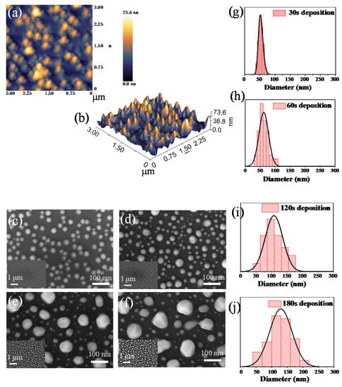
Figure 1.
(a) Atomic force microscope (AFM) top-view of 3 × 3 μm2 of copper nanoparticles; (b) corresponding the 3D image; (c–f) SEM images of copper nanoparticles with different deposition times between 30 and 180 s fabricated at 900 °C; (g–j) corresponding diameter distribution histograms.
The SEM image of copper nanoparticles and the corresponding elemental mappings by EDS are shown in Figure 2. Si, O and Cu were observed in the sample, and the peaks of Si, O, Cu and Pt can be found in the EDS spectra. Since the sample was fabricated directly on the quartz substrate, the measured Si and O contents account for most of the color observed in Figure 2c,d. Before testing, we sputtered Pt with a nanoparticle size of 20 nm on copper nanoparticles to increase the conductivity of the sample and observe nanoparticle topography from charge accumulation at higher magnifications. From Figure 2a to Figure 2b, the amount of copper deposition increased and the proportion of the Cu element increased. It can be seen in Figure 2a that the time of sputtering for copper was less than it was the Figure 2b, and the Cu in Figure 2a accounts for 5.54%. The longer sputtering time evidenced by the proportion of Cu accounts for 9.35%. This also proves that the copper nanoparticles remaining on the substrate increase with increasing deposition time. The blue dots in Figure 2c,d show the magnification of copper nanoparticles, which also corresponds to the SEM image. The island-like distribution is also confirmed by Figure 2c,d’s copper distribution caused by the SSD growth mechanism [41,42].
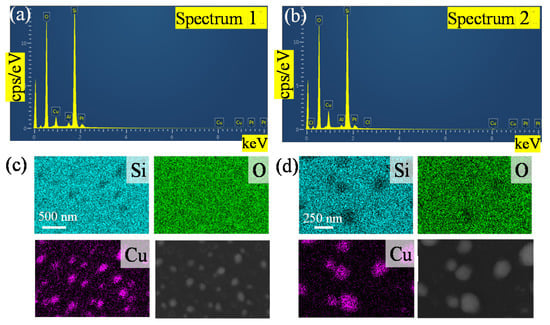
Figure 2.
Energy dispersive X-ray spectroscopy (EDS) elemental characterization of the copper nanoparticles fabricated with the different deposition times at 900 °C; (a,c) the EDS spectra of the copper for a deposition time of 90 s; (b,d) the EDS spectra of the copper for a deposition time of 120 s.
Furthermore, we studied the SEM side-views of copper nanoparticles coated with TiO2. The TiO2 layers were deposited using spin-coating and then annealed at 550 °C under ambient air for 1 h. The schematic illustration of the copper nanoparticles covered with TiO2 can be seen in Figure 3a; it is obvious that the structure is similar to the physical model we expected to build, as shown in Figure 3b–d. The arrows point exactly to the copper nanoparticles and TiO2 films we synthesized, respectively. Thus, we can see that the copper nanoparticles are also island-like when they are covered with oxides, and the oxide coating was made on the copper nanoparticles with layers of about 40 nm in thickness (Figure 3d). Figure 3c,d shows different sizes of copper nanoparticles covered in TiO2 between 119 and 155 nm thick. The presence of oxide can also be seen in the divided areas between the copper nanoparticles, which shows that the uniformity of the film is perfect when spin-coating. The copper nanoparticles are tightly wrapped by the titanium dioxide, which can change the LSPR [1,43] of the metal nanoparticles. After measuring the structure by SEM and AFM, the absorption of the material structure was also investigated to show the absorbance change.
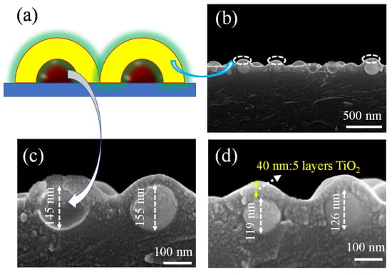
Figure 3.
(a) Schematic illustrations of the Cu/TiO2 composite film: the arrows represent copper nanoparticles and TiO2 films, respectively. (b) SEM side-view of the Cu/TiO2 composite film. (c,d) Enlarged SEM side-views of the Cu nanoparticles covered with TiO2 of varying thickness.
Figure 4a–d shows absorbance evolution by varying TiO2 thickness on copper nanoparticles of different sizes. Absorption spectra as recorded using a CRAIC 20/30 PVTM microspectrophotometer in the wavelengths varying from 200 to 2000 nm (Figure 4a–d) show the absorption spectra of nanoparticles at 200–1400 nm. The surface plasmon resonance band (SPR) [44,45] of the copper nanoparticles varies from 570 nm to 580 nm. The absorption maximum of each sample corresponds to that of the surface plasmon band of the copper nanoparticles. With the increase of copper deposition time, the intensity of the absorption also increases and the absorption of copper nanoparticles has a 10 nm red shift due to the particle size increase with the time of copper deposition. At the same time, the absorption of copper nanoparticles covered by 1-layer or 2-layers TiO2 is also studied in Figure 4. The absorption spectra of different samples exhibited the obvious absorption bands between 670 and 770 nm and 765 and 835 nm originating from the SPR [44,45] of the copper nanoparticles with TiO2, and the absorption spectra of TiO2 appear at 330 nm. It is obvious that the second peak is the absorption of copper nanoparticles covered with TiO2, and the absorption peak of copper nanoparticles whether covered one layer or two layers of TiO2 has an obvious red-shift compared to the absorption of pure copper nanoparticles. The absorption has maximum red shifts of 160 and 235 nm compared to the peak of pure copper nanoparticles appearing at about 600 nm, respectively. The reason for the red shift is mainly due to the size effect of copper nanoparticles [46]. Additionally, the metal nanoparticles significantly increase light absorption and produce a plasmon resonance frequency shift of the absorption peak. In the meantime, the red shift of absorption of copper nanoparticles covered in TiO2 depends on the modulation of dielectric environment [47], and the absorption peak of copper nanoparticles has much more red shift compared to the isolated copper nanoparticles. Thus, the absorption peak position of the nanoparticles reached 835 nm from the original 570 nm. As the same time, it is obvious that the copper deposition time of 150 s covered in two layers of TiO2 has a wider absorption band than the other samples.
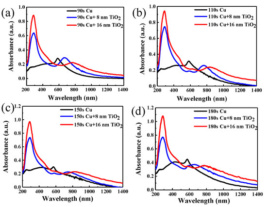
Figure 4.
Absorbance evolution with TiO2 thickness on copper nanoparticles with different deposition times: (a) 90 s, (b) 110 s, (c) 150 s, (d) 180 s.
Figure 5 shows the change of absorbance peak position and absorbance peak position of copper nanoparticles covered by TiO2 of different thickness. As the same time, we can obtain that the absorbance peak has a red shift when the surfaces of copper nanoparticles are covered in one or two layers TiO2. The biggest change of the absorption peak is from the original 580 nm to about 830 nm can be seen in Figure 5a. But the 180 s copper deposition covered 2 layers TiO2 does not perform as well as other samples and the maximum absorption appear at 750 nm. At the same time, the intensity of absorption is also one of important factors in terms of fluorescence enhancement. We can see that the intensity of the absorption peak showing a downward trend in Figure 5b. When the absorption peak position reaches the near infrared band, it must also ensure the absorption intensity. Thus, the time of 90 s, 110 s, 150 s coper deposition covered TiO2 are selected samples to study the enhancement of fluorescence.
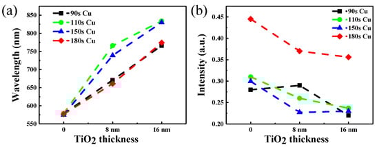
Figure 5.
(a) The change of absorbance peak position of copper nanoparticles covered by TiO2 of different thickness, (b) the change of the peak absorbance position of copper nanoparticles covered by TiO2 of various thicknesses.
In the synthesis of the NaGdF4:Yb3+, Er3+ nanoparticles, we adopted hydrothermal method. When the heating temperature was selected, the operation was carried out by heating between zones while maintaining a certain temperature for half an hour to keep the size of NaGdF4:Yb3+, Er3+ nanoparticles uniform. As the same time, the size is typically ~9 nm in the TEM image and the size distribution can be seen in Figure 6a,b. The particles size varies from 6 to 12 nm and it fits to the normal distribution. Figure 6c shows the XRD patterns NaGdF4:Yb3+, Er3+ nanoparticles. The diffraction peaks in Figure 6c at 29.6°, 42.7°, 53.4° match well with XRD peaks of the standard cards (JCPDS:27-0699) of NaGdF4:Yb3+, Er3+ because of X-ray diffraction of the (1 0 1), (2 0 1) and (2 1 1) facets [48]. The spectrum of the measured sample is consistent with the standard card, indicating that the material formed a certain lattice structure which can be seen in Figure 6a. The up-conversion material was also spin-coated on top of the copper nanoparticles and then the basic fluorescence test was performed after a simple curing process by drying at room temperature.
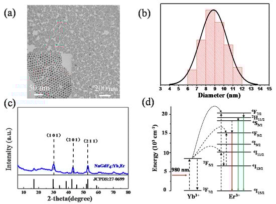
Figure 6.
(a) TEM image of NaGdF4:Yb, Er nanoparticles; (b) corresponding diameter distribution histogram; (c) XRD pattern of NaGdF4:Yb, Er; (d) the mechanism of up-conversion processes of NaGdF4:Yb, Er.
The NaGdF4 can be known as the popular material for up-conversion luminescence and under 980 nm excitation [9], NaGdF4 can have green and red emission doping Yb3+, Er3+. Figure 6d is the mechanism of up-conversion processes of NaGdF4:Yb3+, Er3+, Yb3+ absorbs the energy of the 980 nm which the energy can transfers into Er3+ and Er3+ return to ground state from excited state [49]. Energy level schematic can be explained by the following theory. First, the electrons of Yb ions can change from 2F7/2 to 2F5/2 under the laser of 980 nm, which can influence the electrons of Er ions from 4I15/2 to 4I11/2 [35]. As the same time, a part of electrons changes from 4I11/2 to 4I13/2 by the non-radiative method on the surface of up-conversion nanoparticles. Then adjacent Yb ions can absorb electrons and influence the Er ions which can change the energy state of Er ions from 4I11/2 to 4F7/2 or from 4I13/2 to 4F9/2. And on the 4F7/2 energy level of Er ions to 2H11/2 and 4S3/2 by the method of non-radiative which can cause the green emission of 2H11/2→4I15/2 and 4S3/2→4I15/2. As the same time, on the 4F9/2 energy level of Er ions can radiate to the ground state which generate 4F9/2→4I15/2 transitions [36,50]. Thus, the green emission from 515 nm to 530 nm and 530 nm to 550 nm is determined by 2H11/2→4I15/2 and 4S3/2→4I15/2 transitions. The red emission is attributed to the 4F9/2→4I15/2 transitions. Here in this work, the 542 nm and 660 nm emission are our targeted.
During the fluorescence test, we selected samples of copper nanoparticles at different deposition times of 2-layer TiO2, and also performed a bare control. There are two obvious fluorescence emission peaks of the NaGdF4:Yb, Er nanoparticles: green emission at 542 nm and red emission at 660 nm in Figure 7a. The intensity of fluorescence measured directly on quartz glass is weak as the amount of up-conversion material left on the glass sheet by spin coating is very low, and there is a dramatic enhancement observed in the measured fluorescence when the up-conversion material spin-coating on the Cu/TiO2 structure. This also illustrates that the localized surface plasmon resonance (LSPR) peak plays a role in luminescence enhancement of up-conversion nanoparticles. The SPR of the Cu/TiO2 red shifted to 835 nm, matching well with the excitation wavelength, as can be seen in Figure 4. The ratio of different fluorescence emission is recorded in Figure 7b. It can be seen that as the time of copper deposition covered TiO2 increases, the maximum fluorescence ration overall increases gradually. Thus, with the LSPR peak is turned to 835 nm, the ratios of green and red emission can be about 3 and 2 times, respectively. The results show the LSPR with the excitation field can influence the up-conversion luminescence and then cause a strength enhancement of the local excitation field [35].
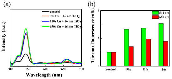
Figure 7.
(a) Fluorescence spectra of NaGdF4:Yb, Er on the Cu/TiO2 composite film. (b) Histograms of the maximum fluorescence intensity ratio between 542 nm and 660 nm emission.
4. Conclusions
In this work, the Cu/TiO2 hybrid film was successfully synthesized which the copper nanoparticles prepared by sputtering and the TiO2 film used by spin-coating. The evolutions of the morphological and optical properties of copper nanoparticles and TiO2 were studied. We concluded that the maximum absorption of the Cu/TiO2 hybrid film appeared at about 835 nm, and it redshift about 235 nm more than the absorption of pure copper nanoparticles. The changing of absorption is mainly related to the different thickness of TiO2 on the copper nanoparticles. As the same time, the position of the maximum absorbance of hybrid film matches with the excitation of the up-conversion. Thus, the fluorescence of up-conversion material enhanced and the maximum ratios of intensity of fluorescence at 542 nm and 650 nm were 3.1 and 1.9, respectively. The enhanced fluorescence was related to the surface plasmon which was mainly from the excitation field enhancement due to the modulation of dielectric environment by changing the TiO2 layer’s thickness. Because of this simple and feasible way to enhance the up-conversion fluorescence, the fabrication of Cu/TiO2 film is expected to be used in bioprobes for optical tracking, solar cells effective for absorbed infrared light and anti-counterfeiting technology.
Author Contributions
Conceptualization and supervision, J.T. and L.A.B.; methodology, Y.P.; writing—original draft preparation, Y.P. and B.L.; writing—review and editing, L.C. and J.L.; funding acquisition, J.T. and L.A.B. All authors have read and agreed to the published version of the manuscript.
Funding
This work was supported by (1) State Key Project of International Cooperation Research (2017YFE0108300, 2016YFE0110800); (2) National Natural Science Foundation of China (51473082); (3) The Program for Introducing Talents of Discipline to Universities (“111” plan); (4) The Double Hundred Foreign Expert Project of Shandong Province; (5) 1st Class Discipline Program of Materials Science of Shandong Province, China.
Conflicts of Interest
The authors declare no conflict of interest.
References
- Fang, Z.; Zhen, Y.-R.; Fan, L.; Zhu, X.; Nordlander, P. Tunable wide-angle plasmonic perfect absorber at visible frequencies. Phys. Rev. B 2012, 85, 1–7. [Google Scholar] [CrossRef]
- Lu, C.Y.; Browne, D.E.; Yang, T.; Pan, J.W. Demonstration of a compiled version of Shor’s quantum factoring algorithm using photonic qubits. Phys. Rev. Lett. 2007, 99, 250504. [Google Scholar] [CrossRef] [PubMed]
- Zhang, Y.; Aslan, K.; Previte, M.J.R.; Geddes, C.D. Metal-enhanced fluorescence from copper substrates. Appl. Phys. Lett. 2007, 90, 1–3. [Google Scholar] [CrossRef]
- Jing, Z.; Zhuang, L.; Li, F. Upconversion Nanophosphors for Small-Animal Imaging. Chem. Soc. Rev. 2012, 41, 1323–1349. [Google Scholar] [CrossRef]
- Jiao, J.; Li, Y.; Shen, W.; Gai, S.; Tang, J.; Wang, Y.; Huang, L.; Liu, J.; Wang, W.; Belfiore, L.A. Fabrication and luminescence of KGdF4:Yb3+/Er3+ nanoplates and their improving performance for polymer solar cells. Sci. Bull. 2018, 63, 216–218. [Google Scholar] [CrossRef]
- Deng, R.; Qin, F.; Chen, R.; Huang, W.; Hong, M.; Liu, X. Temporal full-colour tuning through non-steady-state upconversion. Nat. Nanotechnol. 2015, 10, 237–242. [Google Scholar] [CrossRef]
- Zhang, Y.; Zhang, L.; Deng, R.; Tian, J.; Zong, Y.; Jin, D.; Liu, X. Multicolor Barcoding in a Single Upconversion Crystal. J. Am. Chem. Soc. 2014, 136, 4893–4896. [Google Scholar] [CrossRef]
- Haase, P.D.M.; Schfer, D.H. Upconverting Nanoparticles. Angew. Chem. Int. Ed. 2011, 50, 5808–5829. [Google Scholar] [CrossRef]
- Li, Y.; Jiao, J.; Yan, P.; Liu, L.; Wang, J.; Wang, Y.; Huang, L.; Liu, J.; Belfiore, L.A.; Tang, J. Synthesis and tunable photoresponse for core-shell structured NaGdF4: Yb, Er@SiO2@Eu(TTA)3Phen nanocomplexes. Scr. Mater. 2018, 152, 1–5. [Google Scholar] [CrossRef]
- Guo, H.; Li, Z.; Qian, H.; Hu, Y.; Niagara Muhammad, I. Seed-mediated synthesis of NaYF4:Yb, Er/NaGdF4 nanocrystals with improved upconversion fluorescence and MR relaxivity. Nanotechnology 2010, 21, 125602. [Google Scholar] [CrossRef]
- Liu, F.Y.; He, X.X.; Liu, L.; You, H.P.; Zhang, H.M.; Wang, Z.X. Conjugation of NaGdF4 upconverting nanoparticles on silica nanospheres as contrast agents for multi-modality imaging. Biomaterials 2013, 34, 5218–5225. [Google Scholar] [CrossRef] [PubMed]
- Chen, G.; Ohulchanskyy, T.Y.; Law, W.C.; Ågren, H.; Prasad, P.N. Monodisperse NaYbF4:Tm3+/NaGdF4 core/shell nanocrystals with near-infrared to near-infrared up-conversion photoluminescence and magnetic resonance properties. Nanoscale 2011, 3, 2003–2008. [Google Scholar] [CrossRef] [PubMed]
- Chung, W.J.; Yoo, J.R.; Kim, Y.S.; Heo, J. Mechanism of the blue up-conversion in Tm3+/Nd3+-doped calcium aluminate glasses. J. Am. Ceram. Soc. 2010, 80, 1485–1490. [Google Scholar] [CrossRef]
- Ren, G.; Zeng, S.; Hao, J. Tunable Multicolor Upconversion Emissions and Paramagnetic Property of Monodispersed Bifunctional Lanthanide-Doped NaGdF4 Nanorods. J. Phys. Chem. C 2011, 115, 20141–20147. [Google Scholar] [CrossRef]
- Li, H.; Deng, Q.; Liu, B.; Yang, J.; Wu, B. Fabrication of core@spacer@shell Aunanorod@mSiO2@Y2O3: Er nanocomposites with enhanced upconversion fluorescence. RSC Adv. 2016, 6, 13343–13348. [Google Scholar] [CrossRef]
- Cheng, Y.; Sun, K. Enhanced Up-Conversion Emission in Al3+ Co-Doped ZnGa2O4:Yb3+, Tm3+ Powder Phosphors. J. Fluoresc. 2018, 28, 801–808. [Google Scholar] [CrossRef]
- Wu, X.; Yin, S.; Dong, Q.; Liu, B.; Wang, Y.; Sekino, T.; Lee, S.W.; Sato, T. UV, visible and near-infrared lights induced NOx destruction activity of (Yb, Er)-NaYF4/C-TiO2 composite. Sci. Rep. 2013, 3, 2918. [Google Scholar] [CrossRef]
- Zhang, F.; Wan, Y.; Yu, T.; Zhang, F.; Shi, Y.; Xie, S.; Li, Y.; Xu, L.; Tu, B.; Zhao, D. Uniform nanostructured arrays of sodium rare-earth fluorides for highly efficient multicolor upconversion luminescence. Angew. Chem. Int. Ed. 2007, 46, 7976–7979. [Google Scholar] [CrossRef]
- Avnir, D.; Kaufman, V.R.; Reisfeld, R. Organic fluorescent dyes trapped in silica and silica-titania thin films by the sol-gel method. Photophysical, film and cage properties. J. Non Cryst. Solids 1985, 74, 395–406. [Google Scholar] [CrossRef]
- Resch-Genger, U.; Grabolle, M.; Cavaliere-Jaricot, S.; Nitschke, R.; Nann, T. Quantum dots versus organic dyes as fluorescent labels. Nat. Methods 2008, 5, 763–775. [Google Scholar] [CrossRef]
- Wilson, L.R.; Richards, B.S. Measurement method for photoluminescent quantum yields of fluorescent organic dyes in polymethyl methacrylate for luminescent solar concentrators. Appl. Opt. 2009, 48, 212–220. [Google Scholar] [CrossRef] [PubMed]
- Reiss, P.; Protière, M.; Li, L. Core/Shell Semiconductor Nanocrystals. Small 2009, 5, 154–168. [Google Scholar] [CrossRef] [PubMed]
- Bruchez, M.P. Semiconductor Nanocrystals as Fluorescent Biological Labels. Science 1998, 281, 2013–2016. [Google Scholar] [CrossRef] [PubMed]
- Macdougall, S.K.W.; Ivaturi, A.; Marques-Hueso, J.; Krämer, K.W.; Richards, B.S. Ultra-high photoluminescent quantum yield of β-NaYF4: 10% Er3+ via broadband excitation of upconversion for photovoltaic devices. Opt. Express 2012, 20, A879. [Google Scholar] [CrossRef] [PubMed]
- Liedberg, B.; Lundström, I.; Stenberg, E. Principles of biosensing with an extended coupling matrix and surface plasmon resonance. Sens. Actuators, B 1993, 11, 63–72. [Google Scholar] [CrossRef]
- Hutter, E.; Fendler, J.H. Exploitation of Localized Surface Plasmon Resonance. Adv. Mater. 2004, 16, 1685–1706. [Google Scholar] [CrossRef]
- Arppe, R.; Sørensen, T.J. Physical unclonable functions generated through chemical methods for anti-counterfeiting. Nat. Rev. Chem. 2017, 1, 0031. [Google Scholar] [CrossRef]
- Barnes, W.L.; Dereux, A.; Ebbesen, T.W. Surface plasmon subwavelength optics. Nature. 2003, 424, 824–830. [Google Scholar] [CrossRef]
- Homola, J.; Yee, S.S.; Gauglitz, G. Surface Plasmon Resonance Sensors: Review. Anal. Bioanal. Chem. 1999, 377, 528–539. [Google Scholar] [CrossRef]
- Homola, J. Present and future of surface plasmon resonance biosensors. Anal. Bioanal. Chem. 2003, 377, 528–539. [Google Scholar] [CrossRef]
- Futamata, M.; Maruyama, Y.; Ishikawa, M. Local Electric Field and Scattering Cross Section of Ag Nanoparticles under Surface Plasmon Resonance by Finite Difference Time Domain Method. J. Phys. Chem. B 2003, 107, 7607–7617. [Google Scholar] [CrossRef]
- Suyver, J.F.; Aebischer, A.; Biner, D.; Gerner, P.; Grimm, J.; Heer, S.; Krämer, K.W.; Reinhard, C.; Güdel, H.U. Novel materials doped with trivalent lanthanides and transition metal ions showing near-infrared to visible photon upconversion. Opt. Mater. 2005, 27, 1111–1130. [Google Scholar] [CrossRef]
- Hong, Y.P.; Dwight, K. Crystal structure and fluorescence lifetime of a laser material NdNa5(WO4)4. Mater. Res. Bull. 1974, 9, 775–780. [Google Scholar] [CrossRef]
- Manurung, R.V.; Wu, C.T.; Roy, P.K.; Chattopadhyay, S. A plasmon-tuned ‘gold sandwich’ for metal enhanced fluorescence in silica coated NaYF4:Yb,Er upconversion nanoparticles. RSC Adv. 2016, 6, 87088–87095. [Google Scholar] [CrossRef]
- Chen, X.; Zhou, D.; Xu, W.; Zhu, J.; Pan, G.; Yin, Z.; Wang, H.; Zhu, Y.; Shaobo, C.; Song, H. Fabrication of Au-Ag nanocage@NaYF4@NaYF4:Yb,Er Core-Shell Hybrid and its Tunable Upconversion Enhancement. Sci. Rep. 2017, 7, 41079. [Google Scholar] [CrossRef]
- Wang, H.; Li, M.; Yin, Z.; Zhang, T.; Chen, X.; Zhou, D.; Zhu, J.; Xu, W.; Cui, H.; Song, H. Remarkable Enhancement of Upconversion Luminescence on Cap-Ag/PMMA Ordered Platform and Trademark Anticounterfeiting. ACS Appl. Mater. Interfaces 2017, 9, 37128–37135. [Google Scholar] [CrossRef]
- Sui, M.; Zhang, Q.; Kunwar, S.; Pandey, P.; Li, M.-Y.; Lee, J. Study on the dimensional, configurational and optical evolution of palladium nanostructures on c-plane sapphire by the control of annealing temperature and duration. Appl. Surf. Sci. 2017, 416, 1–13. [Google Scholar] [CrossRef]
- Thompson, C.V. Solid-State Dewetting of Thin Films. Annu. Rev. Mater. Res. 2012, 42, 399–434. [Google Scholar] [CrossRef]
- Zhao, X.; Lee, U.-J.; Lee, K.-H. Dewetting behavior of Au films on porous substrates. Thin Solid Films 2010, 519, 706–713. [Google Scholar] [CrossRef]
- Pandey, P.; Sui, M.; Zhang, Q.; Li, M.-Y.; Kunwar, S.; Lee, J. Systematic control of the size, density and configuration of Pt nanostructures on sapphire (0 0 0 1) by the variation of deposition amount and dwelling time. Appl. Surf. Sci. 2016, 368, 198–207. [Google Scholar] [CrossRef]
- Yao, J.H.; Elder, K.R.; Guo, H.; Grant, M. Theory and simulation of Ostwald ripening. Phys. Rev. B 1993, 47, 14110–14125. [Google Scholar] [CrossRef] [PubMed]
- Marqusee, J.A.; Ross, J. Theory of Ostwald ripening: Competitive growth and its dependence on volume fraction. J. Chem. Phys. 1984, 80, 536–543. [Google Scholar] [CrossRef]
- Zhan, Q.; Zhang, X.; Zhao, Y.; Liu, J.; He, S. Tens of thousands-fold upconversion luminescence enhancement induced by a single gold nanorod. Laser Photonics Rev. 2015, 9, 479–487. [Google Scholar] [CrossRef]
- Chen, H.; Shao, L.; Li, Q.; Wang, J. Gold nanorods and their plasmonic properties. Chem. Soc. Rev. 2013, 42, 2679–2724. [Google Scholar] [CrossRef] [PubMed]
- Ruan, Q.; Shao, L.; Shu, Y.; Wang, J.; Wu, H. Growth of Monodisperse Gold Nanospheres with Diameters from 20 nm to 220 nm and Their Core/Satellite Nanostructures. Adv. Opt. Mater. 2014, 2, 65–73. [Google Scholar] [CrossRef]
- Rostovshchikova, T.N.; Smirnov, V.V.; Kozhevin, V.M.; Yavsin, D.A.; Zabelin, M.A.; Yassievich, I.N.; Gurevich, S.A. New size effect in the catalysis by interacting copper nanoparticles. Appl. Catal. A 2005, 296, 70–79. [Google Scholar] [CrossRef]
- Mao, S.; Liu, J.; Pan, Y.; Lee, J.; Yao, Z.; Pandey, P.; Kunwar, S.; Zhu, Z.; Shen, W.; Belfiore, L.A.; et al. Morphological and optical evolution of metallic oxide/Au nanoparticle hybrid thin film: High absorption and reflectance by plasmonic enhancement. Appl. Surf. Sci. 2019, 495, 143575. [Google Scholar] [CrossRef]
- Lv, B.; Jiao, J.; Liu, Y.; Liu, L.; Zhang, J.; Li, Y.; Wang, J.; Tang, J. Heterostructure NaGdF4:Yb,Er anchored on MIL-101 for promoting photoelectronic response and photocatalytic activity. Nanoscale 2019, 11, 22730–22733. [Google Scholar] [CrossRef]
- Liang, Z.; Sun, E.; Liu, Z.; Zhang, Z.; Zeng, J.; Ruan, W.; Li, G.; Cao, W. Electric field induced upconversion fluorescence enhancement and its mechanism in Er3+ doped 0.75Pb(Mg1/3Nb2/3)O3-0.25PbTiO3 transparent ceramic. Appl. Phys. Lett. 2016, 109, 132904. [Google Scholar] [CrossRef]
- Maurya, S.K.; Tiwari, S.P.; Kumar, A.; Kumar, K. Plasmonic enhancement of upconversion emission in Ag@NaYF4:Er3+/Yb3+ phosphor. J. Rare Earths 2018, 36, 903–910. [Google Scholar] [CrossRef]


© 2020 by the authors. Licensee MDPI, Basel, Switzerland. This article is an open access article distributed under the terms and conditions of the Creative Commons Attribution (CC BY) license (http://creativecommons.org/licenses/by/4.0/).