Tuning the Morphology and Properties of Nanostructured Cu-ZnO Thin Films Using a Two-Step Sputtering Technique


Abstract
1. Introduction
2. Materials and Methods
3. Results and Discussion
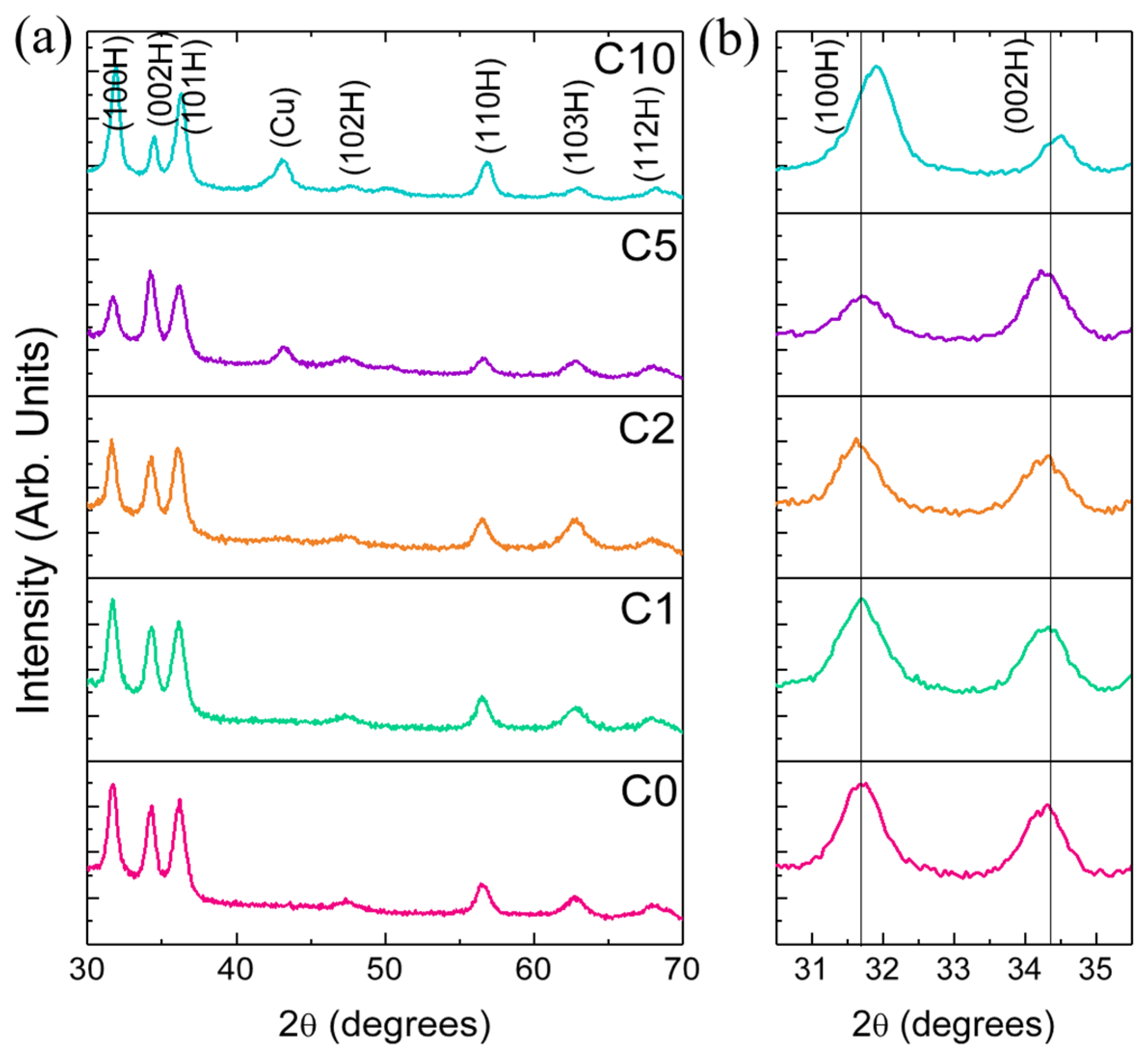
3.1. XRD Analysis
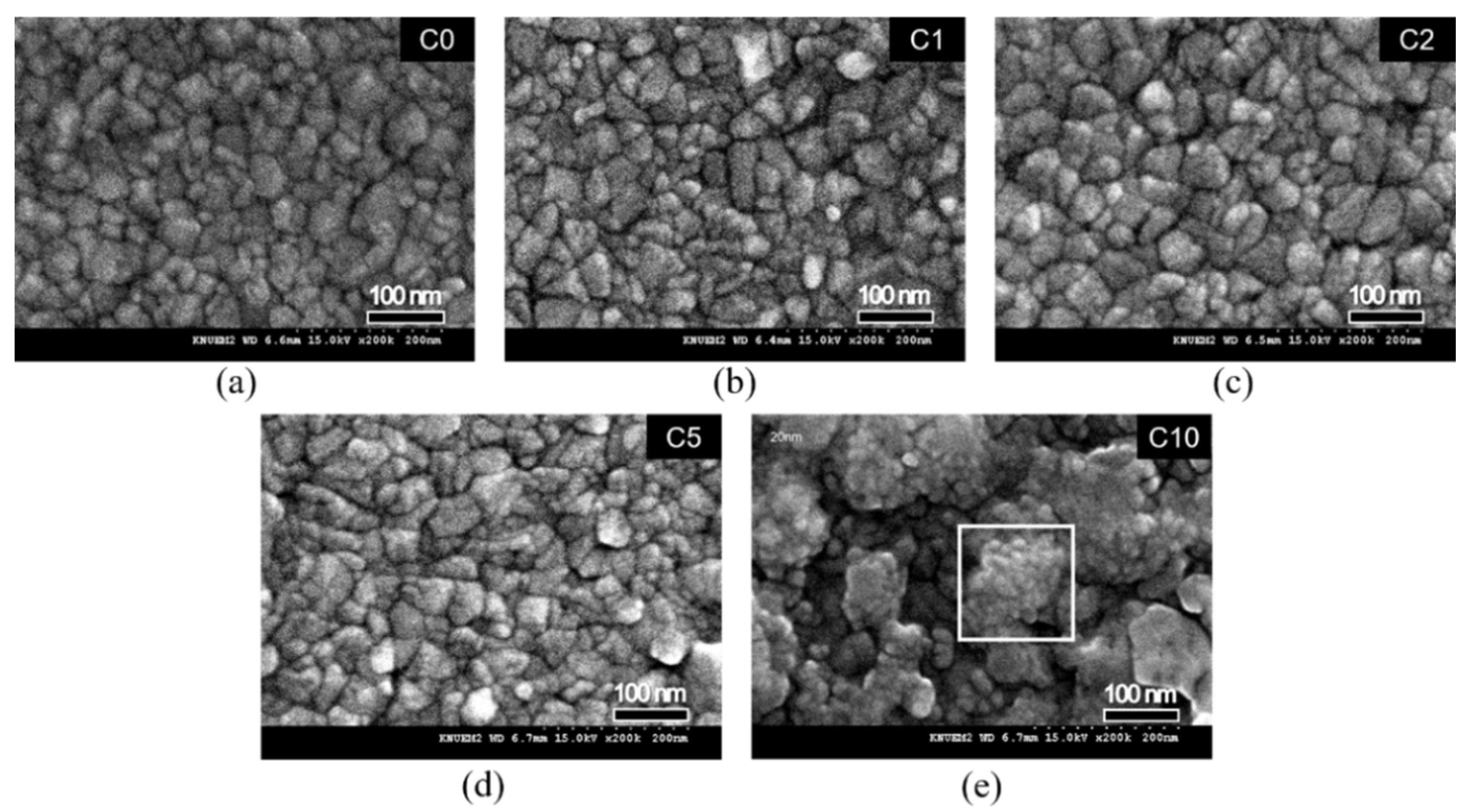
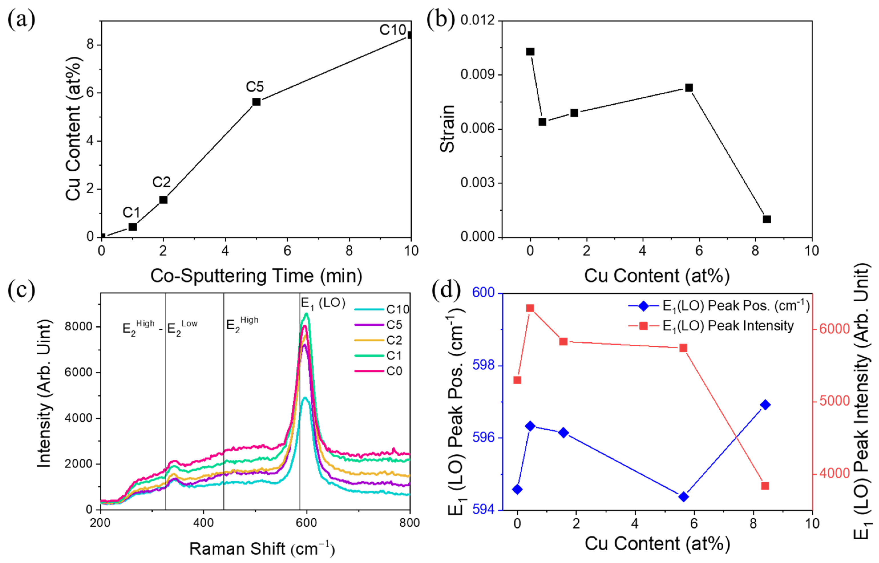
3.2. SEM/EDX Analysis
3.3. Williamson-Hall Analysis
3.4. Raman Analysis
3.5. UV-Vis Analysis
3.6. Electrical Conductivity Analysis
3.7. Crystal Growth Mechanism
4. Conclusions
Supplementary Materials
Author Contributions
Funding
Acknowledgments
Conflicts of Interest
References
- Tan, S.T.; Sun, X.W.; Zhang, X.H.; Chua, S.J.; Chen, B.J.; Teo, C.C. Cluster coarsening in zinc oxide thin films by postgrowth annealing. J. Appl. Phys. 2006, 100, 033502. [Google Scholar] [CrossRef]
- Chen, M.; Pei, Z.L.; Sun, C.; Wen, L.S.; Wang, X. Formation of Al-doped ZnO films by dc magnetron reactive sputtering. Mater. Lett. 2001, 48, 194–198. [Google Scholar] [CrossRef]
- Özgür, Ü.; Alivov, Y.I.; Liu, C.; Teke, A.; Reshchikov, M.A.; Doǧan, S.; Avrutin, V.; Cho, S.J.; Morko̧, H. A comprehensive review of ZnO materials and devices. J. Appl. Phys. 2005, 98, 11. [Google Scholar] [CrossRef]
- Gupta, K.M.; Gupta, N. Recent Advances in Semiconducting Materials and Devices; Springer: Cham, Switzerland, 2015; Volume 80, pp. 531–562. [Google Scholar]
- Chen, J.J.; Gao, Y.; Zeng, F.; Li, D.M.; Pan, F. Effect of sputtering oxygen partial pressures on structure and physical properties of high resistivity ZnO films. Appl. Surf. Sci. 2004, 223, 318–329. [Google Scholar] [CrossRef]
- Blom, F.R.; van de Pol, F.C.M.; Bauhuis, G.; Popma, T.J.A. RF planar magnetron sputtered ZnO films II: Electrical properties. Thin Solid Films 1991, 204, 365–376. [Google Scholar] [CrossRef]
- Zhou, L.; Huang, Z.; Zhao, X.; He, Y.; Chen, L.; Xu, M.; Zhao, K.; Zhang, S.; Ouyang, X. A High-Resistivity ZnO Film-Based Photoconductive X-Ray Detector. IEEE Photonics Technol. Lett. 2019, 31, 365–368. [Google Scholar] [CrossRef]
- Zhao, X.; Chen, L.; He, Y.; Liu, J.; Peng, W.; Huang, Z.; Qi, X.; Pan, Z.; Zhang, W.; Zhang, Z.; et al. Nanosecond X-ray detector based on high resistivity ZnO single crystal semiconductor. Appl. Phys. Lett. 2016, 108, 171103. [Google Scholar] [CrossRef]
- Ellmer, K. Resistivity of polycrystalline zinc oxide films: Current status and physical limit. J. Phys. D. Appl. Phys. 2001, 34, 3097–3108. [Google Scholar] [CrossRef]
- Jeong, J.A.; Choi, K.H.; Bae, J.H.; Moon, J.M.; Jeong, S.W.; Kim, I.; Kim, H.K.; Yi, M.S. Electrical, optical, and structural properties of ITO co-sputtered IZO films by dual target magnetron sputtering. J. Electroceramics 2009, 23, 361–366. [Google Scholar] [CrossRef]
- Kim, Y.S.; Tai, W.P. Electrical and optical properties of Al-doped ZnO thin films by sol-gel process. Appl. Surf. Sci. 2007, 253, 4911–4916. [Google Scholar] [CrossRef]
- Bundesmann, C.; Ashkenov, N.; Schubert, M.; Spemann, D.; Butz, T.; Kaidashev, E.M.; Lorenz, M.; Grundmann, M. Raman scattering in ZnO thin films doped with Fe, Sb, Al, Ga, and Li. Appl. Phys. Lett. 2003, 83, 1974–1976. [Google Scholar] [CrossRef]
- Meza, D.; Cruz, A.; Morales-Vilches, A.B.; Korte, L.; Stannowski, B. Aluminum-doped zinc oxide as front electrode for rear emitter silicon heterojunction solar cells with high efficiency. Appl. Sci. 2019, 9, 862. [Google Scholar] [CrossRef]
- Ji, X.; Song, J.; Wu, T.; Tian, Y.; Han, B.; Liu, X.; Wang, H.; Gui, Y.; Ding, Y.; Wang, Y. Solar Energy Materials and Solar Cells Fabrication of high-performance F and Al co-doped ZnO transparent conductive fi lms for use in perovskite solar cells. Sol. Energy Mater. Sol. Cells 2019, 190, 6–11. [Google Scholar] [CrossRef]
- Zhang, H.W.; Wei, Z.R.; Li, Z.Q.; Dong, G.Y. Room-temperature ferromagnetism in Fe-doped, Fe- and Cu-codoped ZnO diluted magnetic semiconductor. Mater. Lett. 2007, 61, 3605–3607. [Google Scholar] [CrossRef]
- Yang, L.W.; Wu, X.L.; Huang, G.S.; Qiu, T.; Yang, Y.M. In situ synthesis of Mn-doped ZnO multileg nanostructures and Mn-related Raman vibration. J. Appl. Phys. 2005, 97, 1–4. [Google Scholar] [CrossRef]
- Loeza-Poot, M.; Mis-Fernández, R.; Rimmaudo, I.; Camacho-Espinosa, E.; Peña, J.L. Novel sputtering method to obtain wide band gap and low resistivity in as-deposited magnesium doped zinc oxide films. Mater. Sci. Semicond. Process. 2019, 104, 104646. [Google Scholar] [CrossRef]
- Chen, H.; Du Pasquier, A.; Saraf, G.; Zhong, J.; Lu, Y. Dye-sensitized solar cells using ZnO nanotips and Ga-doped ZnO films. Semicond. Sci. Technol. 2008, 23, 045004. [Google Scholar] [CrossRef]
- Wang, X.B.; Song, C.; Geng, K.W.; Zeng, F.; Pan, F. Photoluminescence and Raman scattering of Cu-doped ZnO films prepared by magnetron sputtering. Appl. Surf. Sci. 2007, 253, 6905–6909. [Google Scholar] [CrossRef]
- Al-Khanbashi, H.A.; Shirbeeny, W.; Al-Ghamdi, A.A.; Bronstein, L.M.; Mahmoud, W.E. Development of highly conductive and transparent copper doped zinc oxide thin films via 2-methoxyethanol modified sol-gel dip-coating technique. Ceram. Int. 2014, 40, 1927–1932. [Google Scholar] [CrossRef]
- Ma, L.; Ma, S.; Chen, H.; Ai, X.; Huang, X. Microstructures and optical properties of Cu-doped ZnO films prepared by radio frequency reactive magnetron sputtering. Appl. Surf. Sci. 2011, 257, 10036–10041. [Google Scholar] [CrossRef]
- Peng, X.; Xu, J.; Zang, H.; Wang, B.; Wang, Z. Structural and PL properties of Cu-doped ZnO films. J. Lumin. 2008, 128, 297–300. [Google Scholar] [CrossRef]
- Agarwal, D.C.; Singh, U.B.; Gupta, S.; Singhal, R.; Kulriya, P.K.; Singh, F.; Tripathi, A.; Singh, J.; Joshi, U.S.; Avasthi, D.K. Enhanced room temperature ferromagnetism and green photoluminescence in Cu doped ZnO thin film synthesised by neutral beam sputtering. Sci. Rep. 2019, 9, 1–12. [Google Scholar] [CrossRef] [PubMed]
- Sudakar, C.; Thakur, J.S.; Lawes, G.; Naik, R.; Naik, V.M. Ferromagnetism induced by planar nanoscale CuO inclusions in Cu-doped ZnO thin films. Phys. Rev. B Condens. Matter Mater. Phys. 2007, 75, 1–6. [Google Scholar] [CrossRef]
- Liu, Y.; Liu, H.; Yu, Y.; Wang, Q.; Li, Y.; Wang, Z. Structural and optical properties of ZnO thin films with heavy Cu-doping prepared by magnetron co-sputtering. Mater. Lett. 2015, 143, 319–321. [Google Scholar] [CrossRef]
- Jilani, A.; Othman, M.H.D.; Ansari, M.O.; Oves, M.; Hussain, S.Z.; Khan, I.U.; Abdel-wahab, M.S. Structural and optical characteristics, and bacterial decolonization studies on non-reactive RF sputtered Cu–ZnO@ graphene based nanoparticles thin films. J. Mater. Sci. 2019, 54, 6515–6529. [Google Scholar] [CrossRef]
- Sung, N.E.; Kang, S.W.; Shin, H.J.; Lee, H.K.; Lee, I.J. Cu doping effects on the electronic and optical properties of Cu-doped ZnO thin films fabricated by radio frequency sputtering. Thin Solid Films 2013, 547, 285–288. [Google Scholar] [CrossRef]
- Sreedhar, A.; Kwon, J.H.; Yi, J.; Kim, J.S.; Gwag, J.S. Enhanced photoluminescence properties of Cu-doped ZnO thin films deposited by simultaneous RF and DC magnetron sputtering. Mater. Sci. Semicond. Process. 2016, 49, 8–14. [Google Scholar] [CrossRef]
- Abd, H. 3D hyperbranched heterostructures of Ag nanocrystals-decorated ZnO nanopillars: Controlled growth and characterization of the optical properties. CrystEngComm 2017, 19, 5591–5603. [Google Scholar]
- Jagtap, R.M.; Kshirsagar, D.R.; Khire, V.H.; Pardeshi, S.K. Facile fabrication of porous La doped ZnO granular nanocrystallites and their catalytic evaluation towards thermal decomposition of ammonium perchlorate. J. Solid State Chem. 2019, 276, 194–204. [Google Scholar] [CrossRef]
- Wang, Y.P.; Lu, J.G.; Bie, X.; Ye, Z.Z.; Li, X.; Song, D.; Zhao, X.Y.; Ye, W.Y. Transparent conductive and near-infrared reflective Cu-based Al-doped ZnO multilayer films grown by magnetron sputtering at room temperature. Appl. Surf. Sci. 2011, 257, 5966–5971. [Google Scholar] [CrossRef]
- Prabhu, Y.; Rao, K.; Kumar, V.; Kumari, B. X-Ray Analysis by Williamson-Hall and Size-Strain Plot Methods of ZnO Nanoparticles with Fuel Variation. World J. Nano Sci. Eng. 2014, 4, 21–28. [Google Scholar] [CrossRef]
- Thandavan, T.M.K.; Gani, S.M.A.; Wong, C.S.; Nor, R.M. Evaluation of Williamson–Hall Strain and Stress Distribution in ZnO Nanowires Prepared Using Aliphatic Alcohol. J. Nondestruct. Eval. 2015, 34, 1–9. [Google Scholar] [CrossRef]
- Dobrozhan, O.; Opanasyuk, A.; Kolesnyk, M.; Demydenko, M.; Cheong, H. Substructural investigations, Raman, and FTIR spectroscopies of nanocrystalline ZnO films deposited by pulsed spray pyrolysis. Phys. Status Solidi Appl. Mater. Sci. 2015, 212, 2915–2921. [Google Scholar] [CrossRef]
- Šćepanović, M.; Grujić-Brojčin, M.; Vojisavljević, K.; Bernikc, S.; Srećković, T. Raman study of structural disorder in ZnO nanopowders. J. Raman Spectrosc. 2010, 41, 914–921. [Google Scholar] [CrossRef]
- Bergman, L.; Chen, X.B.; Huso, J.; Morrison, J.L.; Hoeck, H. Raman scattering of polar modes of ZnO crystallites. J. Appl. Phys. 2005, 98, 4–7. [Google Scholar] [CrossRef]
- Alim, K.A.; Fonoberov, V.A.; Shamsa, M.; Balandin, A.A. Micro-Raman investigation of optical phonons in ZnO nanocrystals. J. Appl. Phys. 2005, 97, 124313. [Google Scholar] [CrossRef]
- Das, J.; Pradhan, S.K.; Sahu, D.R.; Mishra, D.K.; Sarangi, S.N.; Nayak, B.B.; Verma, S.; Roul, B.K. Micro-Raman and XPS studies of pure ZnO ceramics. Phys. B Condens. Matter 2010, 405, 2492–2497. [Google Scholar] [CrossRef]
- Xu, X.L.; Lau, S.P.; Chen, J.S.; Chen, G.Y.; Tay, B.K. Polycrystalline ZnO thin films on Si (1 0 0) deposited by filtered cathodic vacuum arc. J. Cryst. Growth 2001, 223, 201–205. [Google Scholar] [CrossRef]
- Exarhos, G.J.; Sharma, S.K. Influence of processing variables on the structure and properties of ZnO films. Thin Solid Films 1995, 270, 27–32. [Google Scholar] [CrossRef]
- Hassanien, A.S.; Akl, A.A. Influence of composition on optical and dispersion parameters of thermally evaporated non-crystalline Cd50S50-xSex thin films. J. Alloys Compd. 2015, 648, 280–290. [Google Scholar] [CrossRef]
- Srinivasulu, T.; Saritha, K.; Reddy, K.T.R. Synthesis and characterization of Fe-doped ZnO thin films deposited by chemical spray pyrolysis. Mod. Electron. Mater. 2017, 3, 76–85. [Google Scholar] [CrossRef]
- Lim, Y.F.; Chua, C.S.; Lee, C.J.J.; Chi, D. Sol-gel deposited Cu2O and CuO thin films for photocatalytic water splitting. Phys. Chem. Chem. Phys. 2014, 16, 25928–25934. [Google Scholar] [CrossRef] [PubMed]
- Xu, C.X.; Sun, X.W.; Zhang, X.H.; Ke, L.; Chua, S.J. Photoluminescent properties of copper-doped zinc oxide nanowires. Nanotechnology 2004, 15, 856–861. [Google Scholar] [CrossRef]
- Dietz, R.E.; Kamimura, H.; Sturge, M.D.; Yariv, A. Electronic structure of copper impurities in ZnO. Phys. Rev. 1963, 132, 1559–1569. [Google Scholar] [CrossRef]
- Huang, P.S.; Qin, F.; Lee, J.K. Role of the Interface between Ag and ZnO in the Electric Conductivity of Ag Nanoparticle-Embedded ZnO. ACS Appl. Mater. Interfaces 2020, 12, 4715–4721. [Google Scholar] [CrossRef]


| Samples | C0 | C1 | C2 | C5 | C10 |
| Conductivity (Ω−1cm−1) | 8.8 × 10⁻⁵ | 1.9 × 10⁻⁵ | 3.3 × 10⁻⁵ | 5.8 × 10⁻³ | 4.0 × 10⁻³ |
© 2020 by the authors. Licensee MDPI, Basel, Switzerland. This article is an open access article distributed under the terms and conditions of the Creative Commons Attribution (CC BY) license (http://creativecommons.org/licenses/by/4.0/).
Share and Cite
Lee, J.-H.; Oh, K.; Jung, K.; Wilson, K.C.; Lee, M.-J. Tuning the Morphology and Properties of Nanostructured Cu-ZnO Thin Films Using a Two-Step Sputtering Technique. Metals 2020, 10, 437. https://doi.org/10.3390/met10040437
Lee J-H, Oh K, Jung K, Wilson KC, Lee M-J. Tuning the Morphology and Properties of Nanostructured Cu-ZnO Thin Films Using a Two-Step Sputtering Technique. Metals. 2020; 10(4):437. https://doi.org/10.3390/met10040437
Chicago/Turabian StyleLee, Jae-Ho, Kwonwoo Oh, Kyungeun Jung, K.C. Wilson, and Man-Jong Lee. 2020. "Tuning the Morphology and Properties of Nanostructured Cu-ZnO Thin Films Using a Two-Step Sputtering Technique" Metals 10, no. 4: 437. https://doi.org/10.3390/met10040437
APA StyleLee, J.-H., Oh, K., Jung, K., Wilson, K. C., & Lee, M.-J. (2020). Tuning the Morphology and Properties of Nanostructured Cu-ZnO Thin Films Using a Two-Step Sputtering Technique. Metals, 10(4), 437. https://doi.org/10.3390/met10040437