Article

Morphology and Optical Properties of Thin Cd3As2 Films of a Dirac Semimetal Compound

1
Lebedev Physical Institute, Russian Academy of Sciences Leninsky prospect 53, Moscow 119991, Russia
2
Institute of Physics, Academy of Sciences of the Czech Republic Na Slovance 2, 18221 Prague, Czech Republic
*
Author to whom correspondence should be addressed.
Metals 2020, 10(10), 1398; https://doi.org/10.3390/met10101398
Submission received: 22 September 2020 / Revised: 14 October 2020 / Accepted: 15 October 2020 / Published: 21 October 2020

Abstract

:
Using atomic-force microscopy (AFM) and wide-band (0.02–8.5 eV) spectroscopic ellipsometry techniques, we investigated the morphology and optical properties of Cd 3 As 2 films grown by non-reactive RF magnetron sputtering on two types of oriented crystalline substrates (100)p-Si and (001) α -Al 2 O 3 . The AFM study revealed the grainy morphology of the films due to island incorporation during the film growth. The complex dielectric function spectra of the annealed Cd 3 As 2 /Al 2 O 3 films manifest pronounced interband optical transitions at 1.2 and 3.0 eV, in excellent agreement with the theoretical calculations for the body centered tetragonal Cd 3 As 2 crystal structure. We discovered that due to electronic excitations to the Cd(s) conical bands, the low-energy absorption edge of the annealed Cd 3 As 2 films reveals a linear dependence. We found that for the annealed Cd 3 As 2 films, the Cd(s) conical node may be shifted in energy by about 0.08–0.18 eV above the heavy-flat As(p) valence band, determining the optical gap value. The as-grown Cd 3 As 2 films exhibit the pronounced changes of the electronic band structure due to the doping effect associated with Cd non-stoichiometry, where fine-tuning of the Cd concentration may result in the gapless electronic band structure of Dirac semimetals.

1. Introduction

The Dirac semimetals (DSM) considered as a 3D analog of graphene have recently attracted exceptional attention as materials with fundamentally new electronic properties [1,2], which may result in a breakthrough for potential applications of the next generation of electronic devices. A key feature of the DSM is their inverted electronic band structure characterized by the symmetry-protected bands in the Brillouin zone crossing at the Fermi level or close to the Fermi level. In proximity to these symmetry-protected nodal points (Dirac points), the gapless electronic excitations reveal linear dispersion with rigidly coupled spin and momentum vectors leading to double chiral degeneracy of the bands. Naturally, the peculiar features of DSM are most pronounced if the Fermi level is located near the Dirac points, where the doping effect may provide an insight into the topological phases and can be constructive in finding new properties for their applications.
Among several candidates, tetragonal α -Cd 3 As 2 is considered to be one of the most promising to host the Dirac semimetal phase in which charge carriers are Dirac fermions with the highest carrier mobility up to 10 2 /(V·s), which have zero effective mass. Here, the Dirac points for gapless excitations appear at two points in the momentum space at k z = ± k 0 on the k z -axis. The four-fold rotation ( C 4 ) symmetry around the z-axis forbids the gap-opening. However, the orbital mixing is possible in the x or y directions, where the Fermi surfaces around the Dirac points can naturally exhibit an orbital mixing and Cooper pairing between different orbitals may be possible. According to the theoretical predictions, topological superconductivity (SC) related to the Majorana zero modes [3] may be realized in DSM under high-pressure conditions or due to doping effects. However, the accomplishment of topological SC is still under intense debate, since it is necessary to exclude various effects related to the possible symmetry lowering due to crystal deformation accompanying structural transitions under the applied pressure [4]. In the recent study, SC was discovered in the magnetron sputtered Cd 3 As 2 polycrystalline films [5], which revealed several features, such as the presence of tetragonal crystalline phase and Shubnikov–de Haas oscillations observed in high magnetic fields, indicating its possible topological nature [6].
In the present study, thin Cd 3 As 2 films grown by non-reactive RF magnetron sputtering in an argon atmosphere on oriented single-crystalline Si (100) p-Si and (001) α -Al 2 O 3 substrates were investigated by atomic force microscopy (AFM) and wide-range (0.02–8.5 eV) spectroscopic ellipsometry (SE). The AFM study of the Cd 3 As 2 films implies that the films are continuous and have a granular surface structure. We investigated a set of the as-grown and annealed Cd 3 As 2 films and analyzed the effect of cadmium nonstoichiometry on the optical properties of the films. The results of the present study can be useful in the comprehension of the doping effect associated with cadmium non-stoichiometry on the electronic band structure of thin Cd 3 As 2 films and constructive in selecting the films where the new properties related to 3D Dirac fermions including SC may be found.

2. Materials and Methods

Polymorphism is a peculiar feature of the Cd 3 As 2 compound, which may crystallize into four modifications α ( I 4 1 c d ), α ( P 4 2 / n b c ), α ( P 4 2 / n m c ), and β ( P 4 2 32 ). The structural phase transitions occur as follows: α 503 K α 738 K α 868 K β . Thin Cd 3 As 2 films investigated in the present study were grown by non-reactive RF magnetron sputtering in an argon atmosphere on polished oriented single-crystalline (100)p-Si and (001) α -Al 2 O 3 wafers (for more detail, see Reference [5]). Since (0001) α -Al 2 O 3 and (224) α -Cd 3 As 2 have a similar structure and their interatomic (interstitial) distances differ by only 6%, oriented film growth can be promoted. However, the conditions for the Si substrates differ, where there is no structural match between Si and Cd 3 As 2 , which is also aggravated by the presence of the amorphous native oxide layer at the surface of the Si substrates used. The films were prepared without heating the substrates, with heating the substrates to 520 K, and with annealing the films at 520 K in an argon atmosphere.
The composition of the grown films was nearly stoichiometric, as was verified by energy dispersive X-ray analysis, demonstrating that the actual elemental composition is close to the stoichiometric Cd 3 As 2 within 2% accuracy [6]. The phase composition of the grown Cd 3 As 2 films was characterized by X-ray diffraction analysis (XRD) at room temperature [5]. The XRD data for the polycrystalline Cd 3 As 2 films synthesized by magnetron sputtering [6] indicate the presence of both α (space group I 4 1 / a c d m, a = 12.6461 Å, c = 25.4378 Å) and α (space group P 4 2 / n b c , a = 12.6848 Å, c = 25.4887 Å) phases. It was found that the annealing and film growth on the heated substrate led to an increase in the degree of crystallinity and a decrease in the lattice parameters, which is especially pronounced for the Si substrates.
The surface morphology of the Cd 3 As 2 films grown by RF sputtering deposition on the polished oriented single-crystalline (100)p-Si and (001) α -Al 2 O 3 wafers investigated in the present study was characterized by atomic force microscopy (AFM) using an ambient AFM (Bruker, Dimension Icon) in peak force tapping mode with ScanAsyst Air tips (Bruker; k = 0.4 N/m; nominal tip radius 2 nm).
The optical properties (complex dielectric function, refractive coefficient spectra, optical conductivity, and optical absorption spectra) of the Cd 3 As 2 /Si and Cd 3 As 2 /Al 2 O 3 films were investigated in the wide photon energy range 0.02–8.5 eV with a set of three J.A. Woollam spectroscopic ellipsometers: IR-VASE Mark II, VASE, and VUV-Gen II. The ellipsometry measurements were performed at several angles of incidence at room temperature. At each angle of incidence, the raw experimental data are represented by real values of the ellipsometric angles Ψ ( ω ) and Δ ( ω ) . These values are defined through the complex Fresnel reflection coefficients for light polarized parallel r p and perpendicular r s to the plane of incidence as follows: tan Ψ e i Δ = r p r s . The measured ellipsometric angles, Ψ ( ω ) and Δ ( ω ) , were simulated using multilayer models available in the J.A. Woollam VASE software [7]. In the simulation, the complex dielectric function spectra of the blank Si and Al 2 O 3 substrates were represented by their tabular dielectric function spectra [8].

3. Results

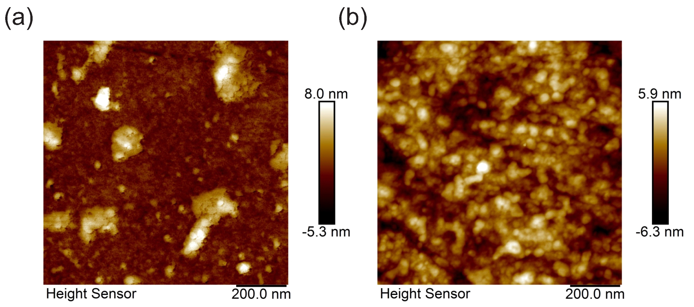
3.1. Atomic Force Microscopy Study of Cd 3 As 2 Films Grown by Non-Reactive Rf Magnetron Sputtering

Figure 1a,b shows typical 1 × 1 μ m 2 AFM images characterizing the surface morphology structure of the annealed Cd 3 As 2 films grown by non-reactive RF magnetron sputtering on the polished oriented single-crystalline (100)p-Si and (001) α -Al 2 O 3 wafers, respectively. The surface morphology of the Cd 3 As 2 /Si film sample (Figure 1a) exhibits prominent features represented by isolated 100–200 nm-sized equiaxed grains, which appear in bright contrast in the AFM image while scanning the film surface. The peculiar surface morphology was reported earlier for the magnetron-sputtered Cd 3 As 2 films, where it was also attested that this granular structure was not affected by annealing [5,6]. The recorded AFM image (Figure 1a) shows that the surface regions between large well isolated grains include smaller 10–30 nm-sized grains and even still smaller grains. These large and small protruding nanoisland structures seemingly characterize the initial stage of the Cd 3 As 2 film growth on the (100)p-Si substrates determined by the RF sputtering conditions promoting island growth. The island height is less than 10 nm, being about several times smaller than the film thickness, and the grown Cd 3 As 2 /Si films of about a 100 nm thickness are continuous. We would like to note that the scanning electron microscopy images of the Cd 3 As 2 films exhibiting the sub-Kelvin superconductivity without any external stimuli [6] revealed a similar surface morphology as the grainy surface structure of the Cd 3 As 2 /Si film shown in Figure 1a. By contrast, the surface morphology of the Cd 3 As 2 /Al 2 O 3 film sample is different as demonstrated by the AFM image shown by Figure 1b. One can see that here, the grainy morphology structure of the film is represented by relatively small grains having a size of about 10–30 nm, where the grains are closely situated to each other. Seemingly, these small nanoislands characterize the initial stage of the Cd 3 As 2 film growth on the (001) α -Al 2 O 3 substrates determined by the RF sputtering and [112] texturing conditions. The island height is less than 10 nm, so relatively thick Cd 3 As 2 /Al 2 O 3 films with thicknesses several times higher than the island height can be regarded as continuous.

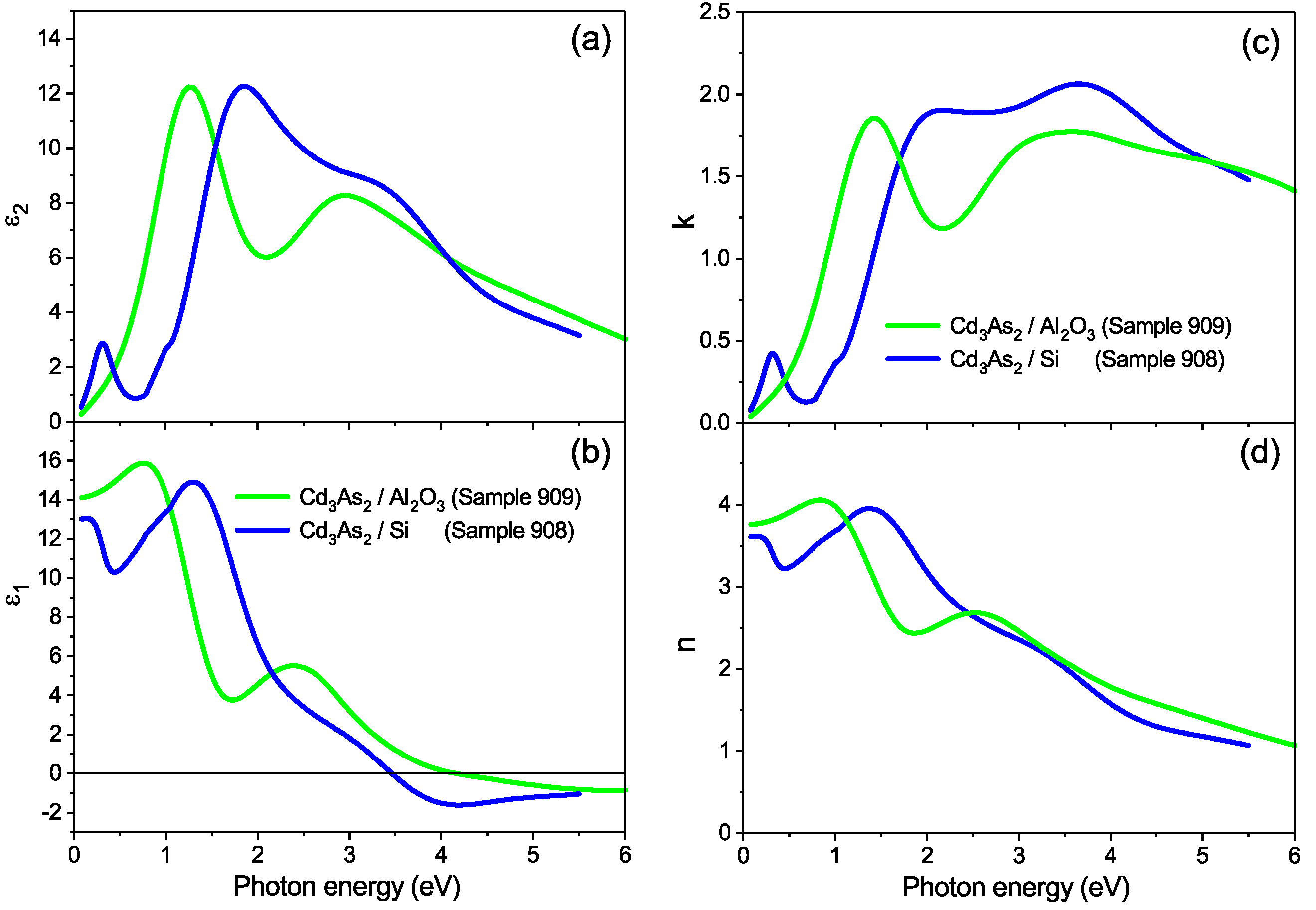
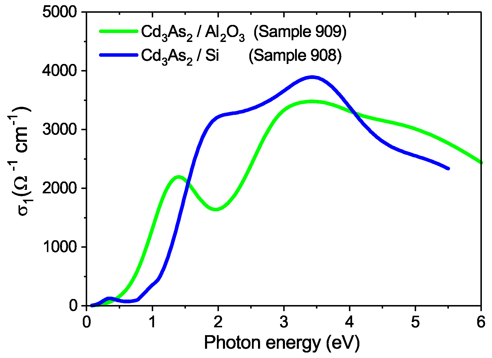
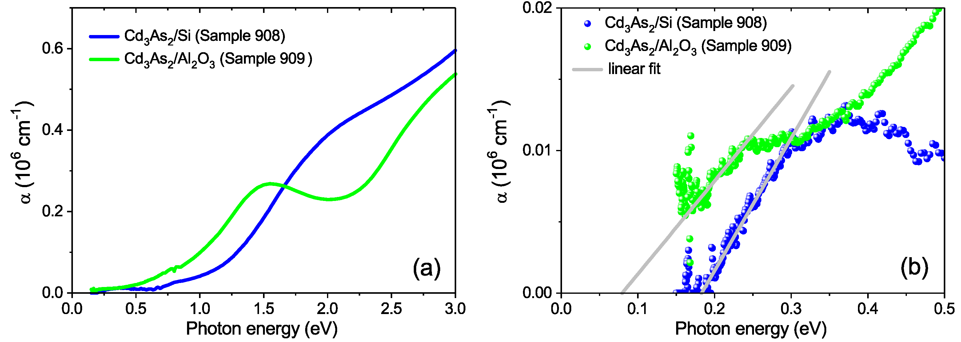
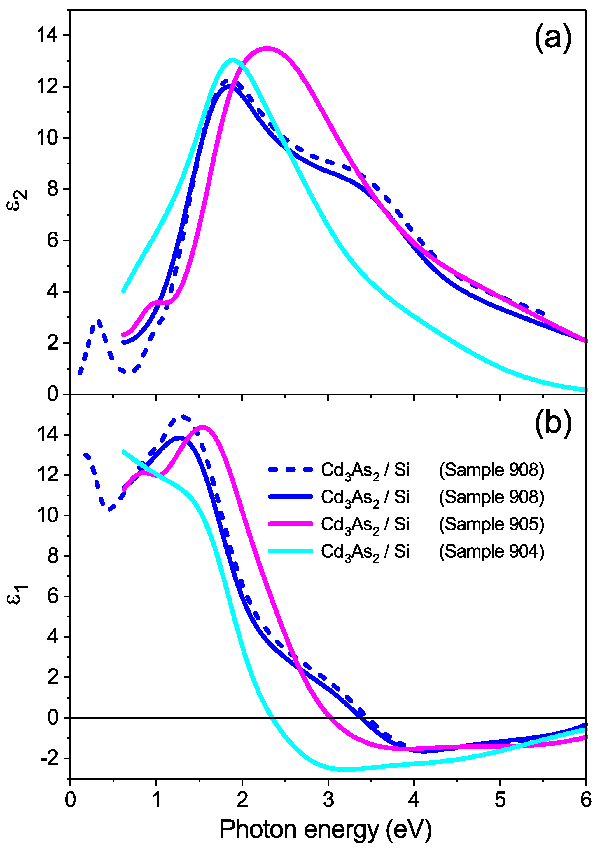
3.2. Spectroscopic Ellipsometry Study of the Cd 3 As 2 Films

The complex dielectric function spectra, ε ˜ ( ω ) = ε 1 ( ω ) + i ε 2 ( ω ) , of the investigated Cd 3 As 2 /Si and Cd 3 As 2 /Al 2 O 3 film samples were probed in the wide photon energy range of 0.02–8.5 eV with a set of three J.A. Woollam spectroscopic ellipsometers: IR-VASE Mark II, VASE, and VUV-Gen II. The ellipsometric angles Ψ ( ω ) and Δ ( ω ) were measured at two or three angles of incidence of 60 , 65 , and 70 at room temperature. The obtained ellipsometric angles Ψ ( ω ) and Δ ( ω ) were simulated in the framework of the bilayer model for the Cd 3 As 2 /Si and Cd 3 As 2 /Al 2 O 3 film samples using the J.A. Woollam VASE software [7] following the same approach as presented in more detail in our recent study of metallic Ta films [9].
The complex dielectric function ε ˜ ( ω ) = ε 1 ( ω ) + i ε 2 ( ω ) of a Cd 3 As 2 layer was modeled by the multiple Gaussian functions:
ε ˜ ( E ω ) = ε + n ε ˜ G a u s s n = ε + n ε 1 n + i ε 2 n ,
ε 2 n = A n e E E n σ 2 A n e E + E n σ 2 ,
σ = γ n 2 l n ( 2 ) ,
where ε is the high-frequency dielectric constant, which takes into account the contribution of the high-energy interband transitions. The adjustable Gaussian parameters were E n , γ n , and A n of the peak energy, the half width at half maximum, and the ε 2 peak height, respectively.
In the simulation of the ellipsometric angles, Ψ ( ω ) and Δ ( ω ) , the Cd 3 As 2 layers at the Si and Al 2 O 3 substrates were described by different multiple Gaussian dispersion models using Equation (1). For the multiple Gaussian model utilized, the complex dielectric function spectra of the blank Si and Al 2 O 3 substrates were substituted by the tabular complex dielectric function spectra [8]. The quality of the fit for the studied Cd 3 As 2 /Si and Cd 3 As 2 /Al 2 O 3 film samples was verified by the coincidence with the recorded ellipsometric angles Ψ ( ω ) and Δ ( ω ) within the specified accuracy lower than 5%. The good quality of the fit allowed us to estimate the actual film thickness of the films under study. From the multiple Gaussian model simulations by using Equation (1), the imaginary and real parts of the complex dielectric function spectra, ε 2 ( ω ) and ε 1 ( ω ) , as well as the imaginary and real parts of the complex refractive index, k and n, and the optical conductivity and absorption spectra of the Cd 3 As 2 layer on the Si and Al 2 O 3 substrates were obtained as displayed in Figure 2, Figure 3, Figure 4 and Figure 5.
From Figure 2a,b, one can monitor the properties of the complex dielectric function spectra for the annealed Cd 3 As 2 films grown by non-reactive RF magnetron sputtering on the polished oriented single-crystalline substrates (100)p-Si and (001) α -Al 2 O 3 . We found that, on the one hand, the dielectric response of the annealed Cd 3 As 2 /Al 2 O 3 film measured in the wide spectral range manifests two clearly pronounced interband optical transitions peaking at around 1.2 and 3.0 eV. On the other hand, the wide-range complex dielectric response measured for the annealed Cd 3 As 2 /Si film looks notably different. Namely, the evidently pronounced peak appears here at low photon energies at ∼0.36 eV. In addition, the main interband optical transitions are shifted to higher energies to 1.9 and 3.5 eV. Figure 3 shows the associated optical conductivity spectra, σ 1 ( ω ) = 1 4 π ω ε 2 ( ω ) , which follow the main trends observed in their complex dielectric function spectra. Figure 4a,b shows the optical absorption spectra for the annealed Cd 3 As 2 films in the wide range of the photon energies, where we also give a more detailed absorption at the low-energy edge. We discovered that the low-energy absorption edge of the investigated films exhibits linear dispersion, which is shifted to the higher energies and, therefore, more clearly pronounced for the annealed Cd 3 As 2 /Si film. We found that the low-energy absorption edge can be well described by the parameters of linear extrapolation (for more detail, see Figure 4b).
Here, we also investigated the as-grown Cd 3 As 2 films prepared by non-reactive RF magnetron sputtering on the Si substrates, which exhibited the peculiar morphology properties shown in Figure 1a. We would like to note that namely for the as-grown films, the sub-Kelvin SC is reported, which occurred without any external stimuli [6]. The optical properties of the as-grown films were probed by using a J.A. Woollam VASE spectroscopic ellipsometer in the spectral range from 0.5 to 6.0 eV, and the result of the model simulations is presented in Figure 5a,b. One can notice from the figure that the as-grown Cd 3 As 2 /Si samples show modified optical properties in the whole studied spectral range, as at the low energies, so in the range of the main interband transitions. Here, in comparison to the annealed Cd 3 As 2 /Si film, the low-energy feature may disappear or shift to the higher energy of 1 eV. At the same time, the first interband transition may show a noticeable blue shift to the higher energy of about 2.2 eV.

4. Discussion

The imaginary part of the dielectric function spectra (see Figure 2a) displaying two main electronic interband transitions at 1.2 and 3.0 eV for the annealed Cd 3 As 2 /Al 2 O 3 film is in perfect agreement with the theoretical calculations for the body centered tetragonal Cd 3 As 2 crystal by Conte et al. (see Figure 10 in [10]). From these theoretical calculations, no appreciable anisotropy is foreseen for the in-plane ( ε x x + ε y y ) / 2 and out-of-plane ε z z components. However, the wide range dielectric response measured for the annealed Cd 3 As 2 film/Si looks notably different. Namely, the evidently pronounced peak appears here at low photon energies at ∼0.36 eV. In addition, the main interband optical transitions are shifted to the higher energies of 1.9 and 3.5 eV. We attribute the observed difference in the dielectric function spectra to the effect of different doping associated with cadmium non-stoichiometry in the annealed Cd 3 As 2 /Al 2 O 3 and Cd 3 As 2 /Si films.
In Figure 4b, we present the optical absorption spectra, α ( E ω ) , obtained from the modeling of the SE data using a commercial WVASE32 software package [7]. We found that the low-energy absorption edge of the annealed Cd 3 As 2 /Si film is better described by the linear dependence at the lowest measured photon energies from 0.18 to 0.3 eV, compared to the commonly applied Tauc-type dependencies for direct, α E 2 E E d , and indirect, α E 1 / 2 E E i , gaps. The observed absorption characterized by the linear dispersion can be associated with the conical absorption. Indeed, due to conical dispersions, the optical absorption of 3D massless Kane particles is proportional to the frequency ω or to the photon energy ( E ω ) [11,12,13], distinctly in contrast with the frequency-independent optical conductivity of 2D Dirac electrons as observed in graphene [14,15,16]. Massless Kane electrons, which are not symmetry protected, may exist in a semiconductor with a nearly vanishing gap. We suggest that due to the doping effect, the conical Cd(s) conduction band minimum is shifted in energy above the heavy-flat As(p) valence band by about 0.183 ± 0.007 eV in the annealed Cd 3 As 2 /Si film, determining the optical gap value. Here, the maximum appearing at ∼ 0.36 eV can be associated with the absorption threshold developing near 0.3 eV. This can also reasonably explain the observed blue shift occurring for the main electronic transitions, which appear at 1.9 and 3.5 eV. By contrast, the linear dispersion due to conical absorption in the annealed Cd 3 As 2 /Al 2 O 3 seems to appear at the lower energy around 0.08 ± 0.01 eV, determining the value of the optical gap in accord with the linear extrapolation to zero photon energies. We note that because of the lack of reliable data at low photon energies, the given linear approximation may not be very accurate. Here, the low-energy feature becomes substantially weakened. This also results in smooth crossover from the conical to interband absorption. A variety of other investigated as-grown and annealed Cd 3 As 2 films/Si (see Figure 5) illustrates that pronounced changes of the electronic band structure take place at low energies due to the conical absorption, as well as in the range of interband transitions due to Cd non-stoichiometry (doping effect). The low- and high-energy trends seem to be in correlation, as discussed above.
Another issue is related to the possibility of the observation of SC related to 3D Dirac massless fermions, which was reported to exist below 300 mK for the as-grown Cd 3 As 2 films prepared by non-reactive RF magnetron sputtering (as those investigated in the present study) by Suslov et al. [6]. In Figure 5a,b, we show the complex dielectric function spectra of the as-grown Cd 3 As 2 /Si films along with the annealed Cd 3 As 2 film/Si. The dielectric function spectra for the as-grown samples look notably different at low energies, as well as in the range of interband transitions. As we have discussed, this can be explained by the shift in energy of the conical Cd(s) node, which is strongly dependent on the cadmium stoichiometry due to the doping effect. The SC properties necessarily disappear in the annealed films under study due to the opening of the gap, which can be beyond the field to find new SC properties associated with 3D Dirac fermions there. Then, one might suggest that a slight deviation from the intrinsic stoichiometry peculiar to Cd 3 As 2 single crystals leading to the appearance of the conical bands very close to the heavy-flat As(p) valence band around the Γ point in the Brillouin zone may be the necessary, but certainly not sufficient condition for the search for the new SC properties due to 3D Dirac massless fermions in Cd 3 As 2 films. Indeed, the symmetry-protected 3D Dirac particles, if existing in Cd 3 As 2 , may appear in a very short energy scale given by the crystal field splitting (at most a few tens of meV).

5. Conclusions

In summary, here, using atomic force microscopy and wide-range (0.02–8.5 eV) spectroscopic ellipsometry, we studied the morphology and optical properties of the as-grown and annealed Cd 3 As 2 /Si and Cd 3 As 2 /Al 2 O 3 films prepared by RF magnetron sputtering. The AFM study of the Cd3As2 films implies that the films are continuous and have a granular structure with island incorporation during the film growth. The complex dielectric function of the annealed Cd 3 As 2 /Al 2 O 3 film manifests pronounced interband optical transitions at 1.2 and 3.0 eV, in excellent agreement with the theoretical calculations for the body centered tetragonal Cd 3 As 2 crystal by Conte et al. [10]. The dielectric function response for the annealed Cd 3 As 2 /Si film looks notably different, where the evidently pronounced peak appears at low photon energies at ∼ 0.36 eV. We found that the absorption edge near the low-energy feature exhibits a linear dependence and can be associated with the conical absorption. The Cd(s) conical node is shifted in energy above the heavy-flat As(p) valence band by about 0.183 ± 0.007 eV, determining the optical gap value. The as-grown Cd 3 As 2 /Si films exhibit the pronounced changes of the electronic band structure due to Cd non-stoichiometry (doping effect), where the low-energy feature may disappear, signaling gapless electronic band structure. In principal, the conical dispersion at the point of the semiconductor to semimetal topological transition can be achieved by fine-tuning of cadmium concentration. However, since the symmetry-protected 3D Dirac particles may appear in a very short energy scale, insufficient sample quality (inhomogeneous chemical composition and high unintentional doping) might severely complicate this task.

Author Contributions

N.K., L.F., D.C., and A.M. contributed equally to the work reported. All authors read and agreed to the published version of the manuscript.

Funding

This research received no external funding.

Acknowledgments

We thank Kochura for providing us with the Cd 3 As 2 film samples. We thank Yu. A. Aleshchenko for useful discussions. The work of N.N.K. is carried out within the state assignment of the Ministry of Science and Higher Education of the Russian Federation (theme “Physics of condensed matter: new materials, molecular and solid state structures for nanophotonics, nanoelectronics, and spintronics”).

Conflicts of Interest

The authors declare no conflict of interest.

Abbreviations

The following abbreviations are used in this manuscript:
DSMDirac semimetals
AFMAtomic force microscopy
SESpectroscopic ellipsometry
SCSuperconductivity
XRDX-ray diffraction

References

  1. Wang, S.; Lin, B.-C.; Wang, A.-Q.; Yu, D.; Liao, Z.-M. Quantum transport in Dirac and Weyl semimetals: A review. Adv. Phys. X 2017, 2, 518–544. [Google Scholar]
  2. Armitage, N.P.; Mele, E.J.; Vishwanath, A. Weyl and Dirac semimetals in three-dimensional solids. Rev. Mod. Phys. 2018, 90, 015001. [Google Scholar] [CrossRef] [Green Version]
  3. Sato, M.; Ando, Y. Topological superconductors: A review. Rep. Prog. Phys. 2017, 80, 076501. [Google Scholar] [CrossRef] [PubMed] [Green Version]
  4. He, L.; Jia, Y.; Zhang, S.; Hong, X.; Jin, C.; Li, S. Pressure-induced superconductivity in the three-dimensional topological Dirac semimetal Cd3As2. NPJ Quantum Mater. 2016, 1, 16014. [Google Scholar] [CrossRef]
  5. Kochura, A.V.; Zakhvalinskii, V.S.; Htet, A.Z.; Ril’, A.I.; Pilyuk, E.A.; Kuz’menko, A.P.; Aronzon, B.A.; Marenkin, S.F. Growth of thin cadmium arsenide films by magnetron sputtering and their structure. Inorg. Mater. 2019, 55, 879–886. [Google Scholar] [CrossRef]
  6. Suslov, A.V.; Davydov, A.B.; Oveshnikov, L.N.; Morgun, L.A.; Kugel, K.I.; Zakhvalinskii, V.S.; Pilyuk, E.A.; Kochura, A.V.; Kuzmenko, A.P.; Pudalov, V.M.; et al. Observation of sub-kelvin superconductivity in Cd3As2 thin films. Phys. Rev. B 2019, 99, 094512. [Google Scholar] [CrossRef] [Green Version]
  7. Woollam, J.A. VASE Spectroscopic Ellipsometry Data Acquisition and Analysis Software; J.A. Woollam Co.: Lincoln, NE, USA, 2010. [Google Scholar]
  8. Palik, E.D. Handbook of Optical Constants of Solids; Elsevier Science: San Diego, CA, USA, 1991. [Google Scholar]
  9. Kovaleva, N.; Chvostova, D.; Dejneka, A. Localization phenomena in disordered tantalum films. Metals 2017, 7, 257. [Google Scholar] [CrossRef]
  10. Conte, A.M.; Pulci, O.; Bechstedt, F. Electronic and optical properties of topological semimetal Cd3As2. Sci. Rep. 2017, 7, 45500. [Google Scholar] [CrossRef] [PubMed] [Green Version]
  11. Akrap, A.; Hakl, M.; Tchoumakov, S.; Grasse, I.; Kuba, J.; Goerbig, M.O.; Homes, C.C.; Caha, O.; Novák, J.; Teppe, F.; et al. Magneto-optical signature of massless Kane electrons in Cd3As2. Phys. Rev. Lett. 2016, 117, 136401. [Google Scholar] [CrossRef] [PubMed] [Green Version]
  12. Orlita, M.; Basko, D.M.; Zholudev, M.S.; Teppe, F.; Knap, W.; Gavrilenko, V.I.; Mikhailov, N.N.; Dvoretskii, P.; Neugebauer, P.; Faugeras, C.; et al. Observation of three-dimensional massless Kane fermions in a zinc-blende crystal. Nat. Phys. 2014, 10, 233. [Google Scholar] [CrossRef] [Green Version]
  13. Timusk, T.; Carbotte, J.P.; Homes, C.C.; Basov, D.N.; Sharapov, S.G. Three-dimensional Dirac fermions in quasicrystals as seen via optical conductivity. Phys. Rev. B 2013, 87, 235121. [Google Scholar] [CrossRef] [Green Version]
  14. Kuzmenko, A.B.; van Heumen, E.; Carbone, F.; van der Marel, D. Universal optical conductance of graphite. Phys. Rev. Lett. 2008, 100, 117401. [Google Scholar] [CrossRef] [PubMed] [Green Version]
  15. Nair, R.R.; Blake, P.; Grigorenko, A.N.; Novoselov, K.S.; Booth, T.J.; Stauber, T.; Peres, N.M.R.; Geim, A.K. Fine structure constant defines visual transparency of graphene. Science 2008, 320, 1308. [Google Scholar] [CrossRef] [PubMed] [Green Version]
  16. Kovaleva, N.N.; Chvostova, D.; Potucek, Z.; Cho, H.D.; Fu, X.; Fekete, L.; Pokorny, J.; Bryknar, Z.; Kugel, K.I.; Dejneka, A.; et al. Efficient green emission from edge states in graphene perforated by nitrigen plasma treatment. 2D Mater. 2019, 6, 045021. [Google Scholar] [CrossRef] [Green Version]
Figure 1. Typical AFM images of the surface morphology of the Cd 3 As 2 films grown by non-reactive RF magnetron sputtering on the polished oriented single-crystalline wafers (a) (100)p-Si and (b) (001) α -Al 2 O 3 . The scan size is 1 × 1 μ m 2 .
Metals 10 01398 g001
Figure 2. (a,c) The imaginary parts of the dielectric function ε 2 ( ω ) and refractive index k and (b,d) the real parts of the dielectric function ε 1 ( ω ) and refractive index n for the annealed Cd 3 As 2 /Si (sample 908, 10 W, 80 min, 20 min annealing at 520 K) and Cd 3 As 2 /Al 2 O 3 (sample 909, 10 W, 40 min, 20 min annealing at 520 K) films, shown by solid blue and green curves, respectively. The thickness estimated from the model simulations was 91 ± 5 nm for the Cd 3 As 2 /Si film and 46 ± 3 nm for the Cd 3 As 2 /Al 2 O 3 film.
Metals 10 01398 g002
Figure 3. The respective optical conductivity spectra, σ 1 ( ω ) = 1 4 π ω ε 2 ( ω ) , for the annealed Cd 3 As 2 films.
Metals 10 01398 g003
Figure 4. The absorption spectra α ( ω ) for the annealed Cd 3 As 2 /Si and Cd 3 As 2 /Al 2 O 3 films shown for (a) the wide spectral range and (b) at the low-energy edge (shown by solid blue and green curves and symbols, respectively). The gray solid lines show linear extrapolations ( y = a + b x ) of the low-energy absorption edge (for Cd 3 As 2 /Si: a = 0.017 ± 2 % , b = 0.093 ± 2 % and for Cd 3 As 2 /Al 2 O 3 : a = 0.005 ± 9 % , b = 0.065 ± 4 % ).
Metals 10 01398 g004
Figure 5. (a,b) The imaginary ε 2 ( ω ) and real ε 1 ( ω ) parts of the complex dielectric function of the as-grown Cd 3 As 2 films on the polished oriented single-crystalline wafers (100)p-Si. The dashed blue curve corresponds to the data shown by the solid blue line in Figure 2. The solid blue, cyan, and magenta curves correspond to the ellipsometry measurements for Samples 908 (annealed), 904 (as-grown, 10 W, 20 min), and 905 (as-grown, 10 W, 80 min), respectively, obtained using a J.A. Woollam VASE ellipsometer.
Metals 10 01398 g005
Publisher’s Note: MDPI stays neutral with regard to jurisdictional claims in published maps and institutional affiliations.

