Abstract
In order to meet the defect-detection requirements of chips in high-precision surface mount technology (SMT) equipment widely used in the electronic industry, a chip appearance defect-detection method based on multi-order fractional discrete wavelet packet decomposition (DWPD) is proposed in this paper. First, lead and body regions were extracted from chip images using the image segmentation algorithm with asymmetric Laplace mixture model and connected-component labelling algorithm; then, the texture feature of the region to be inspected was extracted with the multi-order fractional DWPD algorithm and the geometric and gradient features were combined to form image features of the region to be inspected before the subset of features was selected from image features with the feature selection algorithm based on the variational Bayesian Gaussian mixture model; and finally, the support vector machine was used to determine whether the region to be inspected was defective. An experiment was conducted on a data set captured in high-precision SMT equipment. The accuracy of the proposed chip appearance defect-detection method is about 93%, which is more accurate than existing ones.
1. Introduction
High-precision surface mount technology (SMT) equipment plays an important role in the electronic manufacturing field. The high-precision placement machine, a typical high-precision SMT equipment, is used to mount the chip onto the print circuit board (PCB) accurately so that electronic equipment can realize the designed functions. Integrating software, algorithm, machine, control, optical, and other technologies, it is the most important and complex equipment in the manufacturing of electronic equipment [1,2]. Recently, more and more researchers are paying attention on the key technologies of high-precision placement machine [3,4].
With the rapid development of SMT placement machines, the size of components is becoming smaller and the assembly density of SMT patch is becoming higher. Among the various problems in placement machines, inspecting appearance defects on the electronic chip before the chip is mounted onto the PCB are receiving increasing attention. As shown in Figure 1, common appearance defects of chips in electronic manufacturing include contaminated areas on lead surfaces, burrs on lead edges, and scratches on chip bodies. The contaminated area on a lead surface refers to the oil or rusty stain on the lead. Lead with such defects cannot be fixed to the PCB bonding pad by soldering, leading to poor contact of the chip or the chip peeling off from the PCB. A burr on the lead edge will concentrate soldering around the burr, short-circuiting the PCB. A scratch on the chip body shows that the chip has frictions with other objects and that the resultant static electricity may have damaged the internal circuit of the chip. Any electronic chip with such a defect used in production will cause serious failure of the electronic equipment or even serious potential risks. Therefore, a chip appearance defect-detection method is one of the key technologies urgently needed in the development of placement machines.
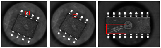
Figure 1.
Appearance defects on an electronic chip.
Researchers have conducted a lot of work on electronic chip appearance defect detection. A lead defect-detection algorithm based on template matching and colour contrast was proposed in [5]. With this algorithm, lead positions and colour defects can be inspected, but it is impossible to determine whether there is any contaminated area on the lead surface of a chip and whether there is any scratch on the chip body. Furthermore, a defect-detection method based on image feature and support vector machine was presented in [6,7]. The image features include geometric, grey, and texture features. However, the texture feature cannot reflect the change in image texture using multiple scales. A work by [8] investigated an electronic chip inspection system based on stereoscopic vision, by which the stereoscopic information of an electronic chip can be obtained with a complex three-axis control platform. The work in [9] developed several methods to inspect defects in the flip chip solder joints. In [10], some problems when inspecting defects in industrial applications were reviewed, and the texture based method is shown to be widely used to solve those problems. Also, the work in [11] investigated a segment-based method to detect grain surface defects in the chip industry. The algorithms proposed by the researches mentioned above meet the requirements of the industrial electronic manufacturing field for surface defect detection to some extent. Among these algorithms, the chip appearance defect detection based on a wavelet is more popular with higher accuracy [12,13], which remains unsolved.
On the other hand, wavelet transform technology and wavelet packet decomposition (WPD) technology are widely utilized in texture feature extraction. The work in [14] processed texture images with wavelet transform and applied mean and standard deviation as wavelet statistical characteristics. Furthermore, WPD was adopted in [15] instead ofwWavelet transform in texture feature extraction, and the daubechies filter, symlets filter, and biorthogonal filter were compared in wavelet transform in [16]. The work in [17] spread 2D wavelet transform into 3D wavelet transform to extract spectral characteristics from hyper-spectral remote sensing images. Furthermore, the singular value decomposition (SVD) algorithm was used to enhance images before wavelet transforming in [18]. However, the chip appearance defect detection based on multi-order fractional WPD remains unsolved.
Contributions of this paper. The contributions of our work are listed as follows:
- A multi-order fractional DWPD algorithm is proposed to extract features from chip images.
- The clustering algorithm based on the variational Bayesian Gaussian mixture model is adopted to select image features.
- A chip appearance defect-detection method based on the multi-order fractional DWPD is conducted.
Organization of this paper. The rest of this paper is organised as follows. The background on DWPD and multi-order fractional DWPD are presented in Section 2. The main results on chip appearance defect detection based on multi-order fractional DWPD are proposed in Section 3. Section 4 presents the experiment on a high-precision SMT equipment to estimate the effectiveness of the proposed method, and Section 5 concludes this paper.
2. Background
2.1. Discrete Wavelet Packet Decomposition
The 1D discrete wavelet transform (DWT) can be realized with a multi-layer transform structure. High-pass filters and low-pass filters are used to process the input signal in each layer of transform, with the high-pass filter outputting a precise detailed part of the input signal and with the low-pass filter outputting the rough approximation part. According to the Nyquist sampling theorem, the highest frequency of the filtered signal is only half of its original signal. Therefore, it is necessary to halve the data length by downsampling after the signal is processed by two groups of filters. In the 1D DWT, the input signal is taken as the input at the first layer and the rough approximation part of the previous layer is taken as the input at each subsequent layer. A layer of DWT is expressed as [19]:
where x is the input signal, is the precise detail part, is the rough approximation part, h is the high-pass filter coefficient, and l is the low-pass filter coefficient. h and l are a group of quadrature mirror filters meeting the following condition:
where N is the length of the filter coefficient.
The 2D DWT can be realized with a similar multi-layer transform structure. The layer of wavelet transform defined by Equation (1) is conducted in the row and column directions successively in each layer of transform. Equation (1) discomposes the input signal into two parts. Therefore, the input signal is decomposed into four parts by the single layer transform in 2D DWT, including the output processed by the low-pass filter in the row and column directions successively as the rough approximation part as well as all other three outputs as the precise detail part. Similar to 1D DWT, the input signal is taken as the input at the first layer, and the rough approximation part of the previous layer is taken as the input at each subsequent layer.
What should be mentioned is that only the rough approximation part of the previous layer in the above 1D DWT and 2D DWT is processed at each layer, while all other precise detail parts are ignored. Therefore, too much detailed information is lost in the transform process. To address this problem, the discrete wavelet packet decomposition (DWPD) algorithm is adopted to extract features. What should be mentioned is that the multi-layer transform structure in 1D DWPD and 2D DWPD is similar to that in DWT and the filters in 1D DWPD and 2D DWPD are the same as that in DWT at each layer. In the multi-layer transform structure, the input signal is taken as the input at the first layer, while each output of the previous layer is taken as the input at each subsequent layer.
2.2. Multi-Order Fractional Discrete Wavelet Packet Decomposition
Before presenting the main results on chip appearance defect detection, the basic definitions on multi-order fractional DWPD are given in this section. By adding an extra transform-order parameter to the Fourier transform, fractional Fourier transform is defined as follows [20,21]:
where p is the order of fractional Fourier transform and is the kernel function of fractional Fourier transform, which is defined as follows:
where n is an integral and is the Dirac function that meets the following conditions:
and where is defined as follows:
The period of the order p of the fractional Fourier transform defined by Equation (4) is 2, usually restricting the order within . Furthermore, it is not difficult to find that the fractional Fourier transform has the property of , further restricting the order within .
Based on the discrete sampling method proposed in [22], 1D discrete fractional Fourier transform is defined as follows:
where I is the N long input discrete signal and is the matrix of . The element with a label of is defined as follows:
and and are the diagonal matrix of . Elements with the label are defined as follows:
where and are the sampling intervals of the time domain and fractional Fourier transform domain, respectively, and meet the following condition:
Similar to the 2D discrete Fourier transform, the 1D discrete fractional Fourier transform defined by Equation (7) is conducted in the row and column directions successively to obtain the results of 2D discrete fractional Fourier transform. In this paper, if the orders in both directions are p, then the 1D discrete fractional Fourier transform is called a p-order 2D discrete fractional Fourier transform.
What should be mentioned is that the 2D fractional DWPD algorithm [23] can be obtained by combining 2D discrete fractional Fourier transform and 2D DWPD. In 2D fractional DWPD, the input signal is processed by the p-order 2D discrete fractional Fourier transform first, and then, the results of the previous steps are processed by the 2D DWPD to obtain the results of p-order 2D fractional DWPD. According to the properties of discrete fractional Fourier transform, the order of 2D fractional DWPD is within .
3. Chip Appearance Defect Detection Based on Multi-Order Fractional DWPD
3.1. Steps of the Appearance Defect-Detection Method
As shown in Figure 2, the appearance defect-detection method researched in this paper is carried out according to following steps:
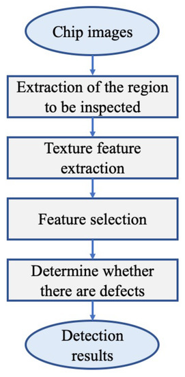
Figure 2.
Flowchart of the proposed method.
- (1)
- Extract the lead and body regions from chip images using the image segmentation algorithm with the asymmetric Laplace mixture model [24] and connected-component labelling algorithm;
- (2)
- Extract the image features of the region to be inspected, including the multi-order fractional DWPD-based texture feature, the Hu moment invariant [25]-based geometric feature, and the blueHistogram of Oriented Gradient (HoG) [26]-based gradient feature;
- (3)
- Select the image features of the region to be inspected;
- (4)
- Determine whether the region to be inspected is defective with the support vector machine-based classifier and extracted image features.
3.2. Extraction Algorithm of the Region to Be Inspected
In this section, the region to be inspected is extracted using the image segmentation algorithm with the asymmetric Laplace mixture model and connected-component labelling algorithm. As shown in Figure 1, a chip image includes three regions: the lead region, the body region, and the background region. The body and lead of an electronic chip consist of opaque plastic and bright-colored sheet metal, respectively, and are displayed as a black region and a white region on the chip image, respectively. The background of the chip image is displayed as black in the placement machine but with possible small white jamming regions. That is, when a complete chip image is processed by the chip defect-detection method directly, the inspection method may mistake jamming regions in the background of the chip image as chip defects, which will affect the accuracy of the detection method. To handle this problem, the lead and body regions are extracted from the chip image as the regions to be processed in subsequent steps before inspecting chip defects.
In the high-precision placement machine, the chip is often not in the center of the image and has a certain rotation angle; therefore, it is necessary to locate the position of the chip image. In addition, there may be jamming regions in the background of the chip image under the influence of ambient light and background region, which will lower the accuracy of the chip positioning. Therefore, the algorithm extracting the region to be inspected from the chip image is carried out according to the following steps:
- (1)
- Classify pixels of the chip image into two categories using the image segmentation algorithm with the asymmetric Laplace mixture model, among which the one with a larger average grey value is the potential lead pixel of the chip image.
- (2)
- Calculate the connected components of potential lead pixels in the chip image using the connected-component labelling algorithm, and take these regions as the potential lead regions.
- (3)
- Estimate the bounding rectangles with rotation angles for each potential lead region, and calculate their rectangularity using the following equation:where is the area of the potential lead region, i.e., pixels, and is the area of the bounding rectangle with a rotation angle.
- (4)
- Identify the regions for which the size does not meet the standard or for which the rectangle is too small in the potential lead regions as jamming regions, and then, eliminate these regions from the potential lead regions. If the number of screened lead regions is inconsistent with that of the standard chip, the chip is considered to have the defect “the number of lead regions does not match”, and the subsequent defect-detection steps are stopped.
- (5)
- Estimate the bounding rectangle with a rotation angle of all lead pixels by taking the pixels in the screened lead region as the lead pixels of the chip, and take the position and rotation angle of the bounding rectangle as those of the chip in the image.
- (6)
- Rotate the chip image according to the rotation angle of the chip to make the chip horizontal in the image. The lead and body regions of the chip from the rotated image are extracted according to the parameters and position of the chip.
Then, the first step of the proposed chip appearance defect-detection method is accomplished.
3.3. Texture Feature Extraction Based on Multi-Order Fractional DWPD
The second step of the proposed chip appearance defect-detection method presented above is the texture feature extraction of the region to be inspected. The time-frequency domain analysis method based on WPD is a common texture feature extraction method. In the appearance defect detection for high-precision SMT, the appearance texture of the chip is quite complex, requiring expansion of the traditional transform-based feature extraction method to meet the requirements of an actual application.
The fractional DWPD algorithm introduced in Section 2.2 was applied in some image processing applications, including image encryption [23], image watermark increasing [27], etc. In these applications, the traditional DWPD was replaced by the fractional DWPD and the order was selected by the order estimation link. The fractional DWPD method performed well in the applications mentioned above. For example, in the application of image encryption, the unknown order of fractional DWPD was used to increase the difficulty of image decryption. However, image textures cannot be increased by this method.
For the problem mentioned above, a multi-order fractional DWPD structure was conducted in this paper to extract image features as shown in Figure 3. As shown in Figure 3, two methods were used for decomposition:
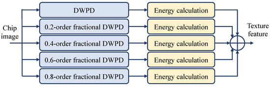
Figure 3.
The structure of multi-order factional discrete wavelet packet decomposition (DWPD).
- (1)
- The first case: The chip image was decomposed using the traditional 2D DWPD algorithm.
- (2)
- The second case: The chip image was decomposed with the 2D multi-order fractional DWPD algorithm. Since the value range of the order of 2D multi-order fractional DWPD algorithm was within , the chip image was decomposed by the 2D fractional DWPD algorithm of 0.2-order, 0.4-order, 0.6-order, and 0.8-order.
After the chip image was processed by the above multi-order fractional DWPD structure, the sub-frequency bands of the chip image were obtained and the energy of all the sub-frequency bands was combined as the texture features of the chip image. Then, the average value and standard deviation of the sub-frequency band were taken as the energy of the sub-frequency band in the texture feature extraction algorithm proposed in this paper. The average value and standard deviation of the sub-frequency band are given as following:
where C is the matrix of the sub-frequency band, and M and N are the length and width of C, respectively.
3.4. Image Feature Selection Based on Variational Bayesian Algorithm
The third step of the proposed chip appearance defect-detection method presented above is image feature selection. As mentioned above, in order to excavate the features of defects deeply, texture features, geometric features, and gradient features are combined in the process of image feature extraction. Some of these features may be correlated, which is ineffective for appearance defect detection or even causes “dimensional disaster” [28]. Therefore, it is necessary to select a subset of features from image features using the feature selection algorithm before classification with the support vector machine [29,30,31,32].
As is known, the clustering-based algorithm is a common image feature selection algorithm [33,34] and consists of two steps:
- (1)
- Cluster features with clustering algorithms such as k-means and minimum spanning tree so that the features of different classes are mutually independent.
- (2)
- Take the feature closest to the center of the class as the representative feature in each class, and compose the final feature subset of all the representative features of the class.
What should be mentioned is that features in the subset obtained through the above algorithm are independent of each other, providing better results for subsequent support vector machine algorithms.
In traditional clustering-based feature selection algorithms, it is required to provide the number of subsets of features. If the number of subsets of features given is wrong in the feature selection algorithm, the representative features are ignored, which affects the effect of chip detection. To solve this problem, the method proposed in this paper adopts a clustering algorithm based on the variational Bayesian Gaussian mixture model [21]. In the process of clustering, the algorithm determines the optimal number of subsets of features automatically instead of trying to obtain the optimal number of subsets of features by cross verification.
To present the process of a chip appearance defect-detection method based on multi-order fractional DWPD better, bluethe pseudocode are given in Algorithm 1.
| Algorithm 1 Pseudcode of the proposed method. |
| Input: Chip image I |
| Output: Whether the chip is defective |
|
4. Experimental Verification
4.1. Experimental Design
In order to verify the accuracy of the chip appearance defect-detection method proposed in this paper, an experiment is conducted on a high-precision SMT equipment.
As shown in Figure 4, the chip inspection module of the high-precision SMT equipment consists of a camera, lens, and light source. The camera is equipped with a 1/3-inch black and white charge coupled device (CCD) with a resolution of 1028 × 1024. The prime lens with a resolution of 1 million pixels is used for the lens. The light source consists of three ring light sources of 0°, 45°, and 60°. The chip detection module controls these three ring light sources (each having 16 brightness levels) by the Pulse Width Modulation (PWM) module. Different details of the chip can be reflected in the image by adjusting the brightness level of ring light source: The ring light source of 0° mainly reflects the flat part of the chip, that of 45° mainly reflects the edge of the chip, and that of 60° mainly reflects the uneven area of the chip.
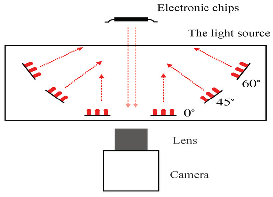
Figure 4.
Structure of the chip detection module
During the experiment, 30 chips with relevant appearance defects and 20 chips without defects in the electronic equipment production were collected. Chip images were collected under 12 light configurations with the high-precision SMT equipment, and the configurations of three ring light sources are shown in Table 1. As presented in Section 3, the lead and body regions are extracted from these chip images with image segmentation and connected-component labelling algorithms. Then, the regions obtained are manually labelled, and the lead region was marked as three categories: no defect, pollutant on the surface of the chip, and burr on the edge of the chip. The body region was marked as two categories: no defect and scratch on the body. Finally, the lead data set and the body data set were formed according to the results of manual labelling. What should be mentioned is that there are three types of data in the lead data set, each consisting of 200 samples, and there are two types of data in the body data set, each consisting of 200 samples. These types are splited into the training sets and test sets, which contain 120 samples and 80 samples, respectively. These training sets and test sets are gathered to generate training sets and test sets for the lead data set and body data set.

Table 1.
Twelve lighting configurations for image capture.
To evaluate the effectiveness of the proposed method, contrast experiments with the DWPD-based method and the cooccurence matrix based method were conducted with the same lead data set and body data set mentioned above. In the experiment, lead defect detectors and body defect detectors were trained with the lead train data set and body train data set and the detection results were estimated with the lead test set and body test set. In the test period, classification accuracy was calculated as follows:
4.2. Results and Discussion
The experiment results of these three methods are demonstrated in Table 2 and Table 3. As shown in Table 2 and Table 3, the performance of the proposed method outperforms the DWPD-based method and the cooccurrence matrix-based method. Furthermore, the accuracy of the proposed defect-detection method for lead without defects and pollutants on the lead surface and a body without defects and scratches on the body is more than 91%; specifically, the detection rate of a body without defects is more than 93%. However, the recognition rate is low for the defect with a burr on the edge of the pin. The main reason for these phenomena is that a chip with a larger burr size will be eliminated in the step extracting the region to be detected in the detection method, and this chip will be identified as the defect “the number of pin areas does not conform”. That is, only chips with small burr sizes will be tested for appearance defects, and the texture of these samples but will not differ much from those without defects. However, the small size of these burrs will not cause problems of electronic chip offset and pin short circuit, so there is almost no impact on product quality.
Table 2.
Classification accuracy for lead defect detection.
Table 3.
Classification accuracy for body defect detection.
A small data set consisting of 200 samples, which contains 120 samples for the training set and 80 samples for the test set, was used. In many cases, large data sets are not available in practical industrial electronic applications in which the relatively low accuracy is feasible and tolerated. If the number of samples for test data set is larger, the accuracy of the proposed method is higher and the cost of testing increases. The accuracy of chip defect detection may be up to 99% if the test set is large enough. That is, the accuracy of the proposed method is about 93%, which is higher than existing results with the same data set.
Furthermore, the proposed chip defect-detection method based on multi-order fractional DWPD cannot be applied to appearance defect-detection problems based on big data, which will be future work.
5. Conclusions
The requirement for high stability of the electronic equipment puts forward a high standard for chip defect detection in a high-precision placement machine. To solve this problem, a chip defect-detection method based on multi-order fractional DWPD was proposed in this paper. First, the image segmentation algorithm and connected-component labelling algorithm were utilized to extract the lead and body regions of the chip. Then, the complete region features were constructed by texture features based on the multi-order fractional DWPD algorithm, the geometric features were constructed based on the Hu invariant moment algorithm, and the gradient features were constructed based on the HoG algorithm. Finally, features were classified with the support vector machine to inspect the appearance defects of the chip. The proposed method was verified by experiments with pictures taken by actual equipment. The accuracy of the proposed method is about 93%, which is higher than existing results with the same data set. Furthermore, chip appearance defect detection based on a deep learning method will be considered in future work.
Author Contributions
Conceptualization, H.Z. and H.S.; data curation, H.S.; formal analysis, H.S.; funding acquisition, H.Z.; methodology, H.S.; project administration, H.S.; resources, H.S.; software, H.S.; supervision, P.S.; validation, P.S.; visualization, P.S.; writing—original draft, H.Z.; writing—review and editing, H.Z. All authors have read and agreed to the published version of the manuscript.
Funding
This work was supported by the National Natural Science Foundation of China (62003062), by the Science and Technology Research Project of Chongqing Municipal Education Commission (KJZD-M201900801 and KJQN201900831), by the Chonqqing Natural Science Foundation (cstc2020jcyj-msxmX0077), by the High-level Talents Research Project of CTBU (1953013, 1956030, and ZDPTTD201918), and by the Key Platform Open Project of CTBU (KFJJ2019062 and KFJJ2017075).
Institutional Review Board Statement
This article does not contain any studies with human participants or animals performed by any of the authors. All the experiments were conducted on computers via programming design.
Informed Consent Statement
Not applicable.
Data Availability Statement
The source codes and datasets used to support the findings of this study are available from the corresponding author upon request via email: sunhaohit0@gmail.com.
Conflicts of Interest
The authors declare no conflict of interest.
Abbreviations
The following abbreviations are used in this manuscript:
| SMT | Surface Mount Technology |
| WPD | Wavelet Packet Decomposition |
| DWT | Discrete Wavelet Transform |
| DWPD | Discrete Wavelet Packet Decomposition |
| CCD | Charge Coupled Device |
References
- Zhao, L.; Shi, P. Machine learning assisted aggregation schemes for optical cross-connect in hybrid electrical/optical data center networks. OSA Contin. 2020, 3, 2573–2590. [Google Scholar] [CrossRef]
- Gaggero, M.; Caviglione, L. Model predictive control for energy-efficient, quality-aware, and secure virtual machine placement. IEEE Trans. Autom. Sci. Eng. 2019, 16, 420–432. [Google Scholar] [CrossRef]
- Wang, H.; Zhou, A.; Hsu, C.-H.; Xiao, X.; Yang, F. Provision of data-intensive services through energy- and QoS-aware virtual machine placement in national cloud data centers. IEEE Trans. Emerg. Top. Comput. 2016, 4, 290–300. [Google Scholar] [CrossRef]
- Guo, Y.; Stolyar, A.L.; Walid, A. Shadow-routing based dynamic algorithms for virtual machine placement in a network cloud. IEEE Trans. Emerg. Top. Comput. 2018, 6, 209–220. [Google Scholar] [CrossRef]
- Xu, G. Appearance Inspection System of IC Chips Based on Machine Vision. Master’s Thesis, South China University of Technology, Guangzhou, China, 2010. [Google Scholar]
- Chao, Y. Research on Key Techniques for Semi-Conductor Chip Surface Defect Online Detection Based on Machine Vision. Ph.D. Thesis, Southeast University, Nanjing, China, 2017. [Google Scholar]
- Chen, K. Research on Key Technology for Integrated Circuit Chip Surface Defects Vision Detection. Ph.D. Thesis, Southeast University, Nanjing, China, 2016. [Google Scholar]
- Chen, J. Research and Development on the Stereo Vision Measurement System Based on IC Chip. Master’s Thesis, South China University of Technology, Guangzhou, China, 2012. [Google Scholar]
- Su, L.; Yu, X.; Li, K.; Pecht, M. Defect inspection of flip chip solder joints based on non-destructive methods: A review. Microelectron. Reliab. 2020, 110, 113657. [Google Scholar] [CrossRef]
- Czimmermann, T.; Ciuti, G.; Milazzo, M.; Chiurazzi, M.; Roccella, S.; Oddo, C.M.; Dario, P. Visual-based defect detection and classification approaches for industrial applications—A survey. Sensors 2020, 20, 1459. [Google Scholar] [CrossRef]
- Chen, X.; Zhao, C.; Chen, J.; Zhang, D.; Zhu, K.; Su, Y. K-means clustering with morphological filtering for silicon wafer grain defect detection. In Proceedings of the 2020 IEEE 4th Information Technology, Networking, Electronic and Automation Control Conference (ITNEC), Chongqing, China, 12–14 June 2020; pp. 1251–1255. [Google Scholar]
- Stefenon, S.F.; Ribeiro, M.H.D.M.; Nied, A.; Marianide, V.C.; Coelhobd, L.D.S.; da Rochaa, D.F.M.; Grebogifg, R.B.; Ruano, A.E.D. Wavelet group method of data handling for fault prediction in electrical power insulators. Int. J. Electr. Power Energy Syst. 2020, 123, 106269. [Google Scholar] [CrossRef]
- Frizzo Stefenon, S.; Zanetti Freire, R.; dos Santos Coelho, L.; Meyer, L.H.; Bartnik Grebogi, R.; Gouvêa Buratto, W.; Nied, A. Electrical insulator fault forecasting based on a wavelet neuro-fuzzy system. Energies 2020, 13, 484. [Google Scholar] [CrossRef]
- Arivazhagan, S.; Ganesan, L. Texture classification using wavelet transform. Pattern Recognit. Lett. 2003, 24, 1513–1521. [Google Scholar] [CrossRef]
- Huang, K.; Aviyente, S. Wavelet feature selection for image classification. IEEE Trans. Image Process. 2008, 17, 1709–1720. [Google Scholar] [CrossRef] [PubMed]
- Dua, S.; Acharya, U.R.; Chowriappa, P.; Sree, S.V. Wavelet-based energy features for glaucomatous image classification. IEEE Trans. Inf. Technol. Biomed. 2011, 16, 80–87. [Google Scholar] [CrossRef]
- Qian, Y.; Ye, M.; Zhou, J. Hyperspectral image classification based on structured sparse logistic regression and three-dimensional wavelet texture features. IEEE Trans. Geosci. Remote. Sens. 2012, 51, 2276–2291. [Google Scholar] [CrossRef]
- Chang, B.-M.; Tsai, H.-H.; Yen, C.-Y. SVM-PSO based rotation-invariant image texture classification in SVD and DWT domains. Eng. Appl. Artif. Intell. 2016, 52, 96–107. [Google Scholar] [CrossRef]
- Daubechies, I. Ten Lectures on Wavelets; Society for Industrial and Applied Mathematics: Philadelphia, PA, USA, 1992. [Google Scholar]
- Wang, X.; Xu, B.; Shi, P.; Li, S. Efficient learning control of uncertain fractional-order chaotic systems with disturbance. IEEE Trans. Neural Netw. Learn. Syst. 2020. [Google Scholar] [CrossRef]
- Tao, R.; Meng, X.; Wang, Y. Image encryption with multi-orders of fractional Fourier transforms. IEEE Trans. Inf. Forensics Secur. 2010, 5, 734–738. [Google Scholar] [CrossRef]
- Pei, S.-C.; Ding, J.-J. Closed-form discrete fractional and affine Fourier transforms. IEEE Trans. Signal Process. 2000, 48, 1338–1353. [Google Scholar]
- Bhatnagar, G.; Wu, Q.M.; Raman, B. Discrete fractional wavelet transform and its application to multiple encryption. Inf. Sci. 2013, 223, 297–316. [Google Scholar] [CrossRef]
- Sun, H.; Yang, X.Q.; Gao, H.J. A spatially constrained shifted asymmetric Laplace mixture model for the grayscale image segmentation. Neurocomputing 2019, 331, 50–57. [Google Scholar] [CrossRef]
- Hu, M.K. Visual pattern recognition by moment invariants. IRE Trans. Inf. Theory 1962, 8, 179–187. [Google Scholar]
- Dalal, N.; Triggs, B. Histograms of oriented gradients for human detection. In Proceedings of the IEEE Conference on Computer Vision and Pattern Recognition, San Diego, CA, USA, 20–26 June 2005. [Google Scholar]
- Bhatnagar, G.; Raman, B.; Wu, Q.J. Robust watermarking using fractional wavelet packet transform. IET Image Process. 2012, 6, 386–397. [Google Scholar] [CrossRef]
- Bishop, C.M. Pattern Recognition and Machine Learning; Information Science and Statistics; Springer: Cambridge, UK, 2007; 738p. [Google Scholar]
- Mahabub, A.; Mahmud, M.I.; Hossain, M.F. A robust system for message filtering using an ensemble machine learning supervised approach. ICIC Express Lett. Part B Appl. 2019, 10, 805–811. [Google Scholar]
- Murata, M.; Orikane, K.; Akae, R. Automatic selection and analysis of verb and adjective synonyms from Japanese sentences using machine learning. Int. J. Innov. Comput. Inf. Control 2019, 15, 2135–2147. [Google Scholar]
- Ahmad, T.; Aziz, M.N. Data preprocessing and feature selection for machine learning intrusion detection systems. ICIC Express Lett. 2019, 13, 93–101. [Google Scholar]
- Lin, H.-D.; Chen, H.-L. Detection of surface flaws on textured LED lenses using wavelet packet transform based partial least squares techniques. Int. J. Innov. Comput. Inf. Control 2019, 15, 905–921. [Google Scholar]
- Wang, L.X.; Jiang, S.Y. Novel feature selection method based on feature clustering. Appl. Res. Comput. 2015, 32, 1305–1308. [Google Scholar]
- Song, Q.B.; Ni, J.J.; Wang, G.T. A fast clustering-based feature subset selection algorithm for high-dimensional data. IEEE Trans. Knowl. Data Eng. 2013, 25, 1–14. [Google Scholar] [CrossRef]


Publisher’s Note: MDPI stays neutral with regard to jurisdictional claims in published maps and institutional affiliations. |
© 2021 by the authors. Licensee MDPI, Basel, Switzerland. This article is an open access article distributed under the terms and conditions of the Creative Commons Attribution (CC BY) license (http://creativecommons.org/licenses/by/4.0/).