1. Introduction
As the core carrier of modern electronic systems, the manufacturing quality of PCBs directly determines the performance stability and reliability of electronic devices and plays a pivotal role in the electronic information industry [
1,
2]. With the rapid development of electronic components towards high-density integration and miniaturization, PCB surface defect detection tasks face technical challenges such as increasingly refined defect features and more intricate backgrounds. During the manufacturing process, due to the influence of multiple factors including process complexity, equipment status, and environmental conditions, PCBs are prone to various surface defects such as open circuits, short circuits, and mouse bites [
3]. These defects not only lead to a decline in product yield but may also pose potential risks such as circuit function failure.
Currently, traditional PCB surface defect detection technologies mainly face two types of bottlenecks: First, manual visual inspection is easily constrained by factors such as operator experience and visual fatigue, with low recognition rates for micron-scale defects (such as micro-cracks and cold solder joints); Second, traditional algorithms based on Automatic Visual Inspection (AVI) and Automated Optical Inspection (AOI), although realizing automation of detection processes, rely heavily on manually designed feature engineering and rule libraries. In scenarios with complex defect morphologies (e.g., multi-scale defects and fuzzy-boundary defects), non-uniform illumination at industrial sites, and electromagnetic noise interference, the model’s generalization ability and robustness are insufficient [
4]. Existing methods have significant limitations in balancing detection accuracy, efficiency, and environmental adaptability, making it difficult to meet the urgent needs of intelligent manufacturing for high-precision and real-time detection.
In recent years, deep learning technology has provided innovative solutions for PCB defect detection through end-to-end feature learning mechanisms. In the current deep learning object detection algorithm system, two-stage algorithms are represented by Mask R-CNN [
5] and Faster-RCNN [
6], while one-stage algorithms are represented by SSD [
7] (Single Shot MultiBox Detector) and YOLO [
8,
9,
10] (You Only Look Once) series as typical examples. These two method types adopt different technical paths in balancing precision and speed.
To address the issue of noise robustness in PCB defect detection, Chen Renxiang et al. [
11] proposed an improved Faster R-CNN model by introducing a Split-attention Network module and an integrated balanced feature pyramid architecture and constructed an efficient collaborative fusion mechanism for multi-resolution features. Liu et al. [
12] enhanced PCB images through operations such as image smoothing, contrast enhancement, and sharpening, and accomplished defect recognition using a combination of digital morphology and threshold segmentation. Luo Renze et al. [
13] introduced a feature pyramid structure into the Faster R-CNN object detection framework and designed a three-branch region proposal network to optimize detection efficiency, effectively enhancing the model’s feature representation capability and enabling the coordinated improvement of precision and speed. Although the detection accuracy of two-stage algorithms continues to improve, their two-stage cascade structure leads to lower detection speeds and inferior small target detection performance, which significantly limits their use in certain practical application scenarios, particularly for real-time industrial detection.
Compared to traditional two-stage detection frameworks, one-stage architecture-based object detection methods exhibit superior performance in real-time industrial detection scenarios and have become a research focus in the field of industrial quality inspection. Adibhatla [
14] realized fast defect detection on embedded devices via lightweight improvements to the YOLOv2 network but failed to fully optimize small target detection performance in complex backgrounds. Li Wen et al. [
15] enhanced the feature extraction capability of the YOLOv3 architecture by embedding residual units and channel attention modules from Squeeze and Excitation Networks (SENet). Although detection speed was significantly improved compared to Faster R-CNN, the 87.6% detection accuracy still fails to meet the requirements for high-precision industrial detection scenarios. Wu Jigang et al. [
16] addressed small target defects on PCBs by improving the binary K-means clustering method for anchor box generation and integrating the lightweight convolutional neural network, but the actual model size of 52.3 Mb is not conducive to mobile deployment and it still suffers from redundant model parameters. Lu Xiaokang et al. [
17] replaced the traditional C3 structure in YOLOv5 with a C3-CBAM, redesigned downsampling via depthwise separable convolution, and improved detection performance on a self-constructed dataset. The team led by Chen Xu [
18] optimized the Neck network architecture of YOLOv5 by introducing cross-level attention modules to enhance the utilization of detailed features and making targeted adjustments to the structure of the prediction layer. Experimental results show that this method exhibits excellent generalization performance in complex scenarios for UAV aerial image detection tasks. Chen et al. [
19] integrated FasterNet and the Convolutional Block Attention Module (CBAM) into the YOLOv7 framework, which effectively extracts spatial features, reduces redundant operations, and enhances the discriminative ability of feature representations, thus improving detection accuracy. Zhao Chunjiang et al. [
20] replaced the original Efficient Layer Aggregation Network (ELAN) structure with a depthwise separable convolution structure in the YOLOv7-tiny framework, while combining the Exponential Linear Unit (ELU) activation function and Coordinate Attention (CA) mechanism, achieving higher detection accuracy while drastically reducing model parameters and paving the way for model deployment on edge devices.
Although the YOLO series and other one-stage algorithms have achieved significant improvements over traditional two-stage detection models, existing one-stage algorithms still face key technical bottlenecks: insufficient feature representation capability for small defects, poor robustness in complex noisy environments, and a trade-off dilemma between lightweight design and high detection accuracy, which calls for innovative architectural breakthroughs. The current YOLO series object detection frameworks still face multiple technical bottlenecks in industrial-grade PCB detection: First, insufficient model deployment and adjustment capabilities. The high cost of annotating high-quality PCB defect samples and the scarcity of such data result in poor model generalization ability and redundant feature extraction structures, ultimately hindering adaptation to complex industrial scenarios. The computational and memory constraints of industrial embedded devices hinder the efficient deployment of large-parameter models. Second, insufficient small target detection capability. PCB surface defects exhibit typical small-target characteristics (the defect area ratio is usually <5%), and traditional YOLO series models suffer from insufficient fusion of semantic and spatial details in multi-scale information processing within feature pyramids, making micro-defect features highly vulnerable to noise interference. Third, poor model robustness in complex noise environments. In industrial detection, noise interference (e.g., pad reflections and circuit shadows) impairs the feature discrimination ability of YOLO models; their traditional spatial attention mechanisms struggle to dynamically suppress local noise, making it challenging to meet the requirements of industrial-grade high-precision detection while ensuring real-time performance.
To address the aforementioned issues, this study adopts YOLOv11 as the baseline algorithm and proposes three key improvements as follows:
To address the bottlenecks of model deployment and adaptability during optimization, this study innovatively adopts Spatial and Channel Reconstruction Convolution (ScConv) to upgrade the traditional C3k2 structure to a dynamic feature enhancement unit (C3k2-ScConv). This module establishes a cross-enhancement mechanism between the spatial and channel dimensions to enable efficient capture of multi-scale features, and it excels at extracting texture details of small targets (e.g., micro-scratches and pinholes). Furthermore, the module reduces redundant computations via an adaptive parameter-sharing strategy, enhancing the model’s feature expression efficiency in extreme scenarios (e.g., overlapping multi-defect regions and complex background interference).
To address the bottleneck in detecting small-target defects, this study proposes embedding the Efficient Multi-Scale Attention (EMA) mechanism into the subsequent layer of the C3k2 module in the Neck layer. Based on a dynamic weight allocation algorithm, the EMA module adaptively adjusts the fusion ratio of multi-scale features; it establishes long-term memory associations and contextual semantic networks for defect features while maintaining a lightweight architecture. This mechanism effectively filters out complex noise interference by suppressing redundant responses in non-target regions, allowing the model to focus on key defect information during feature extraction and achieving a qualitative leap in detection performance.
To address the bottleneck of poor noise robustness in complex noisy environments, this study incorporates the Inner concept into the CIoU [
21] loss function to develop a novel loss function, Inner-CIoU. By introducing a dynamic auxiliary box expansion mechanism and enhanced geometric constraint strategies, the regression range is adaptively expanded, which improves the recall rate, positioning accuracy, and boundary fitting performance for small defect targets.
2. Improved YOLOv11 Algorithm
2.1. YOLOv11 Algorithm
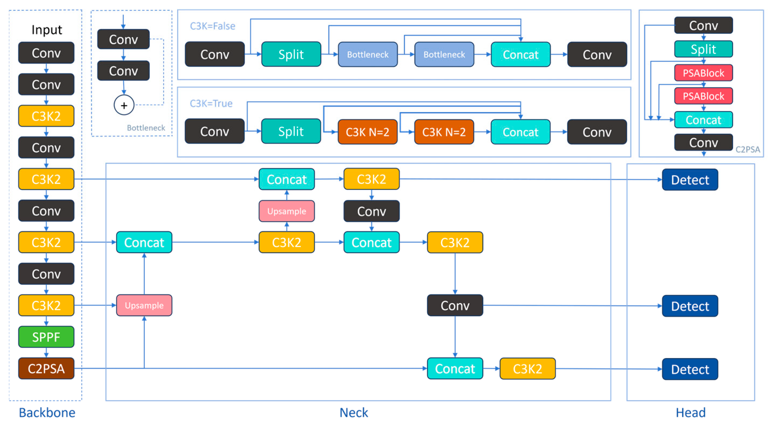
YOLOv11 is an object detection algorithm released by Ultralytics [
22]. Compared to older versions like YOLOv8, YOLOv11 has achieved significant breakthroughs in accuracy, speed, and efficiency, with core advantages in efficient feature extraction, lightweight real-time performance, multi-task compatibility, and dynamic adaptive capabilities [
20,
22,
23]. YOLOv11 continues the one-stage detection framework, allowing for the prediction of the categories and bounding boxes of all targets in an image via a single forward pass. The network structure includes the input layer (Input), backbone network (Backbone), neck network (Neck), and detection head (Head), as shown in
Figure 1.
The innovations of YOLOv11 compared to its predecessors such as YOLOv8 and v10 are mainly reflected in the following aspects: First, the YOLOv11 backbone network adopts an improved C3k2 (Cross Stage Partial with Kernel Size 2) module, which optimizes the convolutional kernel size and cross-stage connection method of the CSP (Cross Stage Partial Networks) structure to improve feature extraction efficiency while ensuring model stability. It connects two C3k sub-modules and dynamically switches to YOLOv8’s C2f structure, achieving adaptive balance between computational load and feature representation capability, thereby indirectly improving detection accuracy. Second, the neck network introduces the C2PSA module, innovatively fusing the CSP structure with Partial Self-attention (PSA) mechanism. This module can effectively enhance the model’s feature parsing capability for small targets and complex scenes, balancing detection accuracy and computational efficiency. Additionally, the Fast Spatial Pyramid Pooling (SPPF) layer is innovatively introduced, replacing the traditional Spatial Pyramid Pooling (SPP) structure. This structural design balances the advantages of multi-scale feature fusion and computational latency through a combination of serial and parallel pooling operations, further optimizing the model’s real-time inference performance. Meanwhile, YOLOv11 continues the design philosophy of YOLOv10 by embedding depthwise separable convolution into the detection head structure to reduce computational redundancy. This optimization strategy further improves computational efficiency while guaranteeing high model accuracy.
However, the YOLOv11 baseline model still has several issues to be optimized: In the backbone network design, although the C3k2 module is introduced and lightweight convolution replacement strategies are adopted to maintain efficiency, its representation capability for small-scale features remains insufficient. Second, the backbone network fails to adequately preserve target detail information during feature extraction, leading to limited multi-scale feature modeling capability and neck feature fusion capability. Furthermore, multiple downsampling processes result in a significant decrease in feature map resolution, and insufficient depth of multi-scale feature fusion makes the model’s recall rate and positioning accuracy for ultra-small targets (with extremely low pixel proportion) relatively low, with room for improvement in bounding box fitting accuracy.
2.2. ESI-YOLOv11n
In complex industrial scenario object detection tasks, traditional YOLO series models face three key bottlenecks: First, limited feature capture capability. Global context dependence is obtained through fixed pooling operations, leading to semantic information loss; local feature extraction relies on fixed-size convolution kernels, making it difficult to balance the effective utilization of multi-level features. Second, single feature interaction mechanisms. Insufficient modeling of inter-channel dependency relationships, lack of dynamic weight allocation in multi-scale feature fusion, making it difficult to balance effective utilization of different level features. Third, insufficient key information reinforcement. Lack of selective attention to target regions in complex backgrounds, highly susceptible to noise interference, leading to geometric constraint mismatches for irregular shapes, insufficient optimization capability for small targets and low overlap scenarios, and lower sensitivity to boundary details, especially limited performance in small target detection.
To address the problems existing in YOLOv11, this paper uses it as the baseline model to implement the following improvements:
Optimize the C3k2 module structure through Spatial-Channel Reconstruction Convolution (ScConv) to construct a dynamic feature perception unit, achieving efficient extraction of PCB defect features. This notably strengthens the perception capability of micro-features, reduces computational redundancy, and improves the model’s feature extraction capability in complex scenarios.
Embed the Efficient Multi-Scale Attention (EMA) mechanism into the subsequent layer of the C3k2 module in the Neck layer, dividing input features along the channel dimension into sub-feature groups with factor = 2, expanding the scale of single-group channels to retain more basic semantic information while maintaining computational efficiency, enhancing feature cross-scale fusion efficiency through adaptive weight allocation strategies, thereby improving model recall rate and detection performance.
Integrate the Inner constraint concept into the CIoU loss function to construct a geometric constraint regression mechanism adapted to small target characteristics, significantly improving the recall rate and positioning accuracy of small target detection through auxiliary frame positioning strategy and refined boundary fitting. Simultaneously, expand the channel dimension of the network’s hidden layers to twice that of the original structure, improving model generalization performance by increasing feature space capacity in scenarios with limited data scale, thus avoiding underfitting problems caused by insufficient parameters.
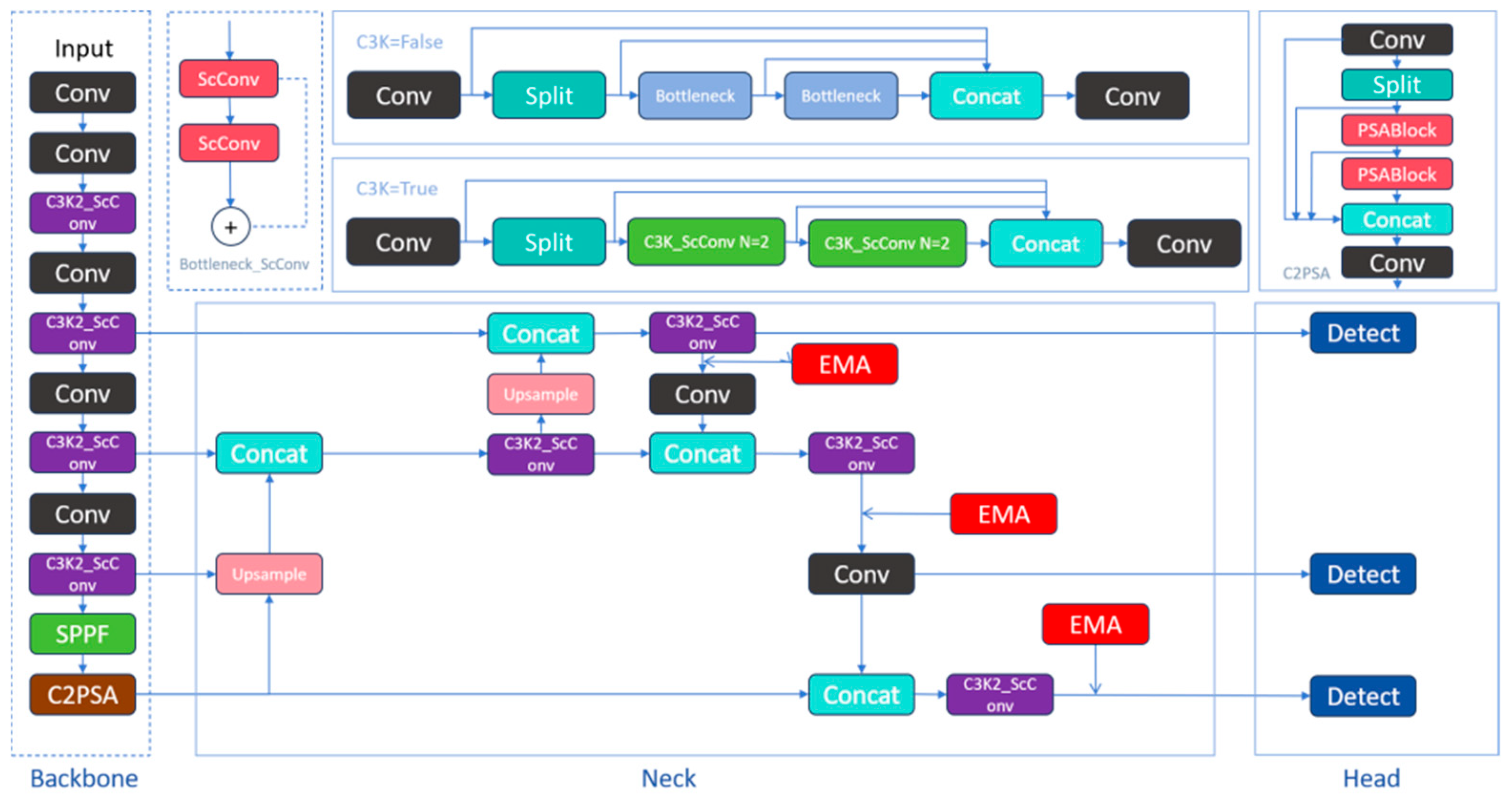
This improved model is named ESI-YOLOv11n. The targeted adjustment of its network structure, collaborative optimization of attention mechanisms, and auxiliary frame mechanism of loss functions provide a technical path for solving the difficulties of small target detection in industrial vision for PCBs. The improved model network structure is shown in
Figure 2.
2.2.1. Improved C3k2-ScConv Module
- 1.
ScConv Convolution Module
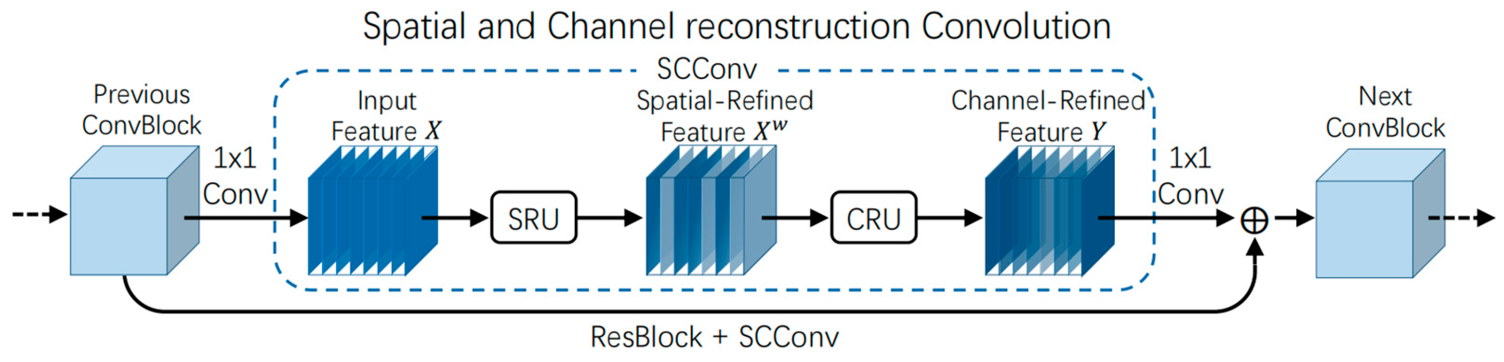
Convolutional neural networks excel in various computer vision tasks, but their efficient operation relies on substantial computational resources. The C3k2 module in YOLOv11 achieves comprehensive feature extraction by integrating multiple bottleneck modules but introduces significant channel information redundancy. Specifically, some channels exhibit high feature redundancy with other channels, resulting in redundant computations during forward propagation—these operations do not provide additional valid information but significantly increase memory overhead and computational complexity. To address these limitations, reduce resource overhead, improve target detection accuracy, and enhance feature representation capability, this paper introduces Spatial and Channel Reconstruction Convolution [
24] (ScConv) into the C3k2 module of YOLOv11 and carries out innovative improvements. Combining ScConv with the C3k2 module optimizes the feature extraction process while effectively reducing spatial and channel redundancy in convolutional neural networks, thereby achieving reductions in computational resource consumption and improvements in target detection accuracy. As shown in
Figure 3, ScConv includes two core units: the Spatial Reconstruction Unit (SRU) and the Channel Reconstruction Unit (CRU).
- 2.
Spatial Reconstruction Unit (SRU)
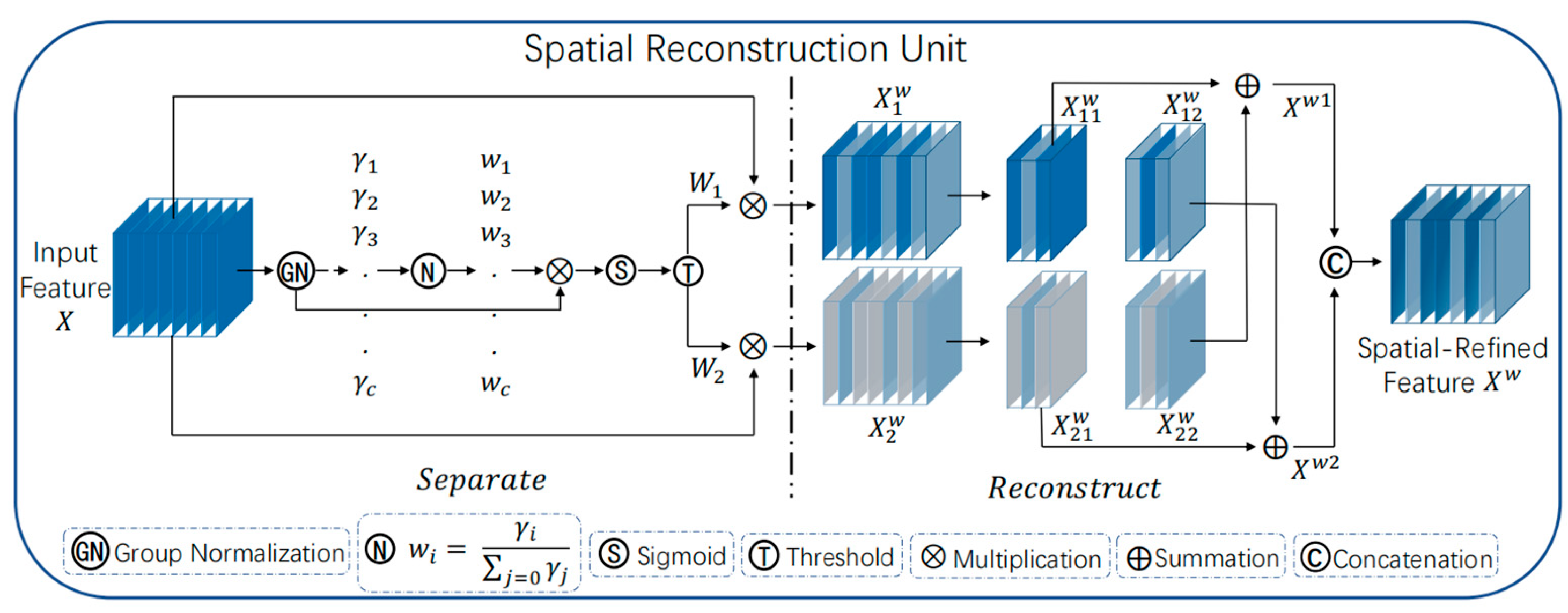
The Spatial Reconstruction Unit (SRU) serves as the core component of the ScConv module, functioning to reduce the spatial redundancy of input features through structured feature processing, thereby improving the feature processing efficiency of convolutional neural networks. Its structure is shown in
Figure 4.
The specific workflow of SRU is as follows:
Input feature preprocessing: Perform Group Normalization (GN) on the input feature map , eliminating scale differences between different feature maps through normalization operations to ensure numerical stability of subsequent operations.
Channel adaptive weighted separation: First, generate weights coefficients from the normalized feature map through a non-linear activation function; Then, based on this weight matrix, perform adaptive weighted operations on the channel dimension of the feature map, decoupling the original features into several semantic sub-feature sets.
Feature reconstruction: Split the weighted features into two parts, denoted as and , perform feature transformation on each, respectively, and finally accomplish feature reconstruction through additive fusion and channel concatenation, obtaining optimized spatial features with better semantic representation. The final computation process of the SRU module can be expressed as:
- 3.
Channel Reconstruction Unit (CRU)
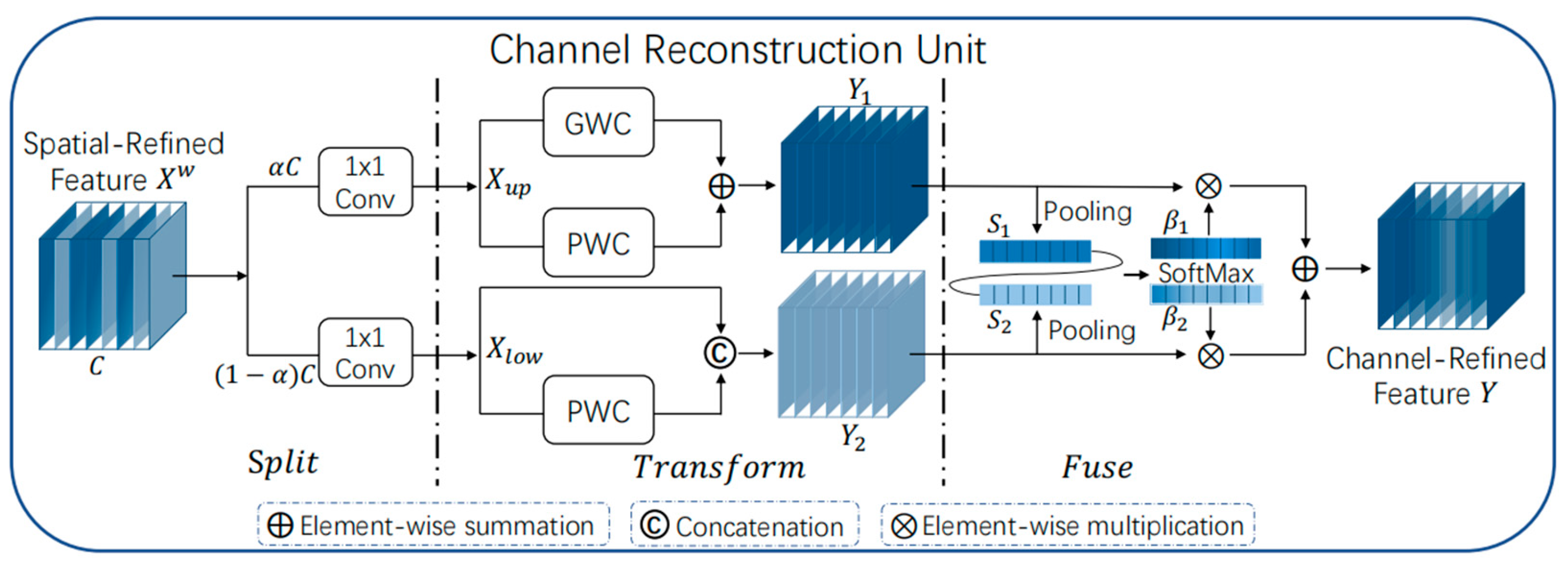
The Channel Reconstruction Unit (CRU) is the post-processing part of the ScConv convolution module, which aims to reduce channel redundancy in the network’s feature maps. CRU further performs channel splitting, transformation, and fusion operations on the spatial features
output after SRU processing, thereby more efficiently reducing channel redundancy and improving network model performance. Its structure is shown in
Figure 5.
The specific workflow of CRU is as follows:
Channel splitting: Divide the spatial features into two parts along the channel dimension, where α is the splitting ratio (0 < α < 1), and compress the number of feature map channels through 1 × 1 convolutions with different splitting ratios.
Transformation: Further transform the two parts of features and output via Group-wise Convolution (GWC) and Point-wise Convolution (PWC) instead of standard k × k convolutions.
Fusion: The two parts of features and after transformation undergo weighted fusion operations via pooling and SoftMax activation, forming the final channel-refined features . The final computation process of the CRU can be expressed as:
This structure uses a split-transform-fuse strategy to further reduce redundancy in the channel dimension of spatially refined feature maps. Additionally, CRU employs lightweight convolution operators for feature extraction and effectively reduces the model’s parameter count and computational cost.
- 4.
C3k2-ScConv
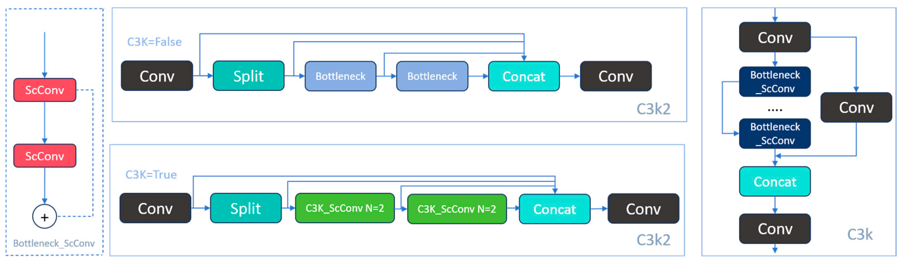
Based on the above advantages, this paper proposes embedding the ScConv module into YOLOv11’s C3k2 module, reconstructing the CSP structure through dynamic feature screening and multi-scale fusion mechanisms. By replacing the standard convolution layer in the traditional Bottleneck module with ScConv, leveraging the SRU’s adaptive channel-weighted separation and feature reorganization mechanisms, as well as CRU’s cross-scale information fusion operations, the C3k2 module is upgraded from a static convolutional structure to a dynamic feature processing unit. The C3k2-ScConv structure is shown in
Figure 6.
The C3k2-ScConv structure effectively reduces feature redundancy in both channel and spatial dimensions, significantly improving feature extraction capabilities in complex scenarios. However, in PCB small target defect detection, there are still issues with the easy loss of small-target features in high-level semantic representations and the difficulty in handling feature correlations in occluded scenarios. To address these issues, this paper proposes introducing the Multi-Scale Attention mechanism EMA to construct cross-scale semantic interaction channels and a global context-aware module to strengthen information flow between different scale features, enhancing the model’s robustness for small targets and occlusion scenarios, providing a better feature representation foundation for precise PCB defect detection.
2.2.2. EMA Mechanism
Attention mechanisms [
25] serve as core supporting technologies in machine learning research, which dynamically assigns weights to different regions of input features, enabling the model to focus on key information and suppress redundant features, effectively improving robustness and generalization capabilities. Classic attention mechanisms such as the Squeeze-and-Excitation Module (SE) [
26] and Convolutional Block Attention Module (CBAM) [
27] achieve attention weight calibration in channel dimensions and channel-spatial dual dimensions, respectively, but their complex computation processes lead to relatively high time overhead. This paper introduces the Efficient Multi-Scale Attention (EMA) module [
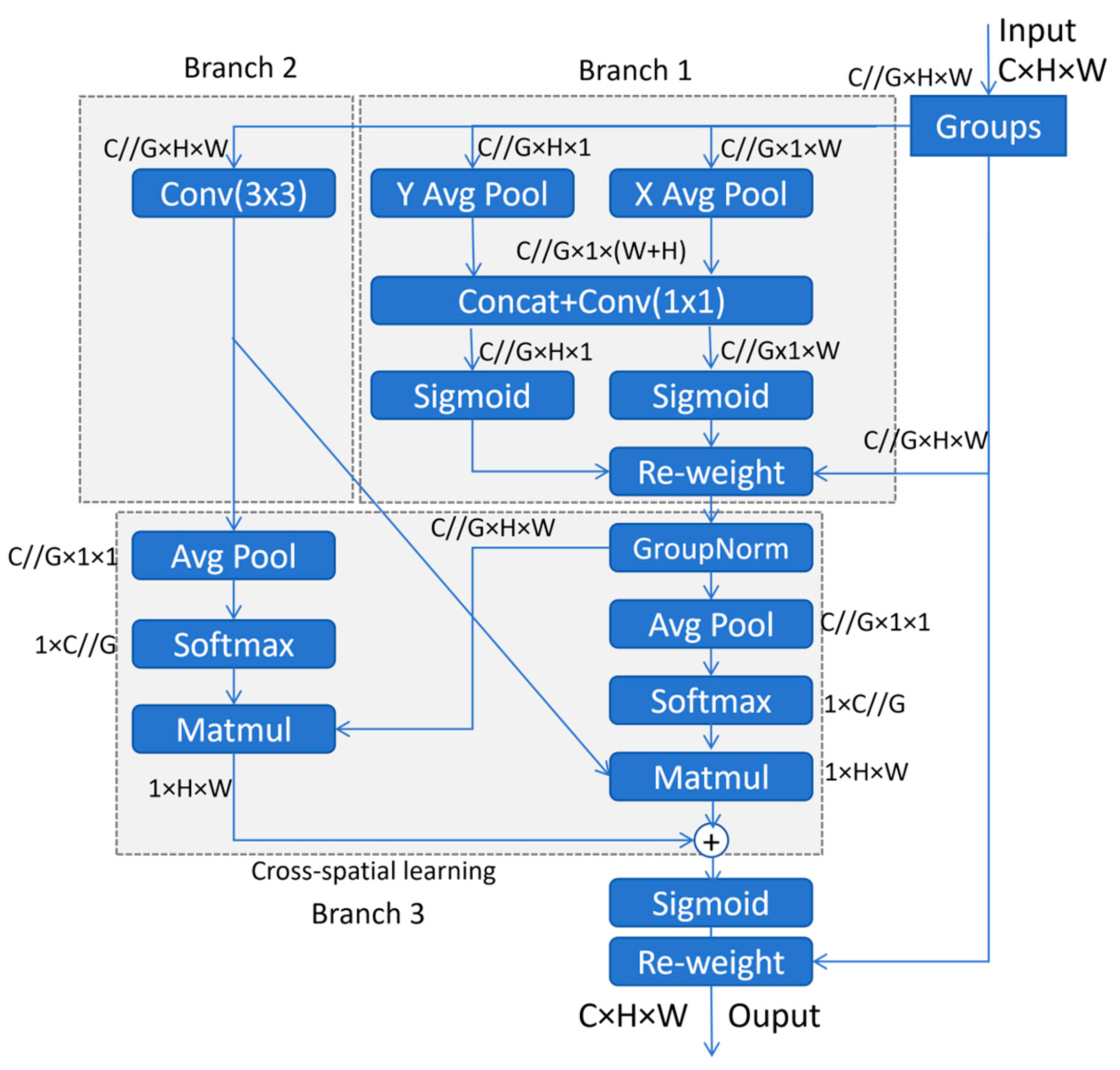
28], achieving a balance between accuracy and efficiency through a hybrid-domain attention mechanism. EMA is a lightweight multi-scale attention module whose core concept is to optimize features without reducing channel dimensions by means of channel grouping, parallel multi-scale convolution, and cross-dimensional interaction. This mechanism avoids information loss caused by dimensionality reduction in traditional attention modules and achieves collaborative feature enhancement through three parallel branches: 1) Coordinate attention branch: The original input feature tensor
(batch size B, number of channels C, spatial dimensions H × W) is first evenly divided along the channel dimension to form G independent channel subgroups, each containing
=
C/G feature channels, resulting in
. Horizontal average pooling (X Avg Pool) and vertical average pooling (Y Avg Pool) are applied to each subgroup to capture global contextual information in the horizontal and vertical directions. The pooling results are concatenated (Concat) and then compressed along the channel dimension via 1 × 1 convolution, followed by Sigmoid activation to generate coordinate attention weights, achieving channel-level reweighting of the original grouped features and enhancing the semantic representation of key channels. This process can be expressed as:
In the formula: is the output feature after horizontal average pooling, is the output feature after vertical average pooling, represents the input feature, H and W represent height and width,, respectively, i and j represent indices respectively; σ is Sigmoid activation, ⊙ is element-wise multiplication, Conv1 represents convolution operation.
Local feature branch: It uses
convolution to extract local spatial features, enhancing the expression local detail via Sigmoid activation to compensate for fine-grained information potentially lost in global attention. This process can be expressed as:
In the formula, , represents the sub-channel features, represents convolution operation.
Normalization and interaction branch: Grouped features first undergo Group Normalization to eliminate discrepancies in data distribution and extract statistical features via global average pooling. Spatial feature interaction is achieved via Softmax and matrix multiplication (Matmul), mining cross-position dependencies, and finally achieves spatial attention calibration via Sigmoid activation and weight adjustment. Ultimately, the outputs of the three branches undergo cross-dimensional fusion via multi-round weight redistribution, ultimately generating optimized feature maps with the same dimensions (
H × W × C) as the input. This process can be expressed as:
In the formulas: denotes the output features of the normalization operation, denotes the normalization operation, denotes the grouped feature maps, ⊙ represents element-wise multiplication, denotes spatial weights; denotes the global average of the feature map for channel C, denotes the average operation, and respectively denote summation over height and width dimensions, xc(i,j) denotes the feature value of channel C at position ; denotes the generated global attention weights, Softmax denotes the application of the Softmax function to convert the input into a probability distribution, denotes flattening multi-dimensional feature maps into one-dimensional vectors; EMA denotes the features generated by the attention mechanism, denotes the module’s input features, denotes reshape operation, denotes grouping operation, denotes the application of the Sigmoid activation function, represents element-wise multiplication.
With only a 1.2% increase in computational overhead, this module significantly enhances the model’s detection capability for small and medium targets and semantically ambiguous targets in complex scenarios [
29]. In the improved YOLOv11 network, the structure of the EMA module is shown in
Figure 7 (where
C,
H, and
W represent the number of channels, height, and width respectively, and G represents the number of sub-feature groups). Its innovative grouping strategy and lightweight interaction mechanism provide an effective solution for YOLO series algorithms to break through the detection accuracy bottlenecks while maintaining real-time inference performance.
2.2.3. Inner-CIoU Loss Function
Bounding box regression serves as a core step in small target detection tasks, and its prediction accuracy directly determines the final performance of target detection. However, the CIoU [
30] bounding box regression loss function used in current YOLO algorithms has inherent limitations in the special scenarios of PCB small-target defect detection: CIoU exhibits mismatched geometric constraints for irregular defect shapes, inadequate optimization for small targets and low-overlap scenarios, and low sensitivity to boundary details. When the predicted bounding box has the same aspect ratio as the ground-truth box but differs in specific dimensions, it fails to effectively guide the model’s optimization direction. Therefore, this paper incorporates the Inner-IoU concept to improve the CIoU loss function, resulting in the Inner-CIoU [
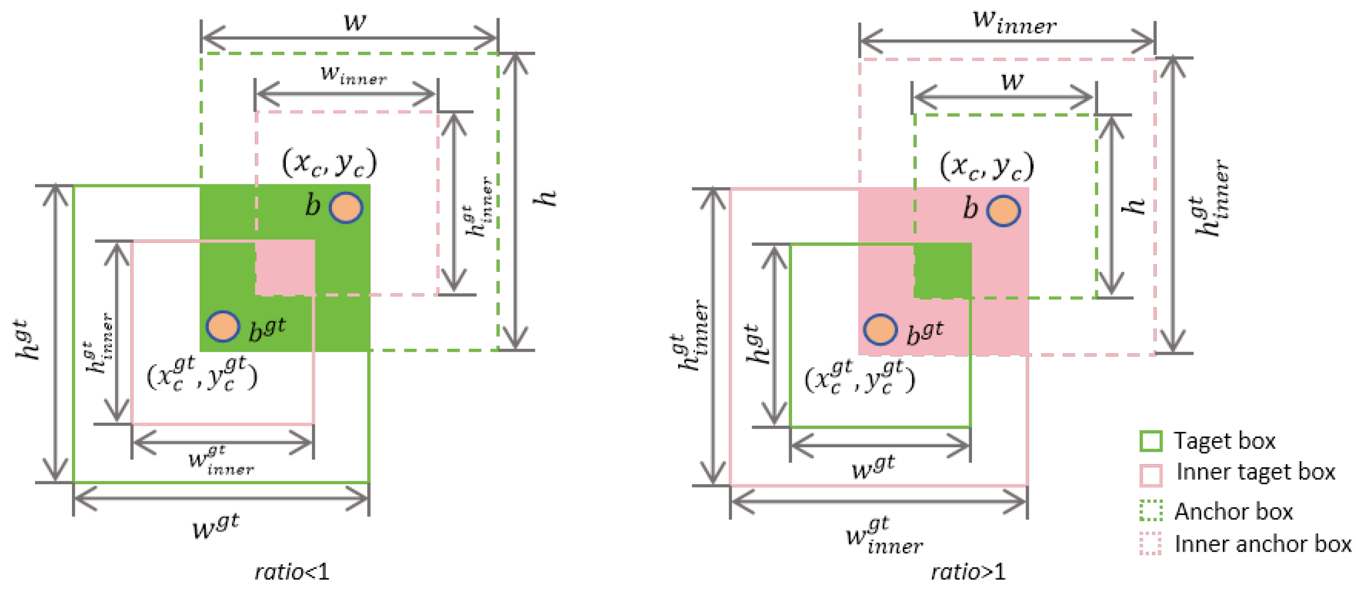
31] loss function. Based on CIoU, auxiliary bounding boxes are introduced, composite loss functions are constructed via Inner-IoU calculation, and a parameterized control mechanism is adopted to adjust the geometric dimensions of the auxiliary bounding boxes, enabling the detection models to adapt to different data distribution characteristics. The Inner-IoU structure is shown in
Figure 8.
In
Figure 8, the ground-truth box and the predicted box are denoted as
and
b respectively, the center points of the ground-truth box and the auxiliary ground-truth box are denoted as
, the center points of the predicted box and auxiliary predicted box are denoted as (
,
), the width and height of the ground-truth box are denoted as
and
respectively, and the width and height of the predicted box are denoted as
w and
h respectively. The scale factor is denoted as ratio, with its range constrained to 0.5–1.5. The definition of Inner-IoU can be expressed by Equations (11)–(15):
The auxiliary boxes bl, br, bt, and bb are also defined for the predicted box with the same ratio value. Thus,
The Inner-IoU loss function retains key characteristics of the IoU loss function. Experimental results show that when this loss function is adopted, Inner-IoU exhibits better convergence in low IoU scenarios when
> 1, as the introduction of large-scale auxiliary bounding boxes effectively expands the model’s detection range; when
< 1, Inner-IoU reduces the effective regression range and yields a smaller loss value than IoU, yet it exhibits better convergence in high-IoU sample scenarios. Therefore, IoU and Inner-IoU differ only in scale, with identical loss calculation methods. Based on the definition of the CIoU loss function, the Inner-CIoU loss function is defined as follows:
2.3. Module Layout Design and Key Parameters
Although YOLOv11 represents a significant innovation compared to predecessors such as YOLOv8 and v10, it inherently exhibits distinct deficiencies in feature extraction and detection effectiveness for tiny targets. To address this, the module layout design of the ESI-YOLOv11n model proposed in this paper strictly adheres to the core principles of layer-level functional adaptation, targeted breakthrough of pain points, and synergistic module enhancement. Based on the composite scaling parameters [0.50, 0.25, 1024] of the YOLOv11n model (scale = ‘n’), and leveraging the three core components of the original network (Backbone, Neck, and Head), this design addresses the core pain points of PCB defect detection. These pain points include weak tiny-target features, inefficient multi-scale feature fusion, insufficient small-target positioning accuracy, and underfitting caused by limited data scale. The improved modules are precisely laid out according to the specific structural configuration of the model:
Backbone feature extraction layer: ScConv is embedded into the C3k2 modules of layers 2, 4, 6, and 8 to construct the C3k2-ScConv structure. This optimizes the C3k2 module structure and establishes a dynamic feature perception unit. Combined with the progressive channel design of the Conv modules in the Backbone, this design enables efficient extraction of multi-scale PCB defect features. This design specifically enhances the perception of micro-features and reduces computational redundancy, while satisfying lightweight requirements and improving feature extraction performance in complex scenarios.
Neck feature fusion layer (integrated within the Head structure): Strictly following the model configuration, the EMA mechanism is embedded after the C3k2-ScConv modules corresponding to the P3, P4, and P5 scales (layers 16, 19, and 22). The parameter factor is set to 2 to divide the input features into subgroups along the channel dimension. This expands the channel scale of each subgroup while maintaining computational efficiency, thus preserving more basic semantic information. Adaptive weight allocation strategies enhance the cross-scale fusion efficiency of multi-scale features, thereby improving the model’s recall rate and detection performance. Ultimately, it cooperates with the Detect layer for the fusion detection of P3, P4, and P5 scale features, achieving comprehensive coverage of multi-scale defects.
Head detection output layer: The Inner-IoU constraint concept is integrated into the CIoU loss function to construct a geometric constraint regression mechanism tailored to small-target characteristics. Via auxiliary box positioning and refined boundary fitting, the recall rate and positioning accuracy of small-target detection are significantly improved. Meanwhile, combined with a channel expansion design, the channel dimension of the network’s hidden layers is expanded to twice that of the original structure. Corresponding to the channel configurations (512, 1024, 2048) of the C3k2-ScConv modules in the Backbone and Head, this design increases the feature space capacity under limited data scale, enhancing the model’s generalization performance and avoiding underfitting caused by insufficient model parameters.
The layout of all improved modules and the channel expansion strategy are strictly aligned with the model’s structural configuration, synergistically forming a closed loop of feature extraction-feature fusion-detection output-generalization guarantee. This enables the deep adaptation of each module’s function to the core positioning of its corresponding layer while balancing model lightweightness (adhering to requirements, the parameter constraints of the ‘n’ scale parameters) and industrial application needs, thus providing a scientific and reasonable architectural foundation for the comprehensive improvement of the model’s detection performance. Key parameters are summarized in
Table 1.
3. Experiments
3.1. Dataset
This paper adopts the PKU-Market-PCB public dataset [
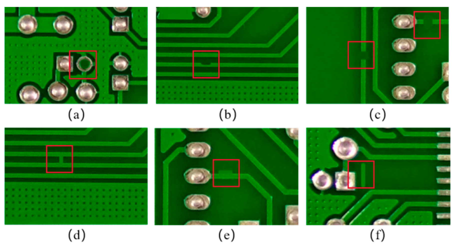
32] from the Peking University Laboratory, containing 693 images with six typical PCB defects: Missing hole, Mouse bite, Open circuit, Short, Spur, and Spurious copper. The initial sample distribution of each category is balanced, as illustrated in
Figure 9.
To enhance the model’s generalization ability and alleviate the small-sample learning problem, this study implements multi-dimensional data augmentation strategies, as detailed below:
Basic preprocessing: Median filtering denoising, normalization (pixel values mapped to the [0, 1] interval), and adaptive brightness adjustment are sequentially applied to the original images to eliminate imaging noise and lighting differences.
Geometric transformation enhancement: Random rotation operations within a ±10° range are used to expand the sample space, with blank areas uniformly filled with black pixel values to avoid introducing pseudo-feature interference. Through the aforementioned processing, the dataset scale is expanded from the original 693 images to 1386 images, as presented in
Table 2.
According to the standard data division specifications in the industrial inspection field, this study strictly partitions the complete dataset into a training set, a validation set, and a test set at a ratio of 7:2:1. During the division process, stratified random sampling is employed to ensure that the class distribution of each subset is consistent with that of the original dataset, thereby avoiding the adverse impact of class imbalance on experimental results. This dataset construction scheme provides a reliable data foundation for subsequent model training and performance evaluation.
3.2. Experiment Setup
All experiments in this paper are conducted based on a unified software and hardware environment, with the detailed configuration presented in
Table 3. The hardware platform is equipped with an NVIDIA RTX 4090 GPU (24 GB memory), paired with an Intel i9-13900K CPU and 64 GB memory, which provides sufficient computational support for large-scale data processing and model training. The software environment is built based on the PyTorch 2.5.0 framework, equipped with CUDA 12.4 and the Windows 11 operating system, ensuring the efficiency and compatibility of algorithm implementation.
The detailed experimental parameter settings are listed in
Table 4, primarily including the hyperparameter configuration for model training and the specific data processing strategies. The training process adopts the AdamW optimizer, with the initial learning rate set to 0.008, and integrates the cosine annealing learning rate decay strategy (Cosine Annealing LR Scheduler) for dynamic learning rate adjustment, aiming to balance convergence speed and optimization accuracy. The batch size is set to 16, the input image resolution is uniformly adjusted to 640 × 640 pixels to meet model input requirements, and the training epochs are set to 400. Data augmentation strategies include random rotation, contrast enhancement, and brightness adjustment, which further improve the model’s generalization ability.
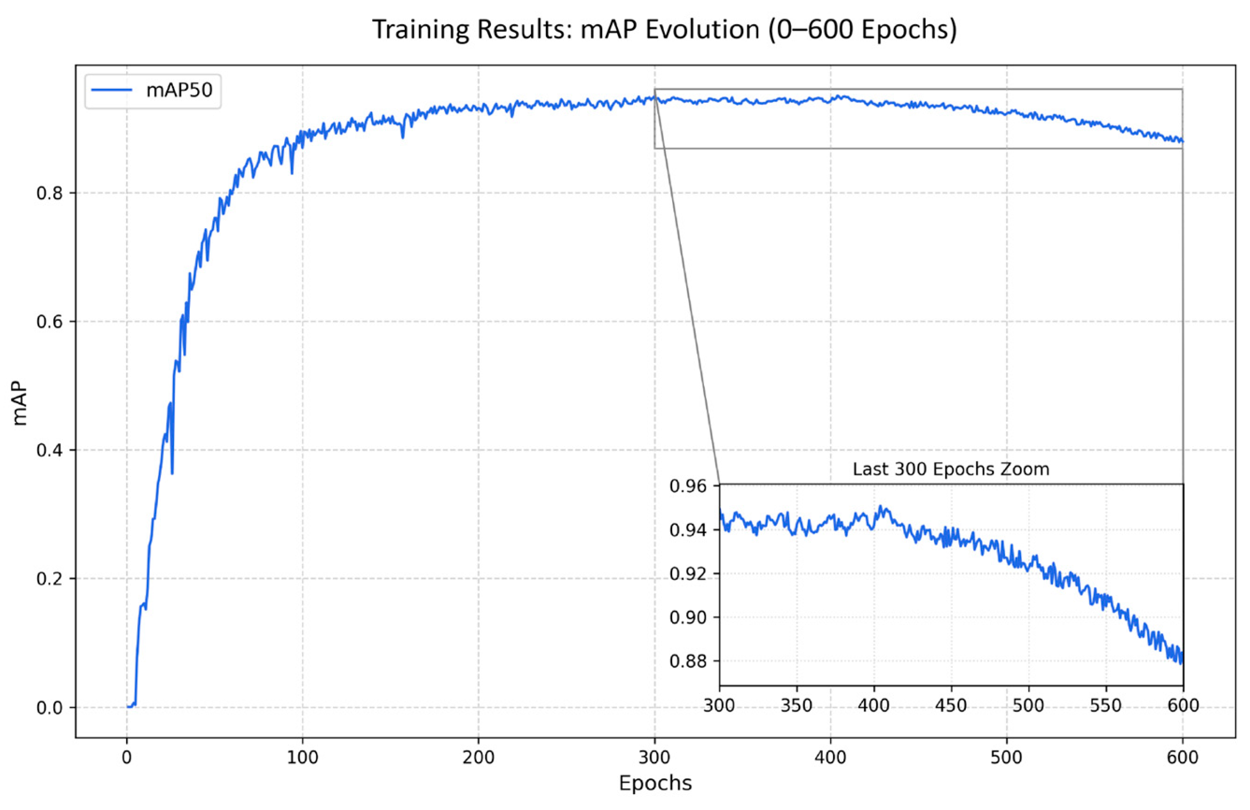
Based on the characteristics of the limited PCB defect dataset, this study designates 400 training epochs as the core training node. To demonstrate the rationality of selecting 400 epochs for a limited dataset, the model was trained for 100, 200, 300, 400, 500, and 600 epochs respectively. As demonstrated by the 600-epoch training result curve, 400 epochs fully cover the complete process from feature learning and stable convergence to performance fine-tuning. This aligns with the training dynamics characteristic of limited datasets, enabling full exploitation of data features while avoiding underfitting caused by insufficient training. Furthermore, the model avoids the overfitting phase where performance rapidly degrades; the training curve shows that at 400 epochs, the mAP remains stable without significant decline, resulting in controllable overfitting risk. Simultaneously, this training duration avoids the ineffective training phase with extremely low marginal gains, balancing training efficiency and effectiveness while ensuring stable generalization performance. The scientific validity and adaptability of this configuration to limited dataset scenarios are further supported by synchronous monitoring of validation metrics and the integration of anti-overfitting measures such as data augmentation. The mAP@50 results of the 600-epoch training are illustrated in
Figure 10.
3.3. Evaluation Metrics
This paper adopts multi-dimensional metrics to evaluate the model performance, including Precision (P), Recall (R), Mean Average Precision (mAP), F1 score, and Giga Floating-point Operations Per Second (GFLOPs). The mathematical definitions of each metric are shown in Formulas (17) to (21).
Formula (17) defines Precision, which measures the proportion of samples that truly belong to positive categories among samples predicted as positive by the model. This metric quantifies the credibility of effective predictions in detection results and directly reflects the reliability of the model’s prediction outcomes; where TP is true positive (correctly detected defect samples), and FP is false positive (normal samples misclassified as defects).
Formula (18) defines Recall (R), which measures the proportion of real defects that are correctly detected, reflecting the model’s ability to capture defects (i.e., “recall rate”), where FN is false negative (missed defect samples).
Formula (19) is the core evaluation metric for object detection tasks, comprehensively reflecting the model’s detection capability for multi-category defects by calculating the Average Precision (AP) of the 6 defect categories at different Intersection over Union (IoU) thresholds and then taking the average value. In the formula, Nc represents the total number of target categories in the dataset, 50 and 0.50 indicate the values at an IoU threshold of 0.50, and in , AP refers to the Average Precision of the k-th category target at IoU threshold of 0.5, which is used to measure the model’s detection accuracy for that specific category. This metric simultaneously considers detection box positioning accuracy and classification accuracy, serving as the key basis for evaluating the model’s generalization ability in PCB defect detection tasks.
Formula (20) defines the F1 score, which is the harmonic mean of Precision and Recall, balancing the performance trade-off between the two metrics and is suitable for comprehensive evaluation in imbalanced category scenarios.
Formula (21) defines GFLOPs (Floating-point operations er Second), which represents the number of floating-point operations required for the model to process a single image (unit: billion times) and is used to quantify the computational complexity of the model. converts the total floating-point operations to billions for intuitive representation of operations per second; the summation symbol sums over the L layers of the model, accumulating the floating-point amount for each layer; and are the height and width of the -th layer feature map; is the input channel number of the -th layer, determining input feature dimensions; represents the convolution kernel area of the -th layer; and represents the output channel of the -th layer. This metric directly affects the feasibility of algorithm deployment on edge devices or in real-time detection scenarios—the smaller the GFLOPs, the higher the model’s inference efficiency.
The above metrics construct a comprehensive evaluation system from three dimensions: detection accuracy, robustness, and engineering practicality, ensuring that the model not only possesses excellent detection capability for PCB defects (especially small targets) but also meets the computational efficiency requirements of practical applications.
3.4. ESI-YOLOv11n Loss Function Curve
The loss function is the core guide for deep learning model optimization, and its dynamic changes directly reflect the model’s fitting degree to the target task. In PCB defect detection, a typical small target detection task, the loss function quantifies the deviation between the prediction results and the ground truth labels, providing gradient directions for model parameter updates and serving as a key metric for evaluating training stability and optimization effectiveness. This paper adopts a multi-task joint loss function, including bounding box regression loss (box_loss), classification loss (cls_loss), and distribution focal loss (dfl_loss), which correspond to positioning accuracy, category discrimination ability, and probability distribution optimization in object detection tasks, respectively.
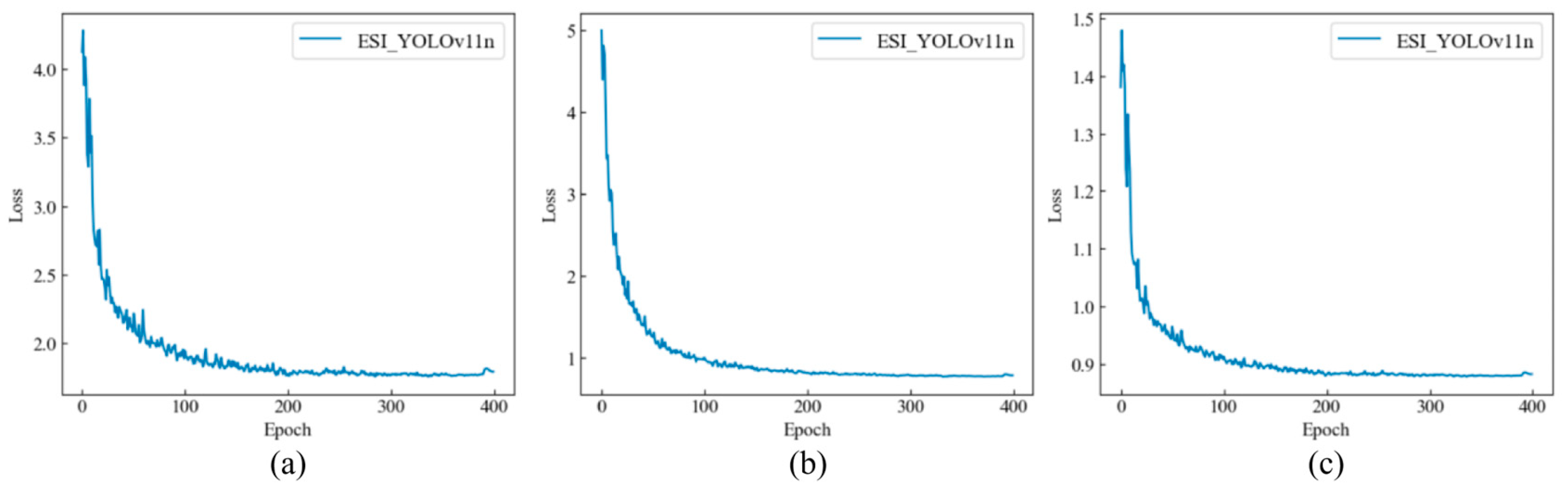
Figure 11 shows the variation curves and scatter distributions of the three types of loss functions on the validation set with training epochs, where the horizontal axis represents training epochs (1–400 Epoch), and the vertical axis represents normalized loss values (Loss).
Figure 11a shows the variation curve of bounding box regression loss (val/box_loss) with training epochs. Box_loss is used to optimize the positional deviation between predicted boxes and ground truth boxes, with Inner-CIoU Loss as the core metric. In the early training stage, the loss value rapidly decreases from a high level, reflecting the precise constraint of Inner-CIoU Loss on the boundary point distance between predicted boxes and ground truth boxes, which provides effective gradients even in non-overlapping or low-overlapping scenarios, guiding the model to quickly learn the precise alignment of defect boundaries. As training progresses, the decline rate slows down, the loss stabilizes after 150 epochs and finally stabilizes in the low range of 1.4–1.5 after 250 epochs, indicating that the model’s positioning accuracy for PCB defect bounding boxes gradually improves and converges. This effectively solves the shortcomings of traditional loss functions in the positioning of complex PCB defects (such as micro short circuits, irregular pad missing) and strengthens the regression of boundary details.
Figure 11b shows the variation curve of classification loss (val/cls_loss) with training epochs. In the early training stage, the loss value decreases significantly, reflecting the model’s rapid learning of discriminative features for different defect categories, with its recognition ability for various defect types (such as short circuits and open circuits) improving rapidly. As training progresses, the decline rate slows down, fluctuations become smaller around 100 epochs, and the loss gradually stabilizes at a low value around 0.6, indicating that the model’s classification confidence for the six defect categories gradually strengthens. This effectively suppresses background noise interference, improves classification accuracy, and ensures the accurate identification of defect categories in complex PCB backgrounds.
Figure 11c shows the variation curve of distribution focal loss (val/dfl_loss) with training epochs. Dfl_loss addresses positioning deviation caused by probability distribution discretization in small target detection by modeling the continuous probability distribution of bounding box coordinates to improve regression accuracy. The loss sharply decreases in the initial stage; the decline rate slows but continues to optimize in the middle stage (about 50–150 epochs) and finally stabilizes around 0.7. This indicates that the model significantly enhances its regression capability for defect positions through distribution optimization, with particularly obvious effects when handling small-sized or distributionally complex defects. This loss optimizes the distribution characteristics of position regression, enabling the model to more precisely locate defects in PCB defect detection. Even when facing tiny or specially shaped defects, it improves positioning accuracy through the guidance of distribution focal loss, providing more reliable position information for subsequent detection tasks.
Comprehensively analyzing
Figure 11a–c, all three loss curves show a trend of “rapid decline first, then stable convergence”, with no violent oscillations during the training process, which validates the stability and effectiveness of the model training in this paper. The loss value remains low and stable after 200 epochs, indicating that the model has fully learned the characteristics of PCB defect data, with neither overfitting (loss remains low without abnormal fluctuations) nor underfitting (loss does not stagnate at high levels). This thus provides a guarantee for the model to achieve reliable and accurate detection performance in PCB defect detection.
3.5. Ablation Experiments
To verify the effectiveness of the proposed method in this paper, ablation experiments were designed on the benchmark dataset, comparing the performance of the original YOLOv11n model with that of the improved ESI-YOLOv11n architecture proposed in this study. The comparison experiment results are shown in
Table 5.
Based on the quantitative results in
Table 5, this paper verifies the synergistic optimization effects of the EMA mechanism, C3k2-ScConv structure, and Inner-CIoU loss function through modular superposition experiments, with specific performances as follows:
After embedding the EMA mechanism into the YOLOv11n baseline model, precision (P) improves by 1.9%, recall (R) improves by 10.3%, validating that EMA enhances feature discriminability through dynamic weight allocation; mAP@0.50 improves by 8.1%, mAP@0.5:0.95 improves by 7.3%, indicating the effectiveness of global context modeling for multi-scale defect detection; although the computational overhead increases somewhat, the model still maintains lightweight characteristics.
After simultaneously superimposing EMA and C3k2-ScConv on the YOLOv11n baseline model, P reaches 95.2% (cumulative improvement of 2.1% over the baseline), R reaches 92.4% (cumulative improvement of 10.6%), showing the gain of dynamic feature reconstruction for small target feature extraction; mAP@0.50 reaches 95.3% (cumulative improvement of 8.7%), mAP@0.5:0.95 improves to 52.1% (cumulative improvement of 8.3%), validating the complementary effects of multi-scale feature fusion and channel decoupling.
After integrating EMA, C3k2-ScConv, and Inner-CIoU on the YOLOv11n baseline model, P and R improve by 2.4% and 11.5% respectively compared to the baseline, mAP@0.50 improves by 9.3%, mAP@0.5:0.95 improves by 8.7%; F1 score improves by 7.2%, indicating the balanced optimization of precision and recall; although GFLOPs increase relatively, the model size remains at 13.3 Mb, and the model’s detection efficiency still meets the real-time requirements of industrial applications.
The results show that the three modules (EMA, C3k2-ScConv, and Inner-CIoU) improve model detection performance from three dimensions: “feature weight allocation”, “multi-scale feature reconstruction”, and “positioning geometric optimization” respectively, with super-linear synergy effects when the three are fused. In addition, the improved model achieves a balance between detection accuracy and real-time performance while maintaining lightweight characteristics, providing an efficient solution for industrial online PCB defect detection.
3.6. Performance Comparison and Analysis
3.6.1. Experimental Configuration
To ensure consistency and precision in the experimental setup, a desktop GPU platform typical of industrial scenarios was selected for testing. The experimental environment remained consistent throughout (input image size is 640 times 640, batch size = 1, and non-deterministic operators disabled): Desktop GPU: NVIDIA RTX 3090 (CUDA 11.6, cuDNN 8.4), which is primarily used to verify real-time performance in medium-computing-power scenarios.
3.6.2. Evaluation Metrics
Frame Rate (FPS): The number of image detections completed per unit of time, reflecting the real-time detection capability of the model;
Time per Frame (ms): The average time elapsed from inputting a single image to outputting the detection result, calculated as the reciprocal of the frame rate;
Peak Memory Usage (MB): The maximum memory occupation of the GPU or edge device during the inference process, reflecting the resource requirements for model deployment;
GFLOPs: Theoretical floating-point operations (109 operations), reflecting the theoretical computational complexity of the model.
3.6.3. Performance Results and Analysis
As indicated in
Table 6, although ESI-YOLOv11n exhibits an increase in computational metrics compared to the original baseline model, it fully satisfies the real-time requirements for industrial online PCB detection based on industrial minimum standards (FPS ≥ 25, single-frame latency ≤ 40 ms):
In terms of real-time performance, ESI-YOLOv11n achieves an inference frame rate of 88.8 FPS on medium-computing-power devices, with a single-frame latency of 11.26 ± 1.41 ms. This performance is far above the real-time threshold for online detection on PCB production lines (typically requiring FPS ≥ 25 and latency ≤ 40 ms). This result validates the model’s efficiency in continuous detection scenarios, demonstrating its ability to stably adapt to the rhythmic flow of industrial production lines.
From the perspective of computing power adaptability, the peak memory usage of ESI-YOLOv11n is only 136.2 MB, with a floating-point operation count of 24.9 GFLOPs. This resource demand falls well within the carrying capacity of medium-computing-power devices (such as the NVIDIA Jetson Nano or entry-level GPUs), enabling deployment without reliance on high-cost hardware and meeting industrial needs for low cost and high availability.
Regarding the core design positioning, ESI-YOLOv11n follows an optimization logic of “prioritizing precision under medium computing power.” Compared to the baseline YOLOv11n, the model introduces modules such as ScConv dynamic feature extraction, EMA multi-scale attention fusion, and Inner-CIoU small target regression. While this results in a moderate increase in computational load (GFLOPs increasing from 6.3 to 24.9), it significantly enhances the detection accuracy for tiny PCB defects (e.g., pinholes, shallow scratches), directly addressing the core pain point of “high missed and false detection rates” in industrial quality inspection. This trade-off between “precision priority and efficiency adaptation” ensures practical value in industrial scenarios without exceeding the resource constraints of medium-power devices, providing a feasible technical path for the intelligent upgrade of PCB production lines.
In summary, the performance of ESI-YOLOv11n aligns highly with industrial real-time monitoring requirements. Its design positioning of “prioritizing precision under medium computing power” achieves an engineering balance between detection accuracy and deployment efficiency, demonstrating significant potential for industrial application.
3.7. Comparative Experiments
3.7.1. Comparison of Different Attention Mechanisms
To verify the effectiveness of the multi-scale fusion attention mechanism in PCB defect detection, comparative experiments were conducted based on the YOLOv11n baseline model. Mainstream attention mechanisms were selected for comparison, including the classic hybrid attention mechanism CBAM (Convolutional Block Attention Module), the pure channel attention mechanism CA (Channel Attention), and the large kernel attention mechanism LSKA (Large Kernel Attention). All attention mechanisms were embedded into the neck feature fusion network of YOLOv11n to construct corresponding models. The detection performance of each model on PCB defects is shown in
Table 7.
As can be seen from
Table 7, the integration of the EMA attention module in the YOLOv11n neck network significantly enhances the model’s defect detection capability. The specific performances are as follows:
After integrating the EMA attention module into the Neck layer, the improved model’s average precision mAP@0.50 increases from 86.6% of the baseline model to 94.7%, an increase of 8.1 percentage points, validating EMA’s precise positioning capability for multi-scale defect targets. This improvement is significantly higher than CBAM (+6.8%), CA (+6.3%), iEMA (+3.5%), and LSKA (+1.5%), highlighting EMA’s superiority in cross-scale feature fusion.
The model’s precision (P) reaches 95.0%, recall (R) reaches 92.1%, improving by 1.9% and 10.3% respectively compared to the original model. This indicates that the model can effectively reduce false positives in non-defect areas and significantly enhance the capture capability for micro defects.
3.7.2. Comparison with Baseline Model YOLOv11n
- 1.
Comparison of Indicators for Various Defects
As shown in
Table 8, compared with the baseline model YOLOv11n, the improved model shows significant improvements in the detection of mouse bites, open circuits, spurs, and spurious copper defects, with AP values all exhibiting substantial increases, confirming that the model’s ability to capture PCB micro defects has been enhanced, especially for defect types that previously demonstrated moderate performance.
- 2.
Comparison of Recall Rate and mAP@0.5 Curves Before and After Improvement
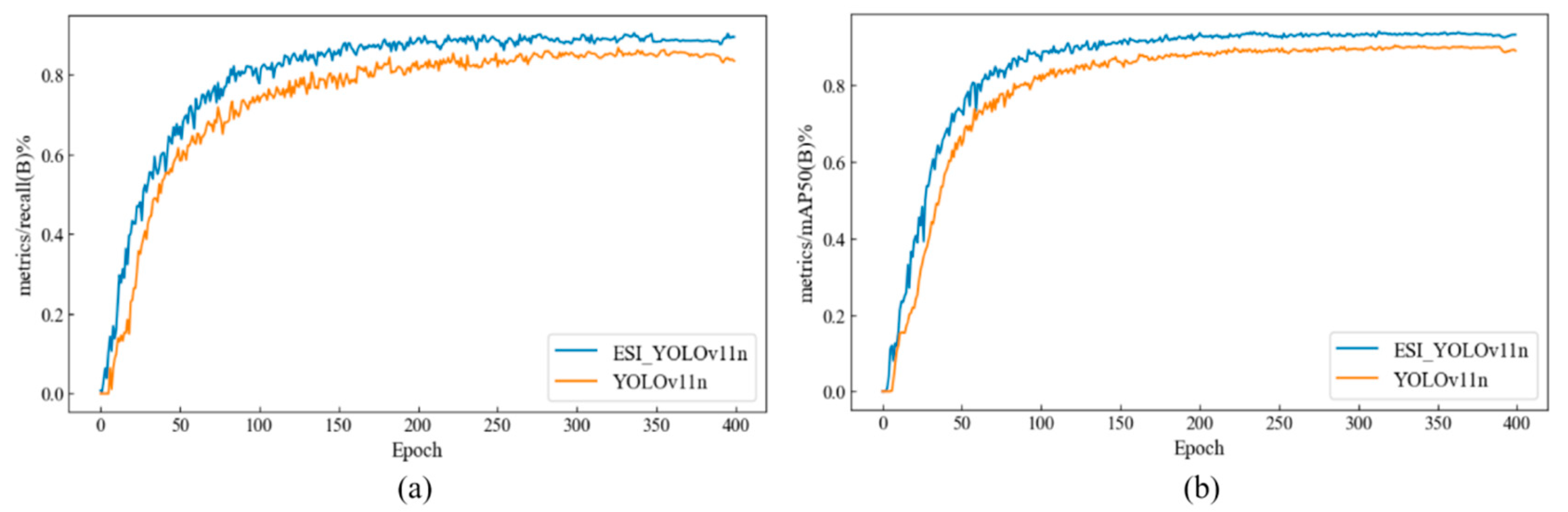
Figure 12 shows the comparison of mAP@0.5 and recall rate R curves before and after model improvement in this paper. The yellow line represents the indicators of the original model, and the blue line represents those of the improved model. As can be seen from
Figure 12, the improved model not only shows significant improvements in both recall rate and mAP@0.5 indicators, but also accelerates the convergence speed, thus comprehensively improving the model’s detection accuracy and performance.
3.7.3. Comparison of Different Detection Algorithms
To further validate the superiority of the proposed algorithm, this paper selects representative models covering traditional two-stage detection, one-stage detection, and the YOLO series for comparative experiments, including Faster-RCNN, SSD, RT-DETR [
33], YOLOv5, v6, v8, v9, and v10. The experimental results are shown in
Table 9.
Based on the experimental results, the proposed ESI-YOLOv11n algorithm demonstrates the best comprehensive performance in PCB defect detection. Its core metrics, including precision (P), recall (R), and mAP, are significantly superior to those of other models, making it highly suitable for industrial scenarios with extremely stringent requirements for detection accuracy. Although the computational cost of the model is slightly higher than that of some other models, its computational load and model size of 13.3 MB remain well-suited for real-time detection on industrial mobile devices. In contrast, while YOLOv11 features a low computational load, its detection accuracy is insufficient. Although other models exhibit performance characteristics in various dimensions, they fail to achieve a balance between accuracy and efficiency, rendering them unsuitable for industrial real-time detection tasks that demand high precision in PCB defect detection.
3.7.4. Robustness Experiments
To verify the robustness of ESI-YOLOv11n in PCB defect detection, we expanded the PKU-Market-PCB test set by introducing simulated industrial random interferences including noise, variations in lighting brightness, Gaussian blur, solder mask color changes, and grayscale conversion. This was done to simulate non-ideal acquisition conditions found on actual production lines. The interfered images were randomly divided into three experimental groups, with 300 images per group. The experimental results are shown in
Table 10.
The experimental results indicate that under the influence of industrial interference, ESI-YOLOv11n achieves an mAP@0.5 of approximately 92% on the perturbed test set (a reduction of roughly 3.5% compared with the original test set). The Precision (P) decreased by approximately 1%, the Recall rate dropped by an average of 6.8%, and the F1-score decreased by about 4%. Although there were declines in various model metrics, they still remain significantly superior to the testing performance of the baseline YOLOv11n under ideal conditions. These results demonstrate that although industrial interference causes a decline in model accuracy, the anti-interference capability of ESI-YOLOv11n is still significantly superior to that of the baseline model, thereby validating the effectiveness of the proposed optimization strategies in enhancing robustness.
In summary, even under strong industrial-grade interference that far exceeds the distribution range of standard training data, ESI-YOLOv11n maintains relatively excellent anti-interference capabilities and possesses the potential for rapid adaptation. This effectively meets the requirements for robustness evaluation. Furthermore, all validation experiments were strictly controlled within the scope of small samples and few training epochs, ensuring the core research scope was not expanded.
3.7.5. Visualization Comparison of Detection Results
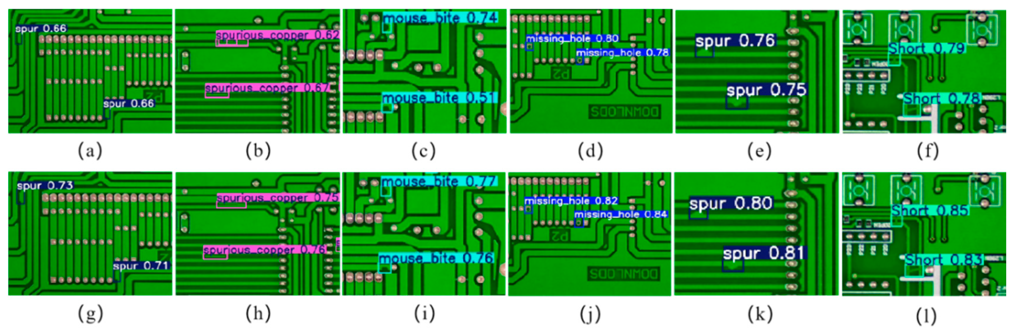
Figure 13 presents a comparison of detection results before and after the improvement of the YOLOv11 model.
Figure 13a–f show the detection results of the original model for six types of defects, while g–l display the results of the improved ESI-YOLOv11n model for the corresponding defects. It can be observed that the overall detection effect of the improved ESI-YOLOv11n model is more outstanding. Regarding confidence scores, ESI-YOLOv11n generally exhibits higher scores, achieving overall superiority over the original model. In terms of detection accuracy, the ESI-YOLOv11n model provides more precise annotations of defect detection boxes, with a relatively lower missed detection rate and higher annotation consistency, which represents a significant improvement over the performance of the original model.
3.8. Failure Mode Analysis
Despite ESI-YOLOv11n achieving excellent average detection precision and AP metrics across various categories in PCB defect detection tasks, a statistical analysis of error samples in the test set reveals that a small number of false positives (FPs) and false negatives (FNs) still exist.
3.8.1. Typical Failure Modes and Trigger Mechanisms
Based on the test results from the PKU-Market-PCB dataset, three representative failure modes were identified through classified statistical analysis of detection errors. Their specific manifestations and trigger mechanisms are as follows:
False positives caused by substrate texture clutter: A portion of the false positives originates from substrate texture clutter that is statistically similar to defect features. Due to slight process fluctuations in different batches of PCB substrates in the dataset, irregular texture structures form on some substrate surfaces. The local morphology of these structures bears high similarity to the features of copper trace short-circuit defects. During the feature fusion stage, the channel grouping strategy of the EMA mechanism fails to completely separate the semantic features of the two types of structures, leading to the misclassification of such texture clutter as real defects, thus increasing the false positive rate.
False positives induced by label noise: To improve generalization ability, random Gaussian blur, salt-and-pepper noise, and other noise types were introduced during the dataset preprocessing stage. When the model learns features based on samples with such noisy annotations during training, it may misjudge background information in label-offset areas as defect features. Consequently, this leads to false positives in similar background areas during the testing phase. Although this introduces some false positives, as the model’s learning capability deepens, it also enhances its robustness, enabling it to reduce noise-induced false positives compared with the baseline model.
Missed detection of shallow scratches with blurred boundaries: Shallow scratch defects with blurred boundaries account for 15% of the missed detection samples. The depth of such defects is less than 5 um, and the brightness contrast with the substrate surface is less than 10%, which is far below the model’s contrast threshold required by the model for effective feature extraction. The gradient information of the defect boundary is smoothed by background noise, making it difficult for the Spatial Reconstruction Unit (SRU) of the ScConv module to capture clear defect contour features. The insufficient discrimination between the defect area and the background in the feature map, ultimately results in the model failing to detect such weak-signal defects.
3.8.2. Physics Analysis
From the core dimensions of physical informatics, the essence of the aforementioned failure modes can be quantitatively explained through three key indicators: Signal-to-Noise Ratio (SNR), spatial frequency components, and lighting contrast.
Lighting Contrast Threshold: Fluctuations in lighting conditions directly affect the contrast between the defect and the substrate. When the brightness contrast between a shallow scratch defect and the substrate is less than 10%, the absolute value of its feature gradient is less than 20 (within the grayscale range of 0–255). This is below the gradient response threshold of the ScConv module’s spatial reconstruction unit, thus preventing the defect features from being effectively activated. Conversely, false positives induced by label noise essentially occur because the deviation between the true defect feature distribution and the label distribution is larger than 15%. This causes the feature distribution learned by the model to include invalid background frequency components, further leading to misjudgments of background areas with similar contrast during the testing phase.
Feature Submersion Caused by SNR Constraints: The SNR difference between substrate texture clutter and copper trace defects is less than 3 dB. The insufficient discrimination between the two at the feature energy level prevents the EMA mechanism from effectively focusing on real defect features, thereby triggering false positives.
Overlap and Attenuation of Spatial Frequency Components: The spatial frequency spectra of substrate texture clutter and copper trace defects have a high degree of overlap, which compresses the feature differences between the two in the frequency domain. This makes it difficult for the model to achieve effective distinction from the frequency dimension. For shallow scratch defects with blurred boundaries, their high-frequency edge components suffer severe attenuation, leaving only gradual gray-level changes with low spatial frequency. This further narrows the frequency difference from the background, ultimately causing missed detections.
Based on the above analysis, the core reasons for false positives and missed detections of the proposed model in PCB defect detection have been clarified. The optimization strategies implemented during the experimental process also achieved error suppression through adaptive parameter adjustment and training strategy optimization, thus enhancing the credibility and depth of this study.
3.9. Industrial Application of the Method
Leveraging its technical characteristics of “high precision, lightweight design, and strong robustness,” ESI-YOLOv11n can deeply adapt to the practical needs of industrial PCB detection. Its core application scenarios and practical values are as follows:
Online Real-time Detection in PCB Production Processes: Deploying the model in embedded visual inspection systems on the production line enables automated online detection for core processes such as etching, drilling, and soldering. With an average precision of 95.9%, a recall rate of 93.3%, and high inference speed, it satisfies the real-time requirements of industrial production lines. This solution can replace traditional manual visual inspection, reducing labor costs for quality inspection by more than 80%. Simultaneously, it controls the defect leakage rate within a low range, effectively avoiding batch rework losses caused by defects flowing into downstream processes.
Low-cost Embedded Hardware Deployment: With a lightweight size of 13.3 MB, the model can be deployed on low-cost edge computing devices such as the NVIDIA Jetson Nano and Huawei Atlas 200I. The hardware investment cost for a single detection unit is only 1/3 to 1/2 of that of traditional machine vision systems. Furthermore, it supports offline inference modes, which is suitable for the intelligent upgrade needs of old production lines in small and medium-sized enterprises.
Data-driven Quality Control Upgrade: The model can be linked with the Manufacturing Execution System (MES) on the production line to record information on the time, location, and type of defect occurrences. This generates defect distribution heat maps and process correlation analysis reports, providing reliable data support for production equipment fault localization and process parameter optimization. This assists enterprises in transforming their quality control mode from “passive detection” to “active prevention.”
Stable Detection in Complex Industrial Environments: In typical industrial interference scenarios such as fluctuations in lighting intensity and dust coverage on board surfaces, the model exhibits minimal attenuation in detection precision, outperforming mainstream detection models. This satisfies the environmental adaptation requirements for PCB defect detection in the industrial manufacturing field.
4. Experimental Conclusions
To address the issues of accuracy bottlenecks, weak generalization ability, and low robustness faced by current PCB surface defect detection methods, this study proposes an optimized algorithm for printed circuit board (PCB) defect detection based on the YOLOv11 architecture—ESI-YOLOv11n. Experiments were conducted and validated on the public PKU-Market-PCB dataset, which contains typical samples of 6 PCB defect categories and can effectively verify the practical detection performance of the algorithm. Additionally, image enhancement techniques were employed to improve the quality of the dataset, thereby strengthening model robustness. To further boost model performance, first, this paper adopts ScConv to refine the C3k2 module, forming a new dynamic and adaptive feature extraction unit that significantly enhances the capability of extracting small-target defect features. Second, a novel EMA mechanism is introduced and embedded into the Neck layer to make the training process more focused on generalization and stability, enhancing multi-scale feature extraction and fusion capabilities, thereby achieving breakthrough improvements in robustness, noise-resistance performance, and overall PCB defect detection performance. Finally, the Inner-IoU concept is integrated into the CIoU loss function to construct Inner-CIoU, which dynamically expands the regression range through parameter-controlled auxiliary boxes and enhanced geometric constraints. The proposed model exhibits significant advantages over other models in terms of accuracy, recall and robustness, and better meets the practical requirements of the PCB defect detection field.
Although the model proposed in this paper has achieved satisfactory results in PCB defect detection, it still has certain limitations. Although the combined design of ScConv and EMA mechanism has improved model performance, it has not achieved deep lightweight fusion of their computational logics, resulting in a model inference speed slightly lower than that of the baseline YOLOv11n architecture, and there is still room for optimization in real-time detection scenarios for ultra-high-speed industrial production lines. The application of the ESI-YOLOv11n model to real-world industrial PCB detection scenarios also faces practical challenges. Industrial production lines impose strict requirements on the real-time performance of detection systems, and the detection equipment used by some small and medium-sized enterprises mainly consists of low-computing-power embedded hardware. The slight increase in model computational cost may become a constraint for online deployment on ultra-high-speed production lines. How to further achieve model lightweighting while ensuring detection performance is the core challenge for its practical industrial deployment. Nevertheless, even though the computational load is slightly higher than that of baseline models, the 13.3 Mb model size is still suitable for current industrial mobile deployment. In future work, our team will focus on research into model lightweighting, while further enhancing the stability and detection efficiency of the model.