Article

Real-Time Temperature Estimation of the Machine Drive SiC Modules Consisting of Parallel Chips per Switch for Reliability Modelling and Lifetime Prediction
School of Engineering, Computing and Mathematics, The University of Plymouth, Plymouth PL4 8AA, UK
*
Author to whom correspondence should be addressed.
Machines 2025, 13(8), 689; https://doi.org/10.3390/machines13080689
Submission received: 13 June 2025 / Revised: 22 July 2025 / Accepted: 28 July 2025 / Published: 5 August 2025
(This article belongs to the Special Issue Power Converters: Topology, Control, Reliability, and Applications)

Abstract

This paper presents a new methodical procedure to monitor in real time the junction temperature of SiC Power MOSFET modules of parallel-connected chips utilized in machine drive systems to develop their reliability modelling and predict their lifetime. The paper implements the on-line measurements of temperature-sensitive electrical parameters (TSEP) approach, particularly the quasi-threshold voltage and the on-state drain to source voltage, to estimate the junction temperature in real time. The proposed procedure firstly applied computational fluid dynamics analysis on the module under study to determine the chip which undergoes the maximum junction temperature during typical operation of the module. Then, a calibration phase, using double-pulse tests on the selected chip, is used to generate look-up tables to relate the TSEPs under study to the junction temperature. Next, the real-time estimation of junction temperature was accomplished during the on-line operation of the three-phase inverter, taking into account the induced distortion/noises due to operation of the parallel-connected chips in the module. After that, a comparison between the two TSEPs under study was provided to demonstrate their advantages/drawbacks. Finally, reliability modelling was developed to predict the lifetime of the studied module based on the estimated junction temperature under a predetermined mission profile.

1. Introduction

Recent technological advances in power semiconductors have made wide bandgap (WBG) power semiconductor devices, such as Silicon Carbide (SiC) or Gallium Nitride (GaN), an attractive substitute for their silicon counterparts, thanks to their potential higher power density, higher blocking voltage and less switching losses [1,2]. Moreover, the reliability of such devices becomes of paramount importance especially in critical applications such as aerospace and military fields. It is also well known that operating conditions significantly affect the reliability of these power electronic components. The most significant stress factors of power electronic modules are temperature and temperature cycling which result in thermo-mechanical stress due different coefficients of thermal expansions (CTEs) of materials in the modules [3,4]. Repetitive thermal cycling can eventually cause cracks, solder voids and delamination within module interconnection resulting in increased thermal resistance and ultimately even higher junction temperatures (Tj) [5]. Consequently, on-line estimation of junction temperature during the operation of a power electronic converter is therefore essential for its condition monitoring, which can potentially improve its reliability by providing real time up-to-date information for the devices’ health states, and ultimately predicting the remaining useful lifetime [6,7,8].
Real-time measurements of junction temperature (Tj) can be accomplished using one of three approaches [9,10]: optical approach, physical contact approach, or temperature-sensitive electrical parameters (TSEP) approach. Table 1 summarizes the number of applications for each of these approaches. It shows that the TSEP approach has the superiority over the other approaches since it provides on-line monitoring for Tj of the device without the need to modify its module. Furthermore, from the stated literature in Table 1, it demonstrates the advantageous Vth and VDSon methods to capture the Tj due to their better sensitivity and higher resilience to the electromagnetic interference (EMI) over a wide operating range comparing to other TSEP methods.
Furthermore, some other recent papers have also investigated the application of TSEP methodologies in WBG power devices such as SiC power MOSFETs. Table 2 highlights some of their features and drawbacks. On the other hand, the on-line estimation of junction temperature during the operation of parallel-connected chips in SiC MOSFETs modules using the TSEP techniques has not been demonstrated yet in the literature.
Recently, large SiC power MOSFET modules that are utilized in different machine drive applications are typically constructed by paralleling a number of dies in order to increase their output current capabilities. The operation of parallel-connected SiC power MOSFETs has been studied in previous papers, in which important issues such as the distribution of the power losses within the parallel devices, the induced resonances and the parasitic oscillations during their commutation, crosstalk and EMI are investigated and studied. Paper [30] presents the key parameters that play important roles in the performance of the parallel operation of the SiC MOSFETs with respect to the device characteristics as well as the circuit layout. In [31], the impact of the electrothermal variation between parallel-connected devices on overall avalanche ruggedness are analyzed. In addition, experimental losses analysis for two parallel-connected SiC MOSFETs is investigated through a double-pulse test in [32] as well as during the operation of DC/DC boost converter in [33].
Furthermore, even though SiC MOSFET have thermally oxidized insulating SiO2 layers, which have superior dielectric properties, the Vth of such devices suffers from instabilities due to their bias temperature stress (BTS) behaviour. Their BTS causes trapping of carriers near the SiC/SiO2 interface, which produces a variation in output characteristics of the devices. The presence of carbon atoms during the thermal oxidation of SiC causes a SiC/SiO2 interface with higher magnitudes across the interface to trap density and oxide charges compared with the traditional Si/SiO2 interface [34]. Additionally, the SiC/SiO2 interface is also different from the Si/SiO2 interface due to its narrower band offsets which reduces the barrier for carriers to scale that leads to the gate leakage current and the gate dielectric degradation. Due to this threshold voltage shift, the positive and negative bias temperature instability contributes to inhomogeneous current distributions in the system, which eventually degrades the commutation of the device and increases its temperature [35,36,37].
Despite of all these challenges in estimating the Tj of SiC MOSFETs devices by TSEP approach, especially in parallel-connected arrangements, this presented paper has achieved the real-time estimation of the Tj of such devices with high accuracy and minimum error with respect to the actual temperature measurements.
This paper presents a systematic route for real-time estimation for the Tj of SiC power MOSFETs modules consisting of paralleled chips per switch using the on-line measurements of Vth and VDSon. VDSon and Vth have been selected for estimating the Tj in this paper since they present better temperature sensitivities and higher noise immunities compared to other TSEPs utilized in Tj estimation of semiconductor devices, such as internal gate resistance, saturation current and the switching on/off times.
A measuring board has been designed in this research to cope with the operation of the modules of paralleled connected chips and capture the TSEP under study in a non-invasive manner during real-time inverter operation. The proposed TSEP monitoring is evaluated in a SiC MOSFET prototype module consisting of six paralleled chips per switch. In order to identify the chip to which the TSEP-based monitoring is applied, a computational fluid dynamics (CFD) analysis has been performed in Section 3 to determine the hottest chip during a typical operation. A calibration procedure, using double-pulse tests, is then used in Section 4 to construct look-up tables relating the proposed TSEPs with the Tj of the SiC MOSFET module under the study. In addition, the captured measurements of Vth during the double-pulse tests have gone through distribution and curve-fitting techniques in order to overcome the challenges associated with the Vth divergences in SiC MOSFETs devices due to the induced distortion/noise during the operation of paralleled chips. Subsequently, the real-time estimation of Tj has been implemented in Section 5 and validated for a SiC MOSFET-based three-phase power inverter. Moreover, the two proposed TSEPs under study are compared based on the outcomes of the real-time operation according to their performance and feasibility for modules of parallel-connected chips. Eventually, reliability modelling was then developed in Section 6 for the studied module based on the estimated Tj to predict its lifetime within a predefined mission profile. The lifetime prediction has been performed through Rainflow algorithm and histogram analysis along with the Coffin–Manson model based on the power cycling tests which have been undertaken by the module manufacture. At last, Section 7 discusses the influence of the ageing effects of the SiC power module on the studied TSEPs as well as a refinement process is proposed to amend the Tj estimation to include the deviations in the measured TSEP due to the degradation effects of the module.

2. Proposed Methodical Procedure for the Tj Estimation

A measuring board has been developed in this research for on-line capturing of the VDSon and Vth for the modules of multiple chips per switch. The developed board emphasizes the non-invasive monitoring of the TSEPs under study during the real-time operation of the three-phase inverter, taking into consideration the induced noises due to the operation of module, which consists of parallel chips per switch.
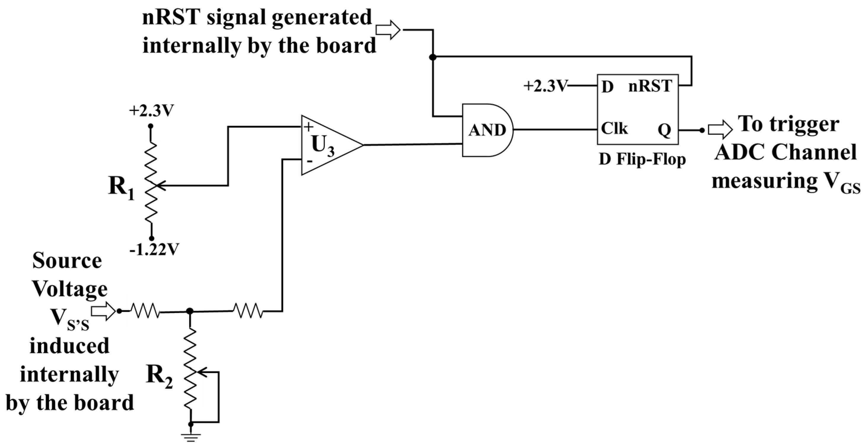
Schematic circuits for capturing the VDSon and Vth are demonstrated in Figure 1 and Figure 2, respectively. The VDSon is acquired during the on-state period. The switch Q1 in Figure 1 is used to disconnect the low voltage measuring circuit from the high voltage drain of the power MOSFET during turn-off. A signal conditioning circuit is also utilized to scale the measured signal to a suitable range for the measuring ADC channels. Figure 2 illustrates the schematic of the triggering circuit that is employed to trigger the ADC channel measuring the gate-to-source voltage (VGS). The main challenge in on-line measurement of Vth lies in the capturing of the gate voltage at the correct instant at the start of the device conduction time. In this paper, the voltage across the parasitic inductance between the auxiliary Kelvin source (S’) and the source (S) is employed to capture the required Vth signal [38]. This voltage (VS’S) is generated when the device current IDS starts to rise during device turn-on. The rising edge of the VS’S across the parasitic inductance can be then used to trigger the ADC channel measuring the gate–source VGS effectively at the start of conduction and therefore acquire the Vth measurement. Accordingly, the measurement of the drain-to-source current IDS is not needed to detect the Vth value in this approach.
Moreover, ferrite beads have been included after each voltage regulator in the measuring board to reduce the oscillations in the generated voltage levels due to the parasitic oscillations between the connected chips [39], and an additional opto-isolation circuit has been implemented between the control and the gate drive circuits to minimize the ground loop in the system [40].
Accordingly, the flow chart of the proposed methodical procedure in this paper for estimating the Tj of the parallel-connected SiC power modules in real time is demonstrated in Figure 3 to be utilized, ultimately, to develop their reliability modelling and predict their lifetime.

3. Thermal Analysis for the SiC MOSFET Module

The power module used in this work, Figure 4, is a SiC MOSFET-based half-bridge. The module has been designed and manufactured by Siemens AG, to provide a power electronic building block (PEBB) for a 99% efficient three-phase power converter with a power-to-weight ratio of 10 kW/kg. Figure 5 shows the CAD drawings of the half-bridge wire-bond-less power module. Twelve MOSFETs were sintered using a silver sintering paste onto the direct copper bonded (DBC) substrate. Since each switch is obtained by parallel connection of six MOSFET dies, in order to identify the device to be monitored in the final application, a computational fluid dynamics (CFD) simulation analysis has been carried out for the module under the study to identify the device with the highest Tj.
The simulation has been established in the ANSYS 2021 R2 Icepak CFD tool to solve the conjugate heat transfer (CHT) phenomena between the different components in the module and the surroundings. The configurations of the utilized CFD simulation are as follows:
  • The inlet air temperature is at 40 °C with a fixed airflow rate of 4 m/s.
  • SiC chips with thermal conductivity of 150 W/mK.
  • Since the thermal conductivity of SiC is temperature dependent and decreases with temperature, the worst-case value for conductivity has been chosen in this paper at Tj = 125 °C [41,42].
  • Silver sintering simulated as a solid with thermal conductivity of 250 W/mK [43] and thickness of 100 µm.
  • DBC copper Si3N4 layers with thermal conductivities 398 and 85 W/mK.
The thermal analysis shown in Figure 6 demonstrates that chip number 9 suffers from the highest Tj in steady-state conditions with total power losses of 150 W, equivalent to 12.5 W per chip. Therefore, this chip will be chosen for the TSEP monitoring in this paper by capturing its VDSon and Vth to be utilized for the proposed estimation of the Tj in the paper.

4. Double-Pulse Tests

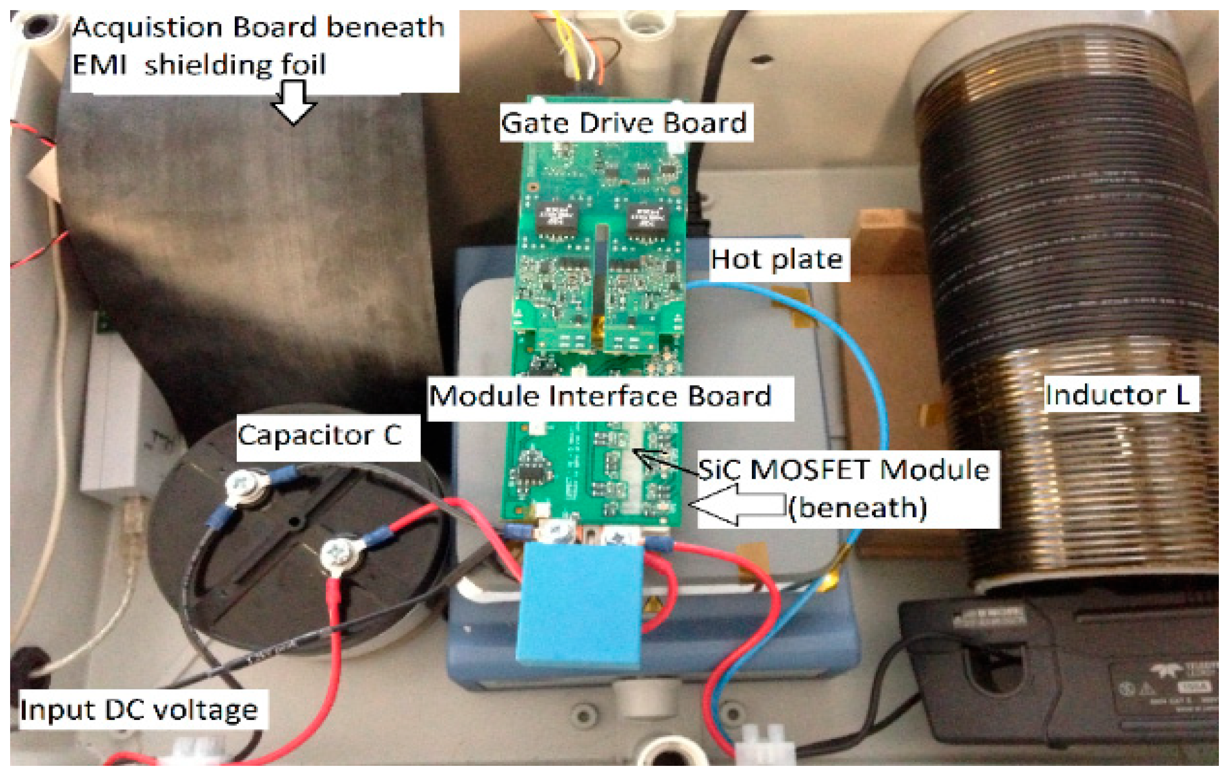
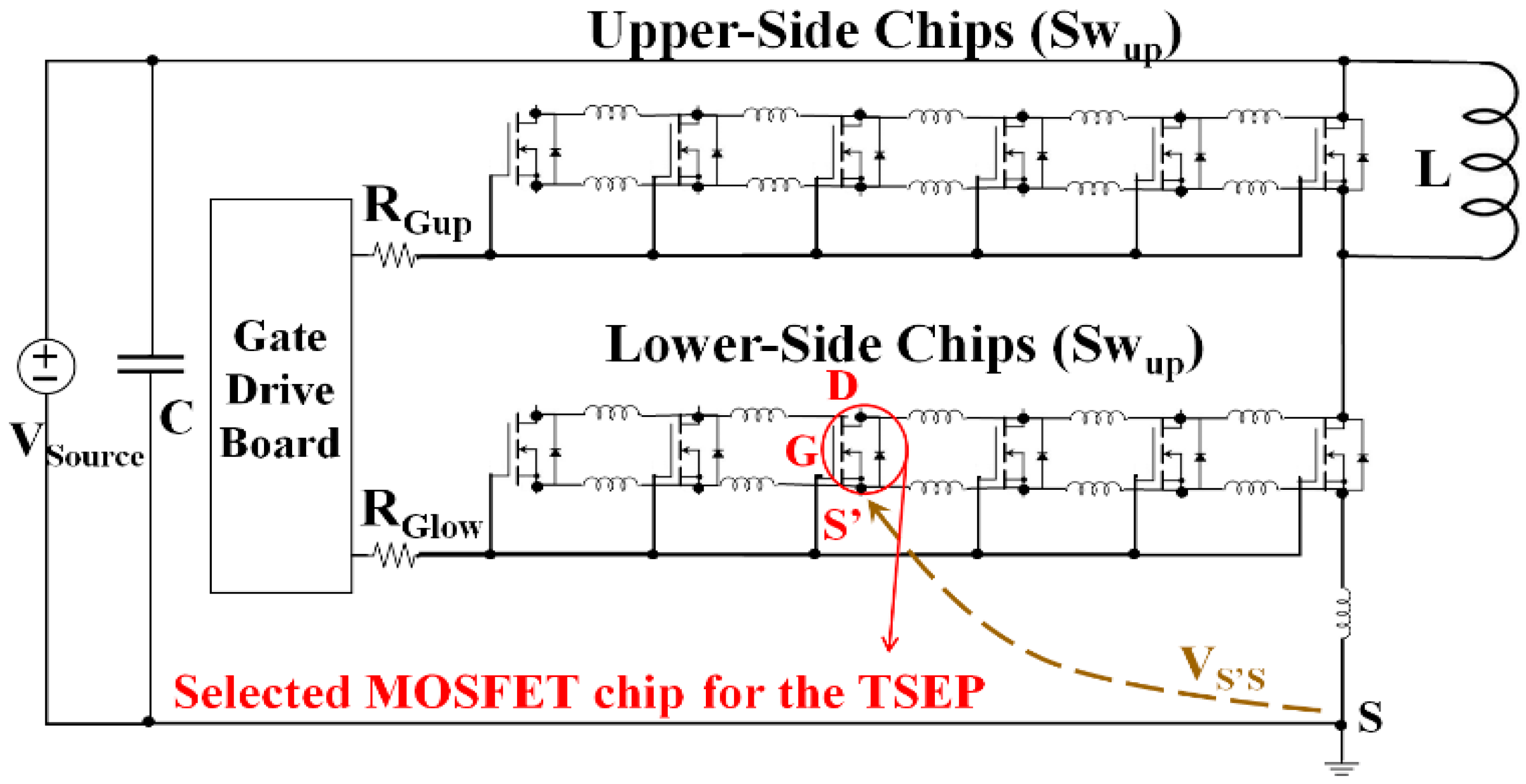
Double-pulse tests have been performed on the SiC Power MOSFET module under study for the purpose of directly correlating the measured TSEPs with a known device temperature and therefore provide calibration look-up tables to be used in real-time implementation. The experimental setup utilized in the double-pulse test is shown in Figure 7 along with its schematic circuit in Figure 8 in which the nominated MOSFET chip implemented in the TSPE under study is indicated with its VS’S measurement.
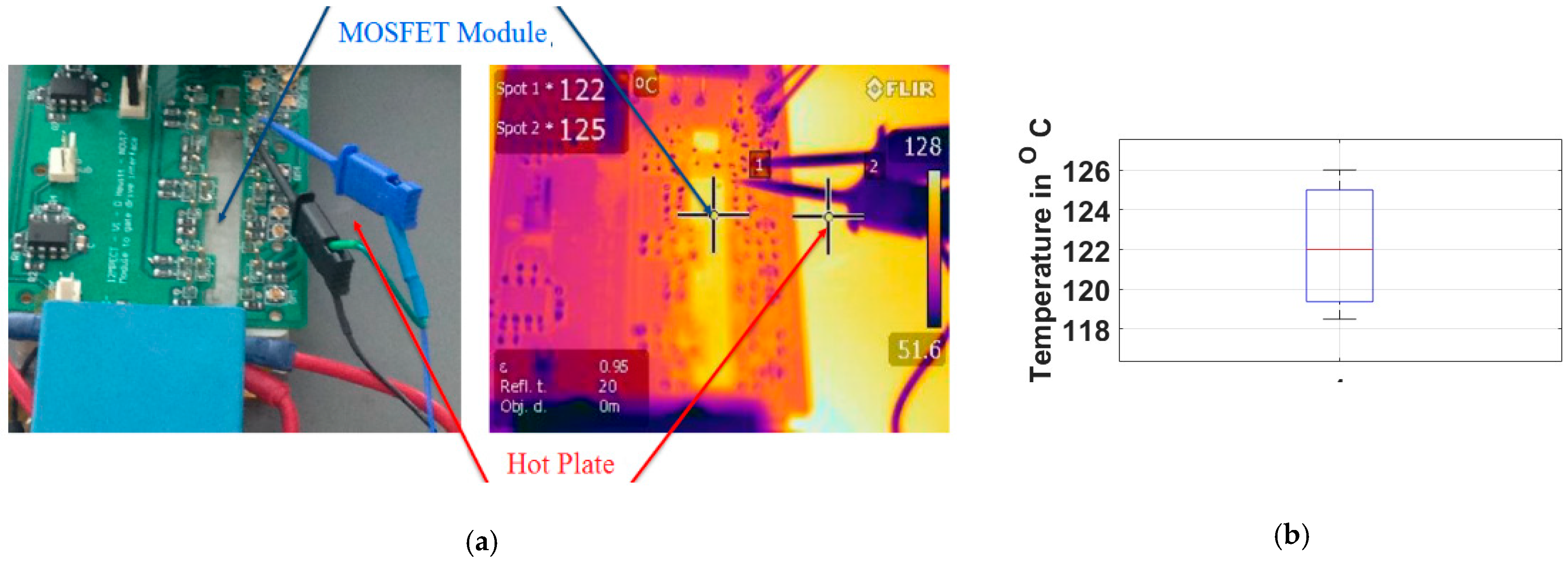
A hot plate, as shown in the experimental setup, is used to accurately control the junction temperature of the MOSFET module during the tests. Direct measurement of the junction temperature is performed using a thermal camera capturing the die temperature of the module. The module upper surface is accessible in the given experimental setup through a gap in the gate drive interface board as shown in Figure 7. In this experimental setup, an air-cored inductor (170 μH) is used as load (L) and film capacitor (C) of 600 uF–900 V and has been inserted across the DC bus. A gate drive board (Prodrive Technologies PT62SCMD12) has been used in these tests.
According to the schematic circuit in Figure 8 the lower side switch (Swlow) is the main switch under study, in which its TSEPs are monitored and captured during the tests using the measuring board. On the other hand, the upper side switch (Swup) will act as a diode by providing negative voltage to its gate. Furthermore, Figure 8 illustrates the voltage VS’S over the parasitic inductance which is used to trigger the ADC channel of the Vth measurement.
Figure 9 and Figure 10 illustrate, at the junction temperature 100 °C and 20 °C, respectively, the VGS measurement and the voltage signal Vtrig1 of the circuit of Figure 2, which is used to trigger the ADC channel of the Vth measurement. As shown in both figures, the main distinction between the two different Tj is in the initiation time of the Vtrig1 with respect to VGS value and its dependence on the Tj. As the Tj increases, the switch will be able to create a conductive channel between drain and source faster than that at lower Tj condition with the same DC bus voltage. This eventually leads to lower Vth voltage value with increasing of the Tj. Accordingly, the Vtrig1 signal is generated sooner in the case of Tj = 100 °C and the corresponding ADC will then initiate conversion earlier, i.e., with VGS =3.45 V as shown in Figure 9, compared to VGS = 3.85 V for the 20 °C case in Figure 10. The captured measurements by the ADC channels are transferred to a graphical user interface (GUI) through a serial peripheral interface (SPI) communication.
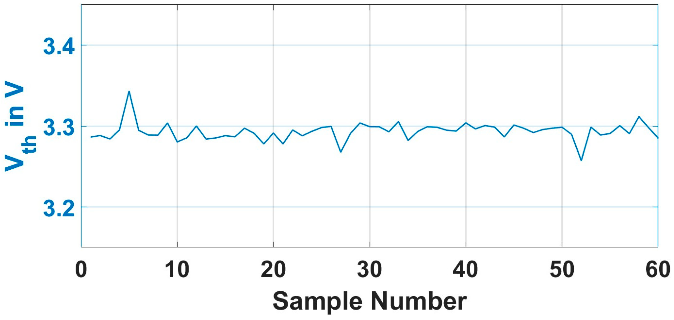
The acquired measurements for Vth at the 100 °C and 20 °C by the ADC channel are illustrated in Figure 11 and Figure 12, respectively. It is worth noting that there is an offset of approximately 0.55 V between the Vth captured by the ADC channels (Figure 11 and Figure 12) and those illustrated by the oscilloscope and the voltage probes (Figure 9 and Figure 10). This is mainly due to the low pass filter effect of the larger input capacitance of the voltage probes on the captured signals, which causes a delay in measuring the signals by the oscilloscope.
It is also worth to mention that the sampling frequency that has been used in the paper for the double-pulse tests (as well as the following real-time operation) is 10 kHz, equivalent to 100 usec sample time, while the required ADC conversion and measuring times during the tests typically take 0.92 usec. Consequently, the ADC process is almost undertaken within 1% of the sample time of the testing operations, so the error due to these ADC processing times is avoided. On the other hand, the total delay time, from applying the triggering signal of VS’S at the input of the trigger circuit (Figure 2) until the ADC unit initiates its conversion process, is taken around 5.3 nsec only so that an accurate measurement of Vth is achieved from the VGS profile during the turning-on of the SiC device given that the rise time of the VGS during the turn-on period is around 200–300 nsec.
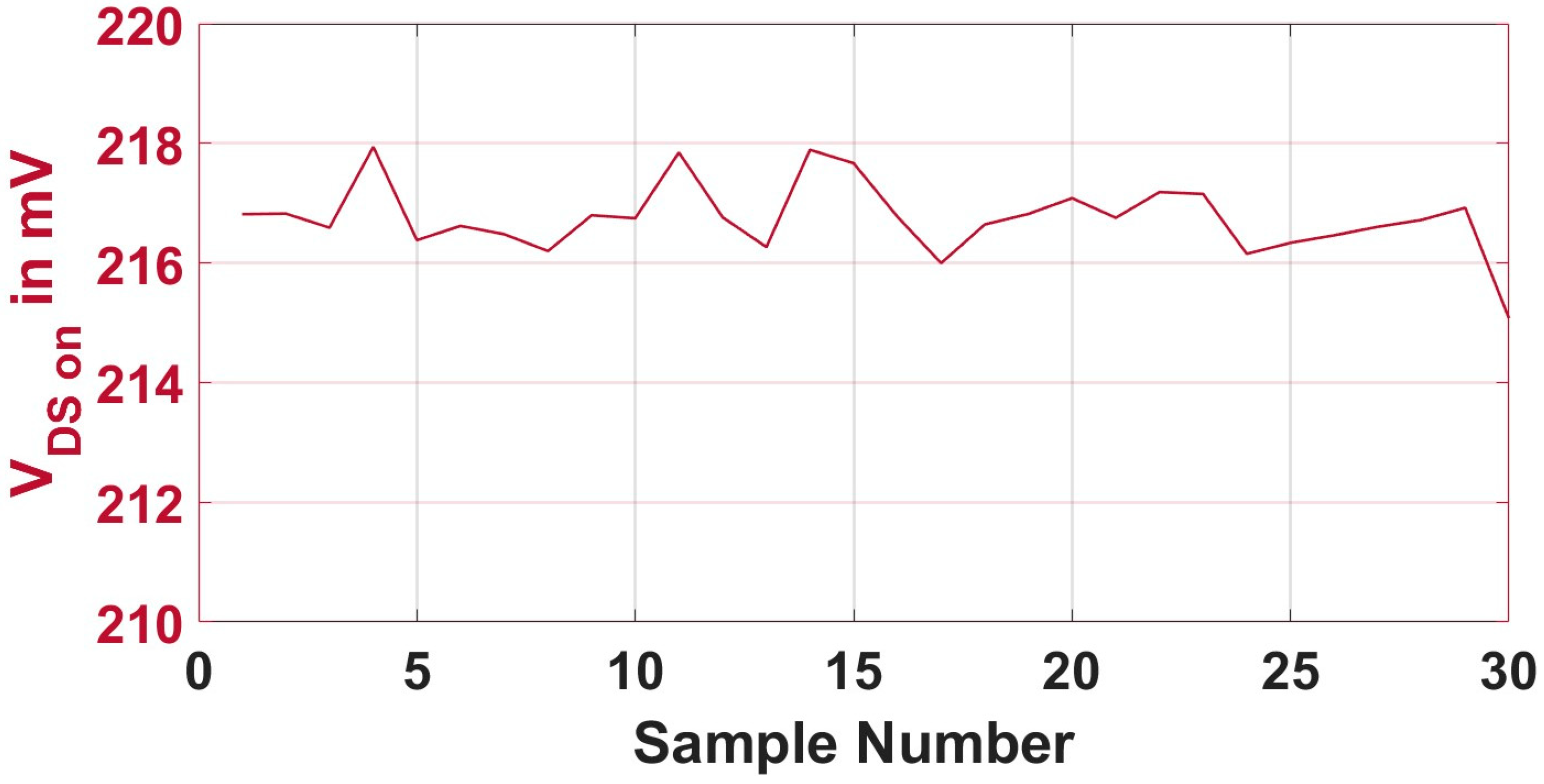
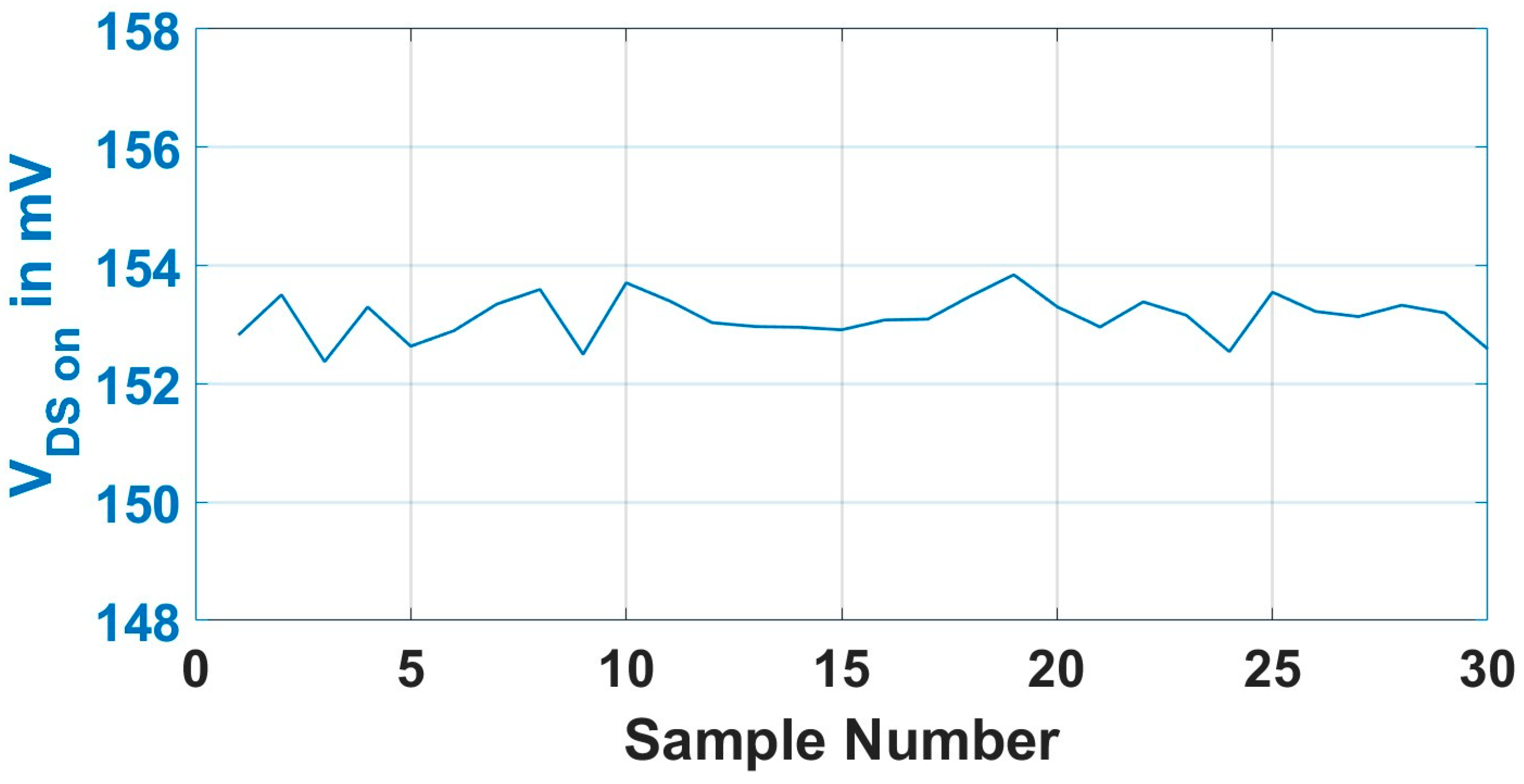
Figure 13 and Figure 14 show the VDSon signals captured by the ADC channel at 100 °C and 20 °C, respectively. Since the on-state resistance (RDSon) has a positive temperature coefficient, i.e., it increases as Tj increases, consequently the VDSon also increases with Tj but with a potentially nonlinear and current-dependent relationship.
Accordingly, based on the captured measurements through Figure 11, Figure 12, Figure 13 and Figure 14, it is demonstrated that the captured TSEP, Vth and VDS-on, are mostly steady and constant across the measuring interval taking into the account the same operation and temperature condition. Figure 11 and Figure 12 illustrated a maximum deviation of 5% had occurred for Vth measurements, while Figure 13 and Figure 14 shows a maximum deviation of 1% had taken place in VDSon measurement.
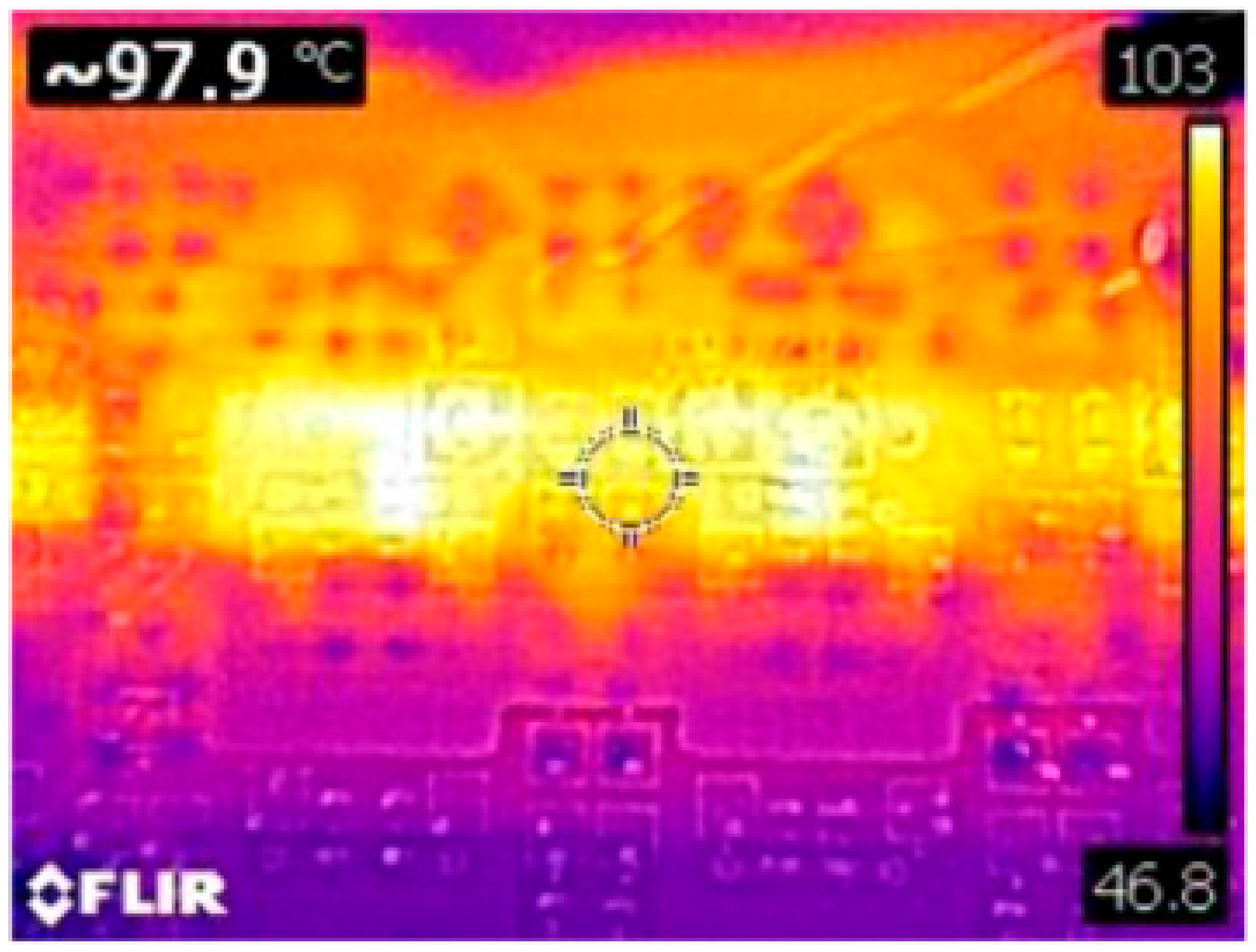
Figure 15 shows that the gate driver adapter board, mounted on the power module, features a cut-out that allows direct visual and physical access to three of the twelve SiC MOSFET dies in the module. The top surface of the module is coated with boron nitride paint to provide a high emissivity surface for the thermal camera. The temperature measurements for the three visible dies are illustrated in Figure 16 which indicates the temperature variations within these three dies to be around 5%. Figure 15 also illustrates the micro-coaxial contact, SM, in the gate driver adaptor board that enables the access to measure the VSS’.
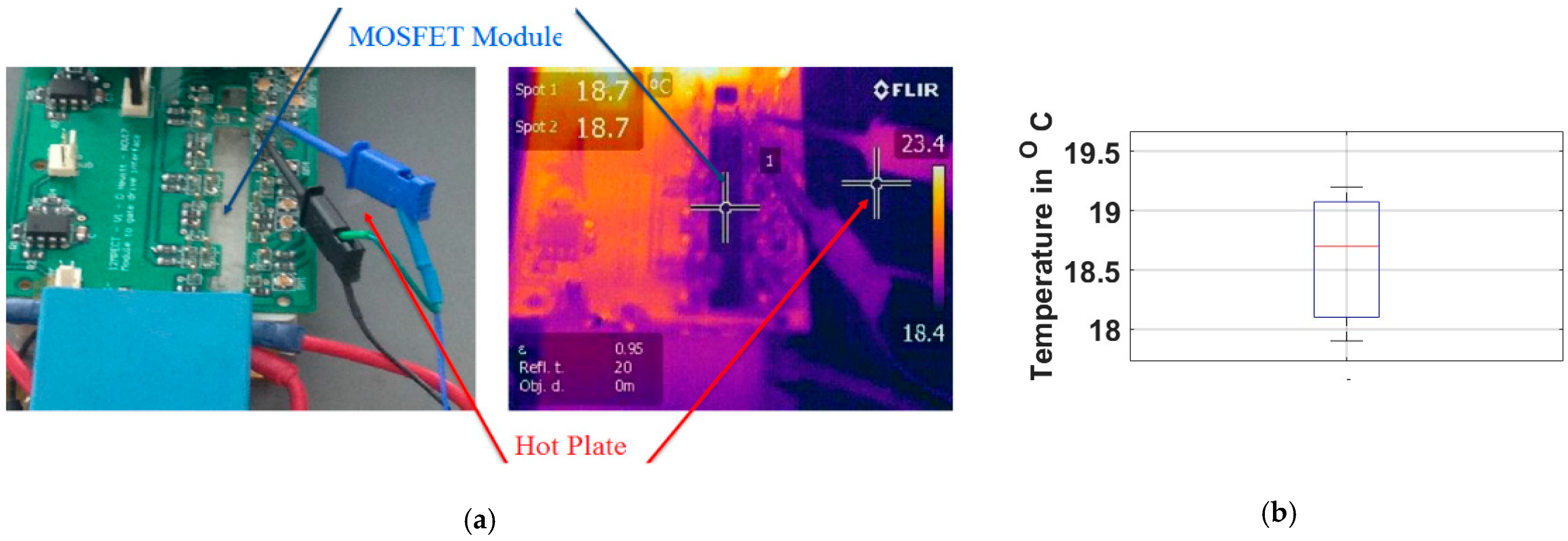
A series of double-pulse tests have been carried out on the SiC Power MOSFET module under the study at 500 V DC throughout different Tj and different drain-to-source currents (IDS). The Tj has been independently measured using a thermal camera as shown in Figure 17 and Figure 18. The thermal imaging is calibrated via the thermal camera software by taking the average temperature across the MOSFET die under study. Examples of thermal measurement error analysis is illustrated in Figure 17 and Figure 18 as well using a boxplot approach.
An example of the waveforms of the VGS, VDS, IDS and the load current (Iout) during one double-pulse test at 19 °C Tj is shown in Figure 19 in which the magnitude of the Iout is controlled by the width of the first pulse of the test. However, the second pulse is used to maintain the current at the required value during acquiring the TSEP by the measuring board. Iout is captured using the LECROY-CP150 current probe; however, IDS is acquired using CWT Ultra-mini Rogowski coil.
In order to disregard the false triggering events in measuring the Vth in the SiC MOSFET devices, a filtering based on a voltage band around the expected values of Vth is applied. In addition to that, the captured values of both Vth and VDSon have also been post-processed to develop the best relationship that correlates the Tj to TSEP under study with the lowest error to overcome the variations in both TSEPs due to the induced distortions during the operation of the paralleled connected chips. Figure 20 and Figure 21 present an example of these applied post-processing analyses in this paper.
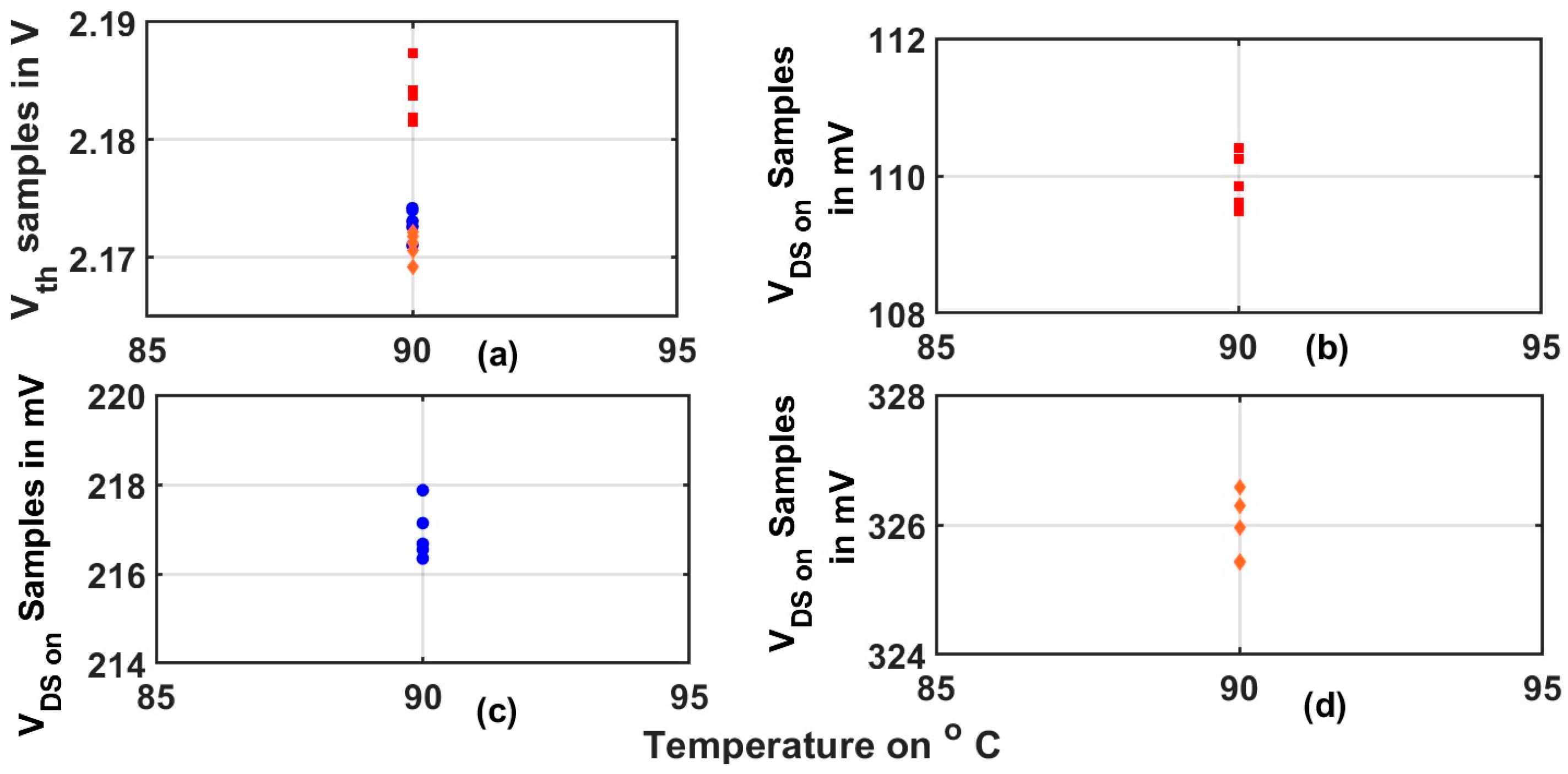
Figure 20a–d show the number of captured samples of the TESPs under study at Tj equals 90 °C with different load currents 20 A, 40 A and 60 A. Figure 21 illustrates the applied distribution fitting approach to process the captured Vth samples of Figure 20a. Firstly, the histogram of the captured samples is developed to designate the best probability distribution function that could fit the captures values.
As shown in Figure 21, the normal distribution function is a better candidate to represent the captured values based on the developed histogram. After that, the mean value of the estimated distribution function is then calculated to represent the value of the Vth at this testing instance. Similar to the VDSon captured samples, but this is repeated at each output current value (IO) as illustrated in Figure 20b–d, since this parameter is current dependant. Accordingly, this distribution-fitting technique has been carried out for all captured samples of the TSEP under study in order to select the proper value that could represent the measured TSEP at each testing condition. It has also been recognized that the variance of the fitted distributions for the captured samples of the two TSEPs are relatively increasing with the increase of Iout as well as Tj since both factors contribute to raising the effect of the induced noise and parasitic oscillations generated during the operation of the parallel chips of the module. Finally, a curve-fitting technique was developed to predict the best relationships with lowest errors between mean values for each TESP and the measured Tj. These relationships are then employed in the upcoming real-time estimation of the Tj in Section 5.
Some of the developed curve-fitting relationships from the applied double-pulse tests are provided in Figure 22 for the VDSon and Figure 23 for the Vth versus different Tj as well as different IO. A good linearity for VDSon with respect to Tj is demonstrated in Figure 22. Sensitives of approximately 1.45 mV/°C and 1 mV/°C are estimated at output currents 60 A and 40 A, respectively. The single-chip datasheet [44] provides a sensitivity of at 5.5 mV/°C at IDS of 50 A, which results in approx. 0.92 mV/°C for six chips per switch, assuming symmetric current sharing between the parallel chips.
The expected negative temperature coefficient of Vth is confirmed along with the invariance to load current as demonstrated in Figure 23. A relatively good linearity is observed. Good sensitivity of around 6.6 mV/°C is comparable to approximately 5 mV/°C given in the device datasheet. The main reasons for this discrepancy are the approach to capture the Vth in the datasheet compared to the method implemented here in this paper.

5. Real-Time Inverter Operation

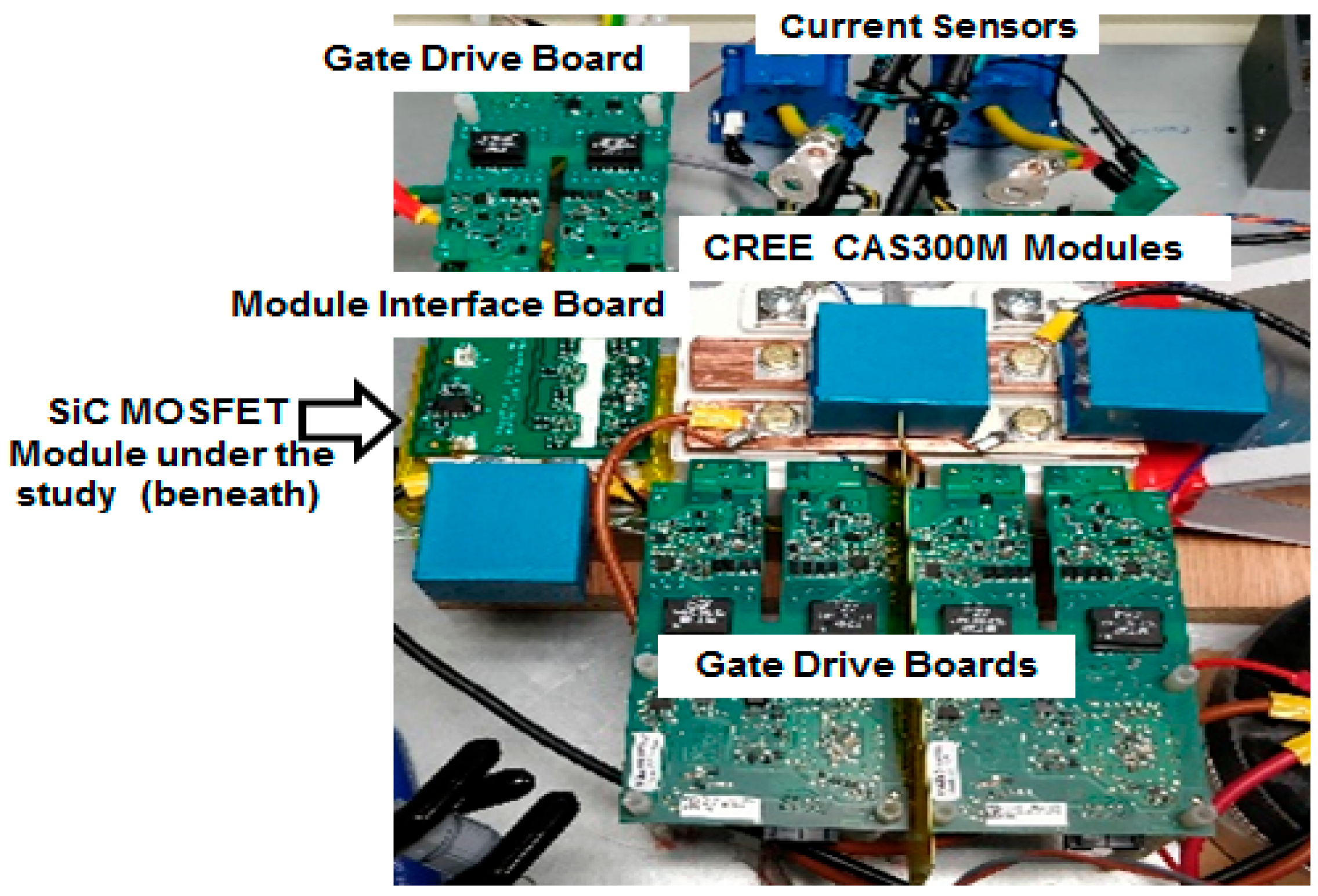
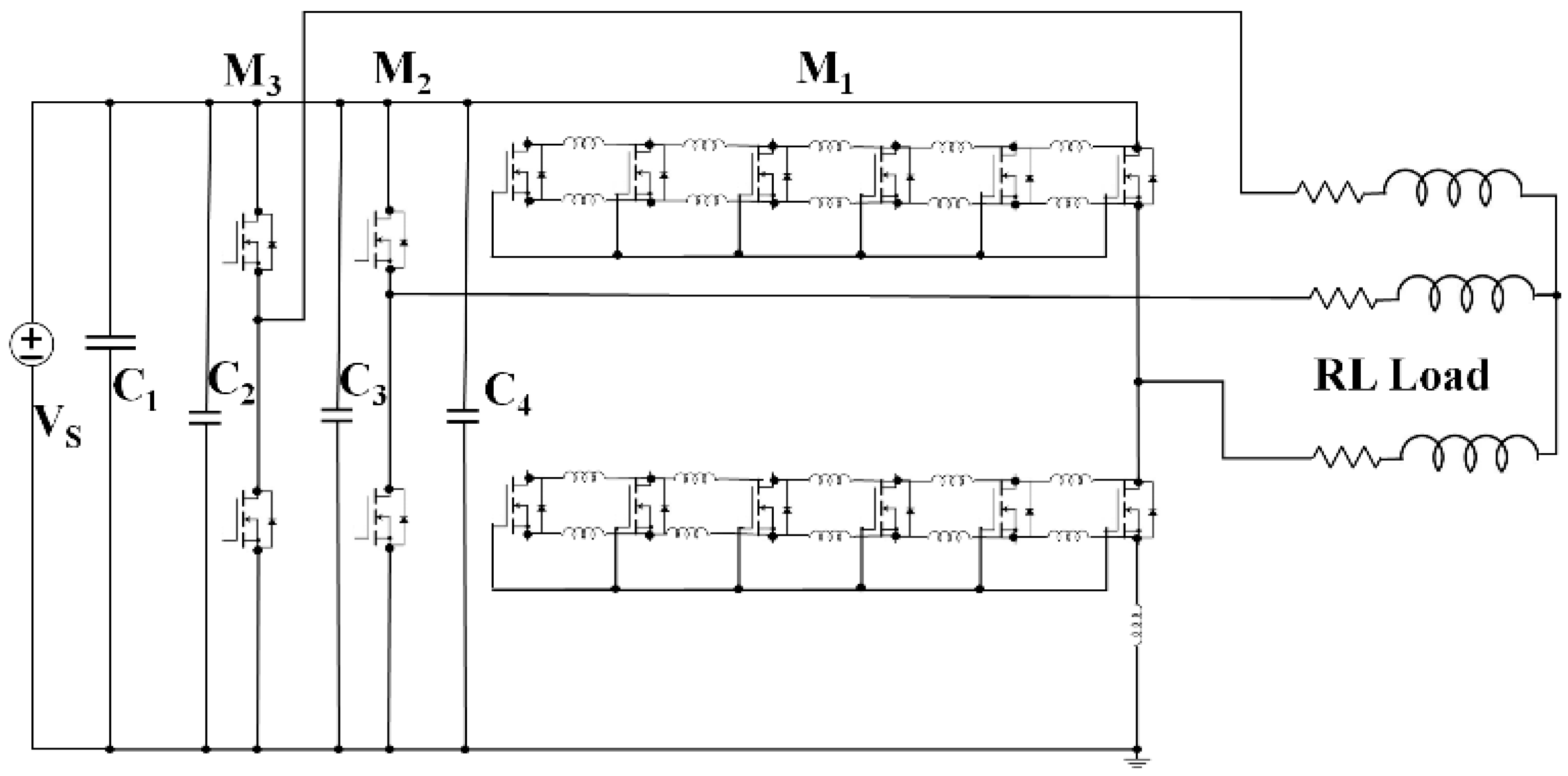
The proposed on-line estimation for junction temperature for SiC MOSFET under the study is evaluated in the real-time operation of a three-phase inverter. The three-phase inverter used for this study is a three-leg half-bridge-based converter used to supply a three-phase RL load. The layout of the three-phase inverter is provided in Figure 24 along with its schematic circuit in Figure 25. Due to the availability of prototype module under the study, the inverter was constructed using only a single prototype module (M1) and the remaining two legs of the converter were implemented using commercial off-the-shelf modules (CREE CAS300M) (M2 and M3). A table of components utilized in this inverter circuit are listed in Table 3 with their descriptions and values. During testing, the inverter was driven so as to output a sinusoidal output current at a frequency of 200 Hz into the load with a 10 kHz switching frequency. To validate the temperature values predicted by the TSEP, a thermal camera has been utilized to measure the die temperature of the module during the inverter operation.

5.1. On-Line Tj Estimation Based on the Vth Measurements

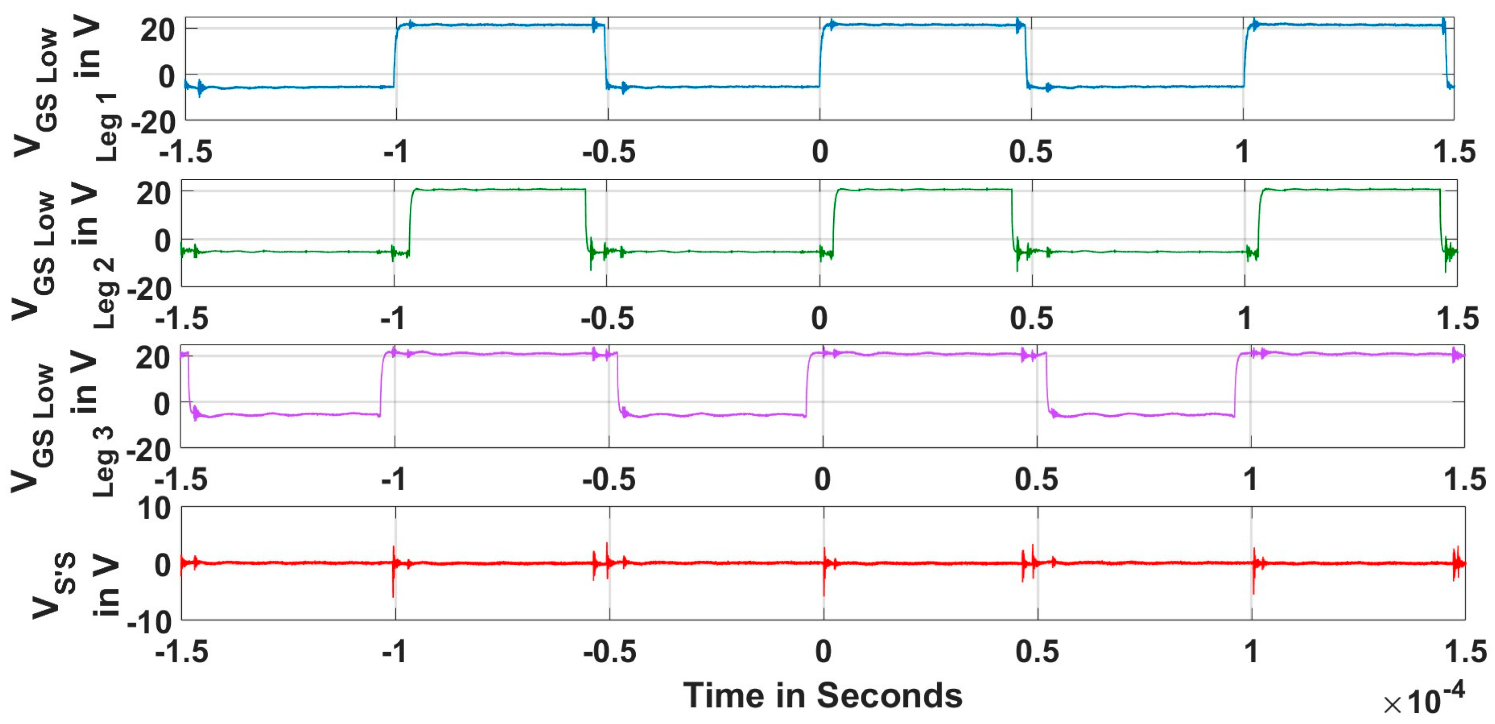
Figure 26 illustrates the waveforms of the gate-to-source voltages (VGS) of the three switches in the lower sides of the three MOSFET modules (legs) in the three-phase inverter. The voltage across the parasitic inductance (VS’S), which is used to trigger the ADC channel to capture the Vth as discussed in previous sections, is shown in the bottom trace in Figure 26.
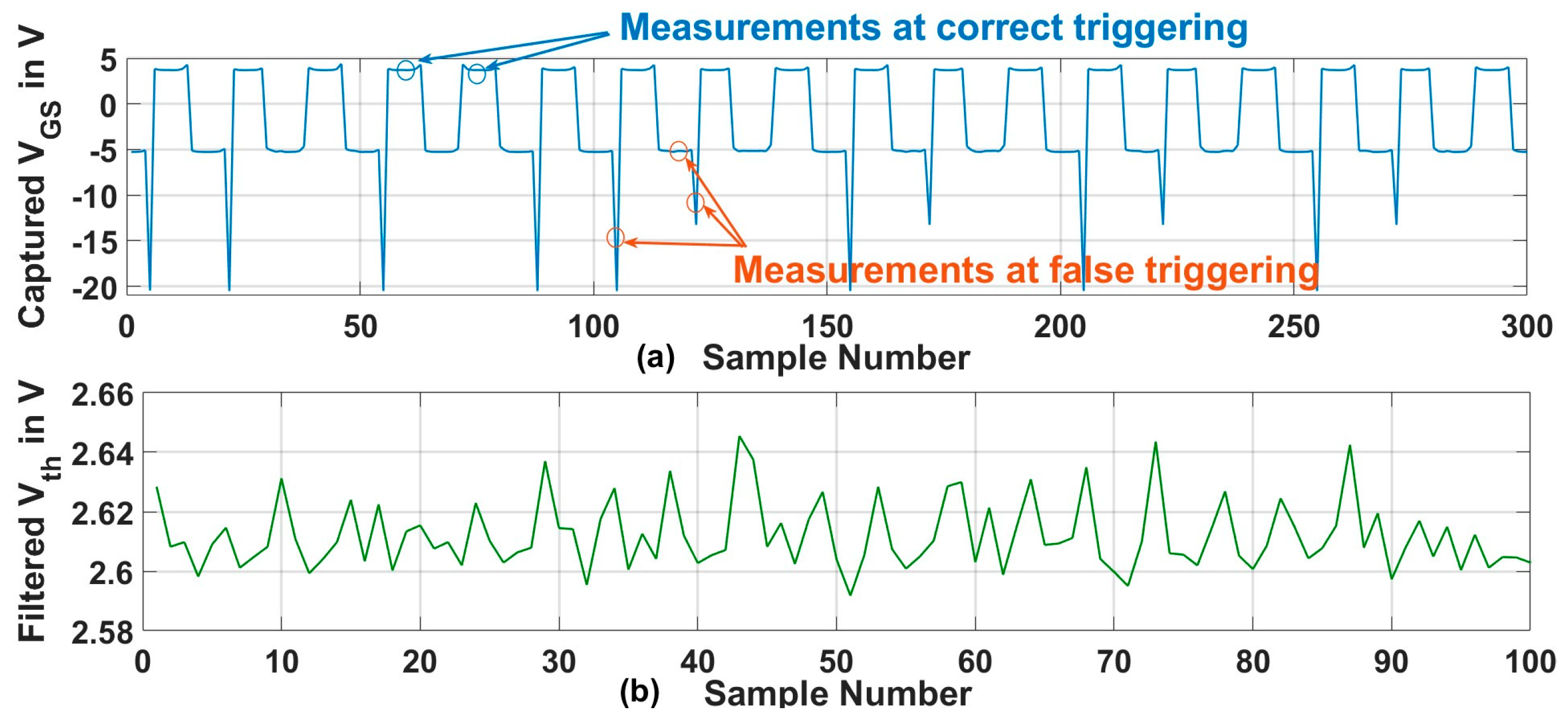
Figure 27a illustrates the signal captured directly by the ADC channel for the Vth measurement. This signal does not present the actual value for the Vth since there is a signal conditioning circuit between the measured point on the VGS and the ADC channel in the measuring board in order to adjust the measured signal to be within the measuring scale of the ADC channel. After suitable scaling, the actual measured Vth is shown in Figure 27b. It is worth noting that during the on-line acquisition of the Vth measurement, false triggering instances for the ADC channel took place, as illustrated in Figure 27a. The main causes of these events are the switching events of other device/chips in the module and the other phases, EMI noise within the system and parasitic module. As shown in Figure 27a, these false triggering events will result in measurements of Vth outside of the typical range and therefore can be discarded from further processing using a filtering based on a voltage band around the expected values of Vth.
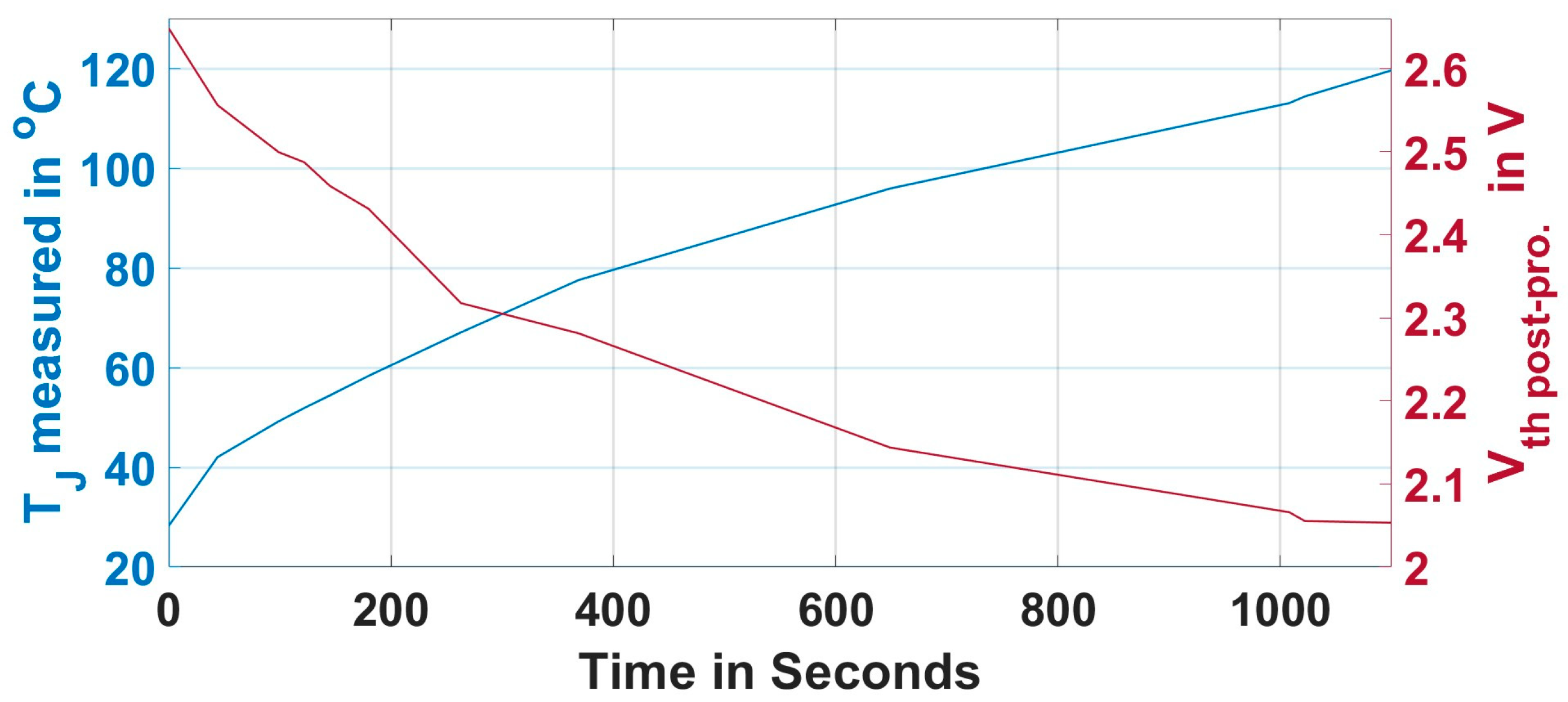
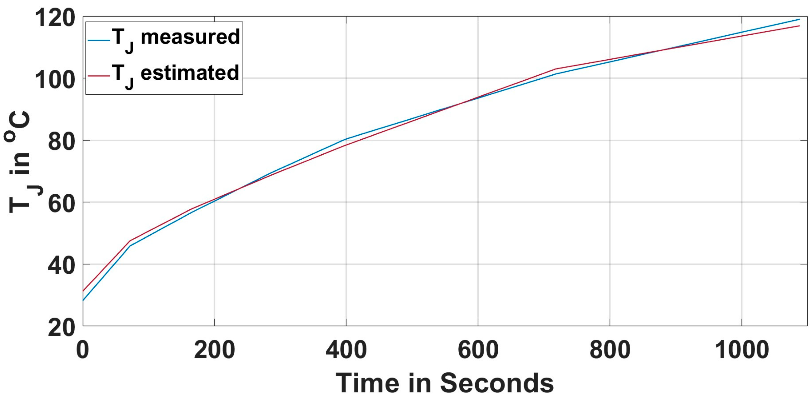
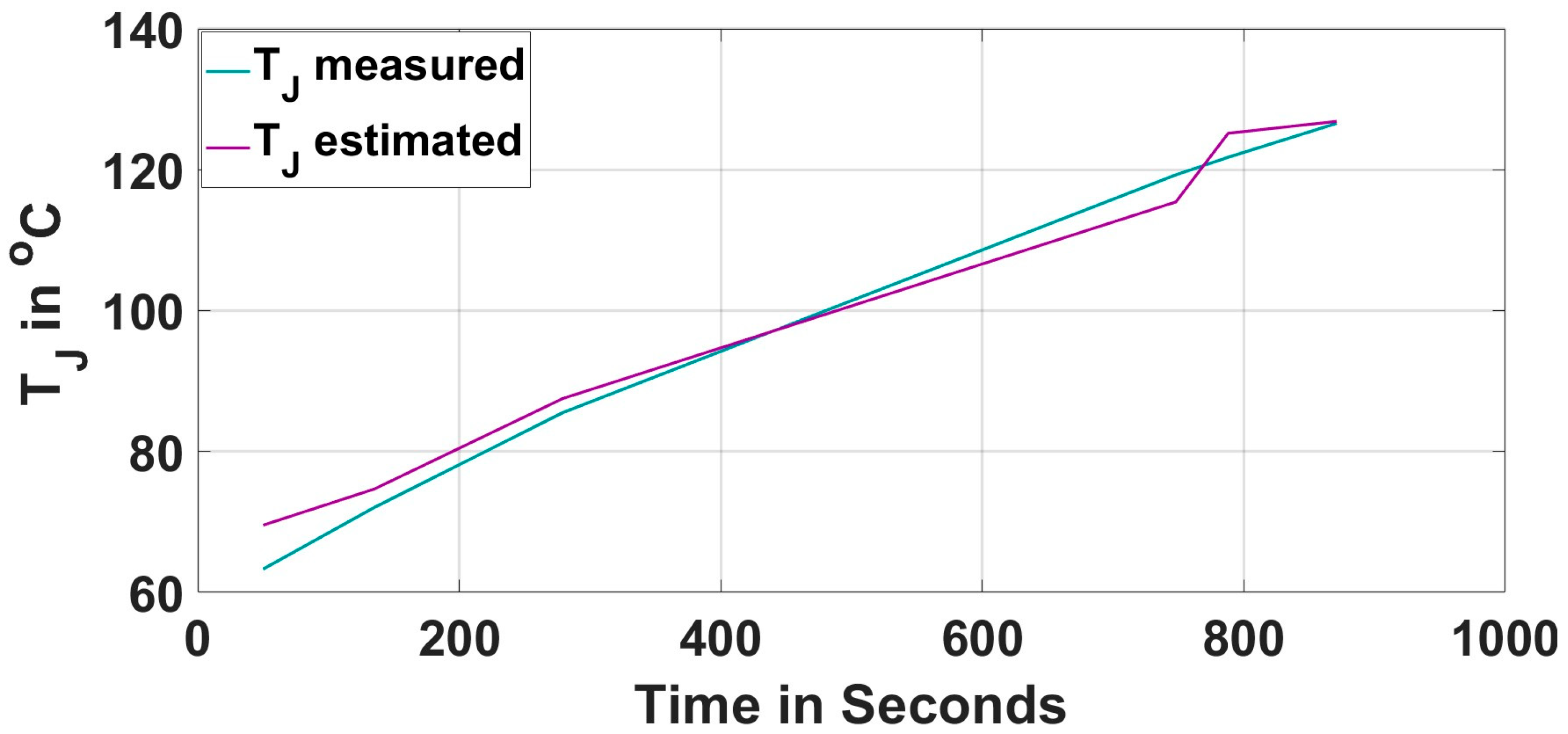
The real-time estimation of the Tj using the Vth is evaluated throughout the operation of the three-phase inverter over a period of 20 min. The inverter has a 500 V DC input and outputs 90 Arms current at 200 Hz. The measured Tj along with the post-processed value of Vth (Vth post-pro) is illustrated in Figure 28. During this test, Tj increases from approximately 30 °C up to 120 °C, while Vth decreases from 2.65 V down to 2.05 V. The measured Vth values are utilized to estimate the Tj based on the look-up table produced with the double-pulse tests. Figure 29 shows the measured and the estimated junction temperatures during the test. Figure 29 validates the effectiveness and the accuracy of the proposed approach for the on-line estimation of the Tj using the Vth measurements, where a maximum divergence of approximately 2~3 °C is found between the estimated and the measured Tj values over a whole duration of the running test of the inverter operation.

5.2. On-Line Tj Estimation Based on the VDSon Measurements

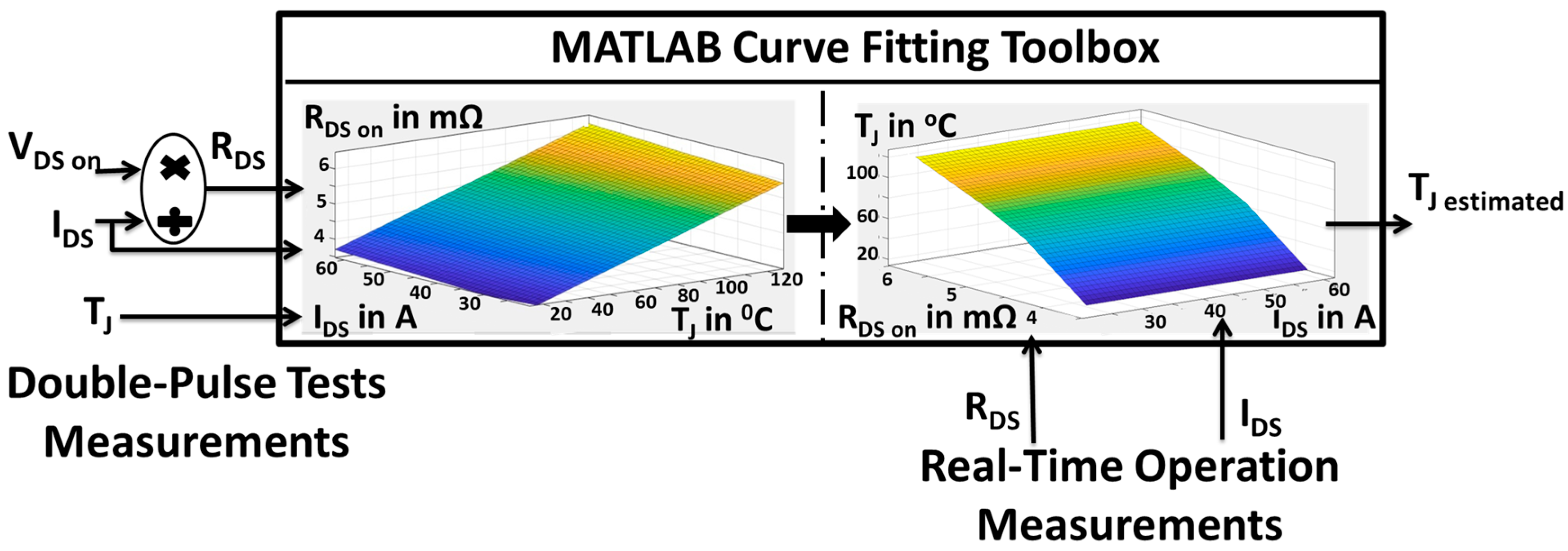
The proposed approach to estimate the Tj using the measurements of VDSon is graphically shown in Figure 30. The off-line double-pulse tests are utilized to generate a 3D look-up table of RDSon = VDSon/IDSon as a function of IDSon and Tj. An inverse look-up table Tj (RDSon,IDSon) is then generated off-line using the MATLAB 2023-a curve-fitting toolbox and utilized afterwards for the on-line estimation process of the Tj. IDSon can be assumed equal to the load current.
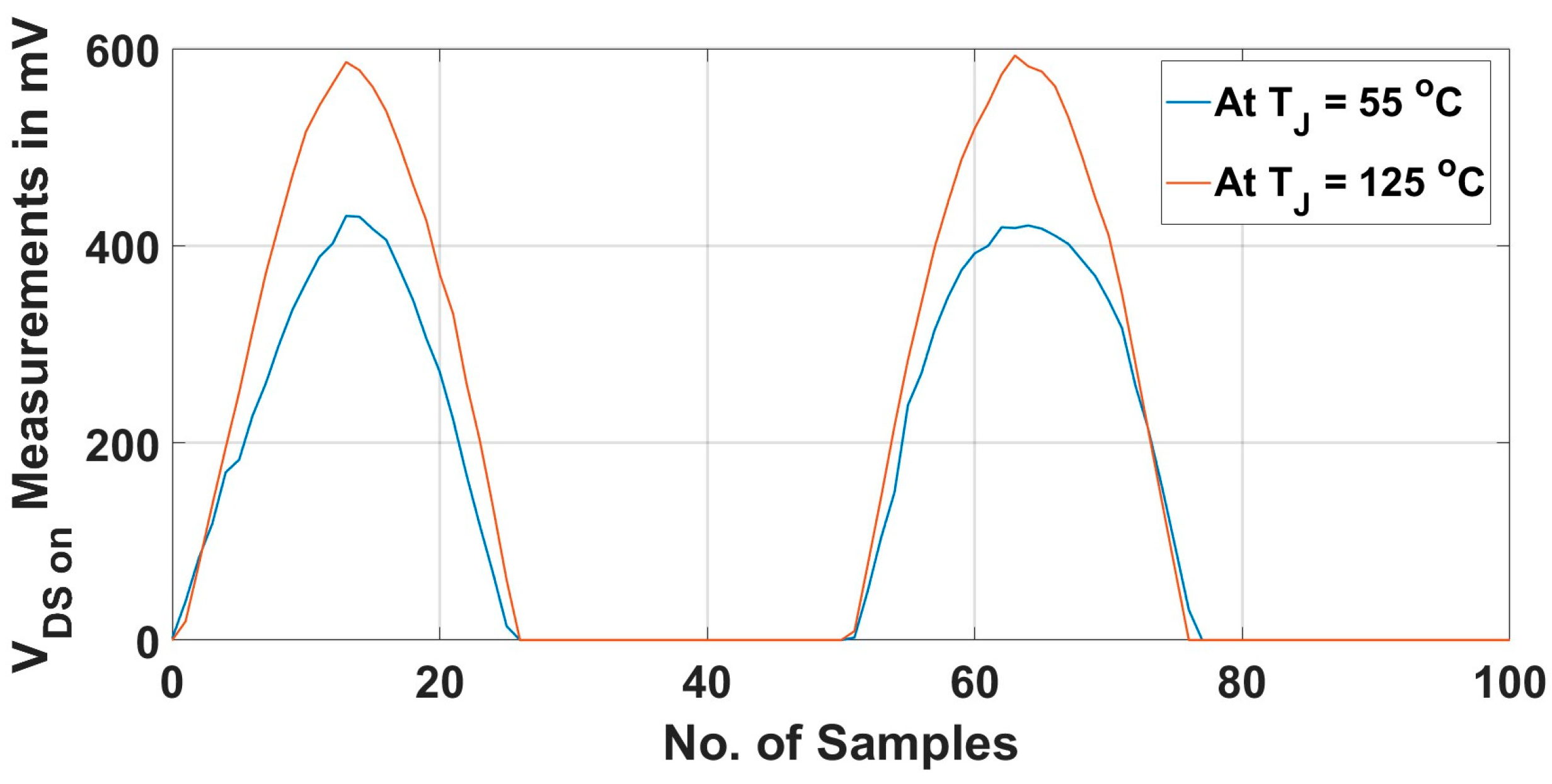
Samples of the real-time measurements of VDSon during the on-line operation of the three-phase inverter are provided in Figure 31 for two different Tj, (55 °C and 125 °C). The waveforms illustrate the sinusoidal pattern of the measured VDSon, which reflects the sinusoidal output phase current during three-phase inverter operation. Only the positive half of the VDSon waveform is captured in the implemented measuring board in this study in order to increase the resolution for utilizing the available input range of the measuring ADC channel.
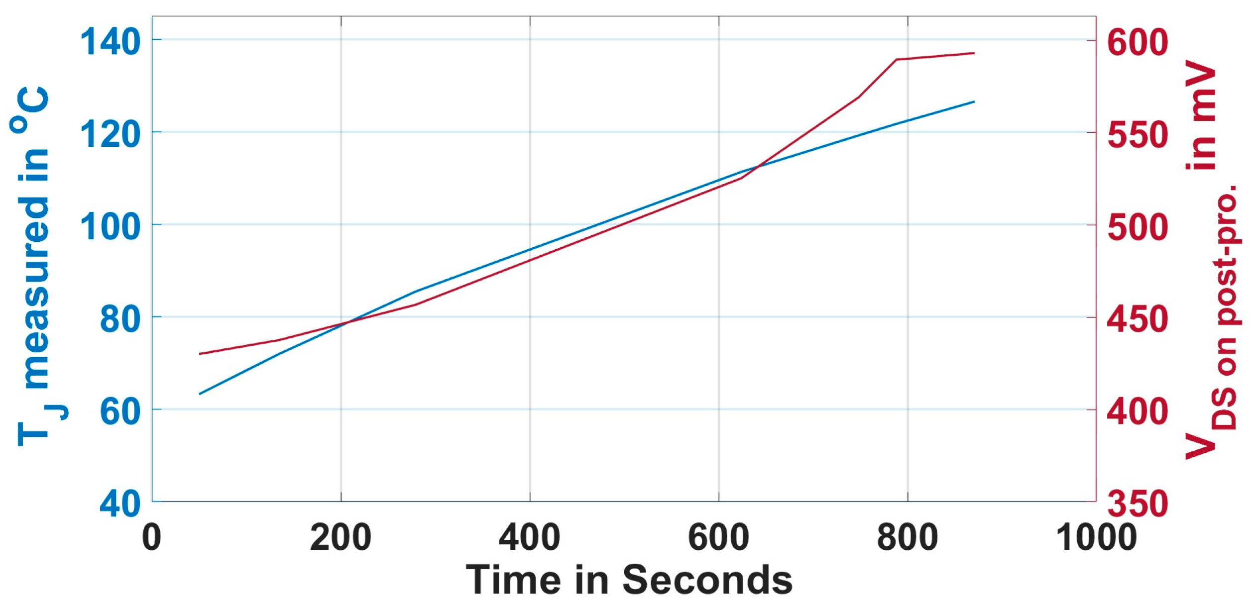
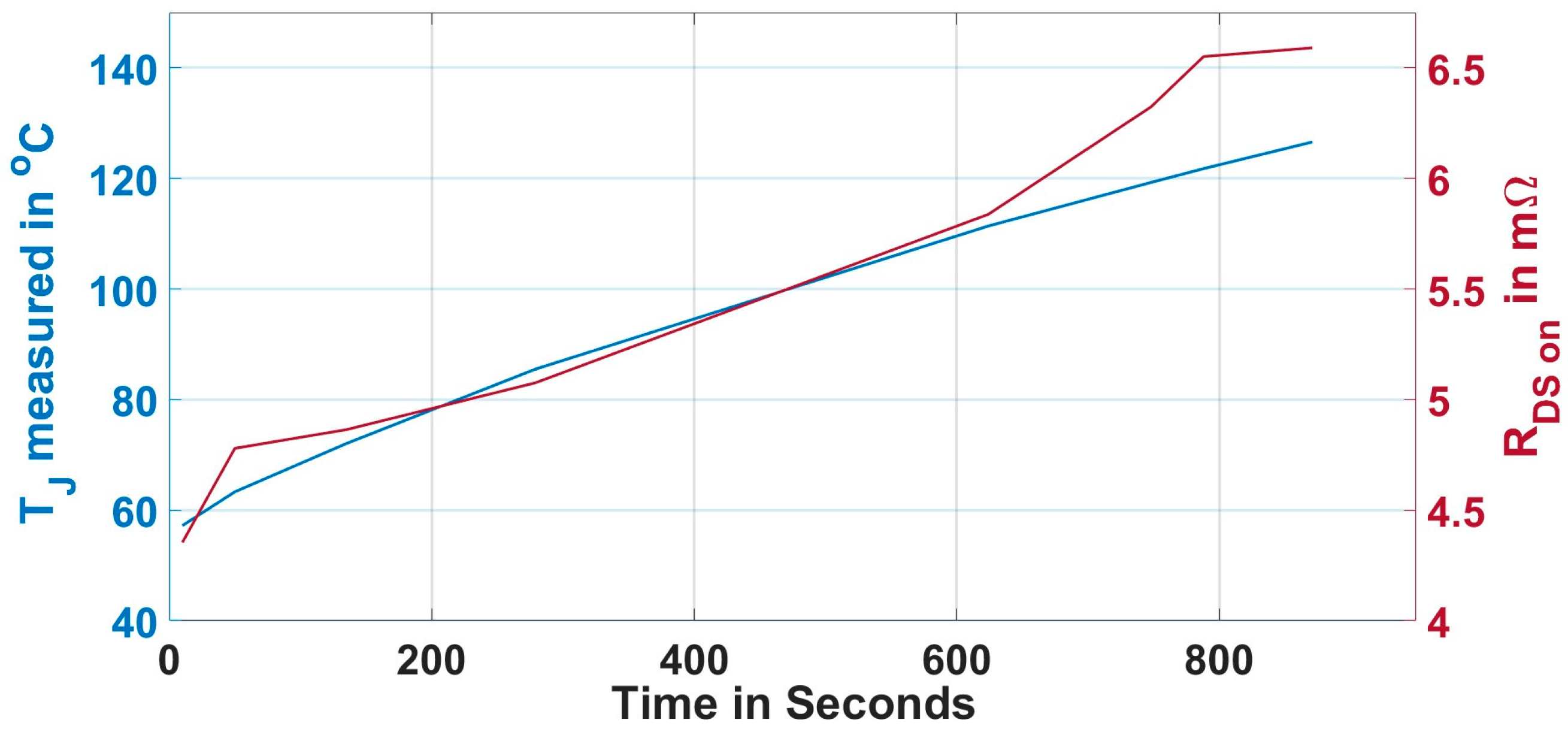
The proposed real-time estimation of Tj is eventually performed as demonstrated in Figure 32. Figure 32 illustrates the measured Tj as well as the post-processed values of VDSon (VDSon post-pro) during the test of the inverter operation at 500 V DC input voltage and 90 Arms, 200 Hz AC output current. During this test, Tj increases from around 60 °C up to 125 °C. Similarly, the VDSon has also increased from approximately 430 mV up to 590 mV. Figure 33 shows the same measured Tj but along with the measured RDSon during the test.
Finally, the measured Tj and the estimated Tj using the developed look-up table Tj (RDSon,IDSon) are compared in Figure 34 and Figure 35 as functions of the experiment time and RDSon, respectively. Accordingly, an advantageous and good Tj estimation has been demonstrated based on the proposed approach of the measurement of the VDSon in this study, where a maximum of 5~6 °C difference took place between the measured and the estimated Tj during the whole running operation period.

5.3. Comparisons Between the TSEPs Under Study

In addition to the common steps that have to carried out to implement both TSEPs under study in modules of parallel-connected chips, Table 4 provides a summary for the differences between these two parameters with respect to their individual requirements for implementation, along with analyses for their performances and feasibilities in modules of parallel-connected chips based on the demonstrated case studies in the paper.
Since the IDS current through one chip is normally not accessible in the majority of the modules of paralleled chips unless an alteration is performed in the module configuration, so it is assumed in this paper that the total IDS current is equally distributed in the parallel chips. However, this could be challenging for the TSEP approach using the VDSon measurement since the current through paralleled chips are varied due to the individual temperature of each chip. Accordingly, based on Table 4 as well as the previous statement, it is shown that the Vth is a better candidate to be utilized for the Tj estimation based on TSEP approach for modules of paralleled chips as it has lower requirements and less estimated error along with better performance and sensitivity compared to the implementation of VDSon as TSEP. As a result, the measurement of Vth is designated to be employed for estimating the Tj of the module under study for the forthcoming reliability modelling and lifetime prediction analysis.

6. Reliability Modelling and Lifetime Prediction

The on-line estimation of the Tj represents the cornerstone to establish the reliability modelling and lifetime prediction for the new designed SiC MOSFET module under study which has been manufactured with the new wire-bond-free planar technology. A lifetime model for the studied module has been developed based on the Rainflow counting analysis using the power cycling tests performed by module manufacture. A mission profile representative of a machine drive operation utilized for aircraft flight has been used to provide a quantification of the estimated lifetime.
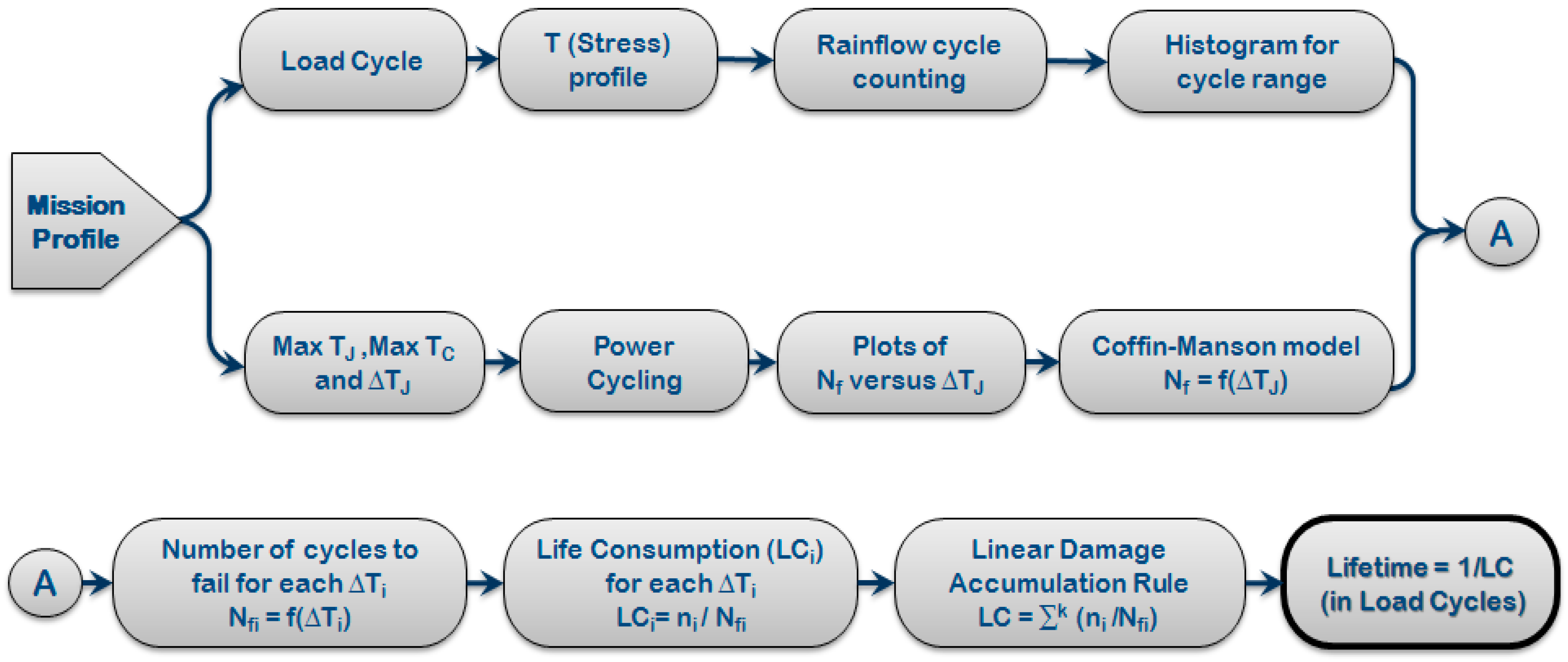
Figure 36 illustrates a flow chart with the steps to perform the proposed lifetime prediction of the SiC MOSFET module. Firstly, for a given mission profile, the estimated Tj profile (as a stress profile) is acquired along with the associated maximum Tj as well as the maximum case temperature (TC). Next, the estimated Tj profile is then processed through the Rainflow cycle counting algorithm to estimate the local maxima and minima (extremes) of the given Tj profile. These extremes are then utilized in the following histogram analysis to evaluate the number of cycles (ni) per amplitude of junction temperature cycles (ΔTj-i) through the Tj profile. On the other hand, power cycling tests have been developed to acquire the numbers of cycles to failure (Nf) for different ΔTj so that the relationship between Nf and the ΔTj could be then achieved based on the Coffin–Manson model [45,46]. As a result, based on the outcomes of the developed histogram analysis as well as the Coffin–Manson model, Nfi for each ΔTj-i is estimated which are used in evaluating the lifetime consumption (LCi) corresponding to each ΔTj-i. Finally, by applying Palmgren–Miner linear damage accumulation rule, the total lifetime consumption (LC) is calculated so that the anticipated lifetime becomes the inverse of the value in load cycle units. These successive steps are demonstrated thoroughly in the following figures.
Based on the defined mission profile, the estimated Tj profile of the module under study is developed as shown in Figure 37. This estimated temperature profile is utilized subsequently in the Rainflow analysis. Rainflow cycle counting algorithm has been performed in order to estimate the local extremes of the developed temperature profile. Figure 38 shows the estimated extremes. The following step is to establish the histogram analysis for these extremes and define for each histogram bin its temperature amplitude (ΔTj-i) as well as the associated number of cycles (ni) for each ΔTj-i. Figure 39 demonstrates the developed histogram analysis for the estimated extremes from the Rainflow algorithm.
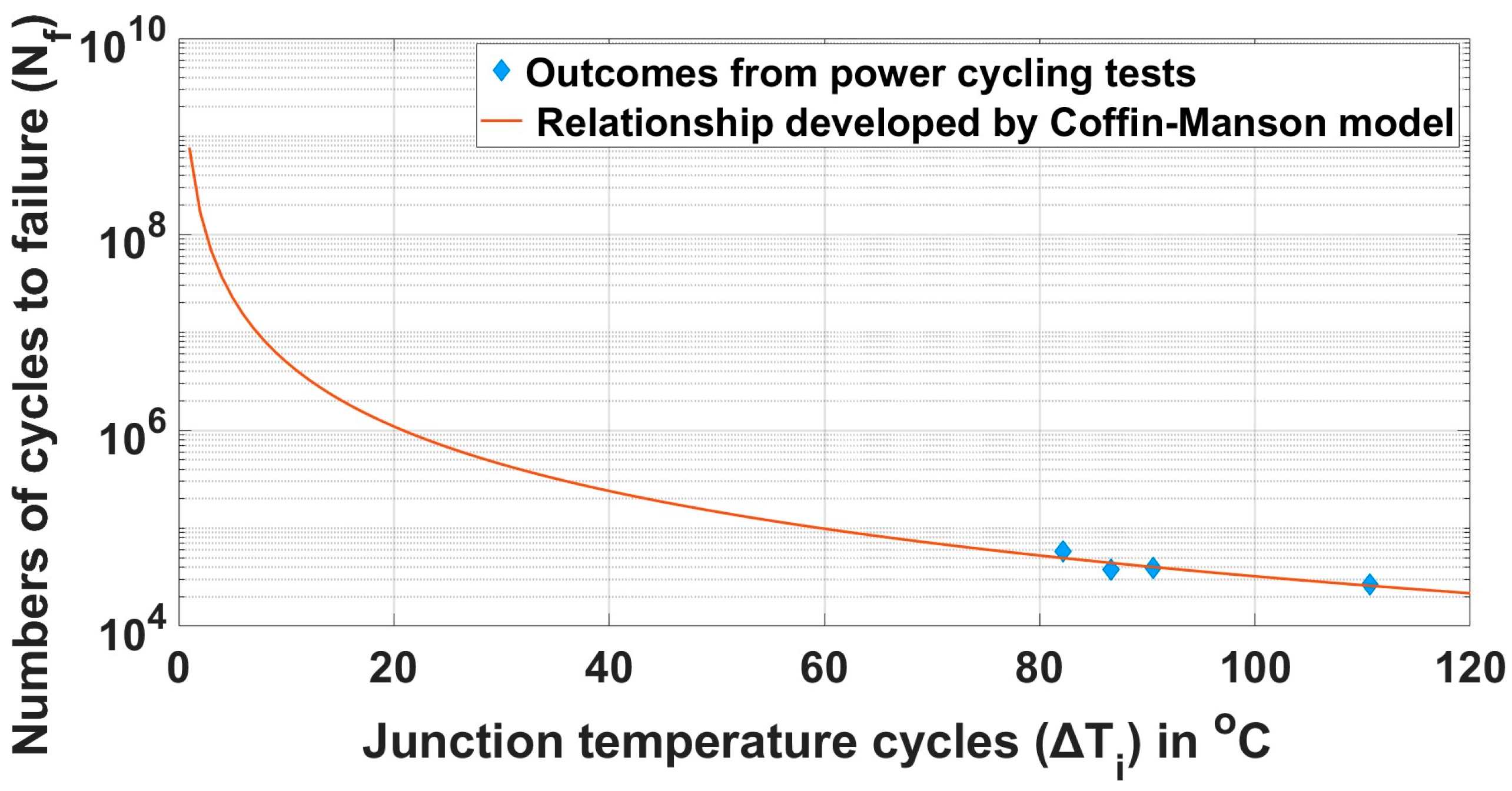
Module manufacture has provided results of power cycling tests for the studied module prototype, so the Nf versus different ΔTj are given at the predefined maxima of Tj and TC. Consequently, the Coffin–Manson model is then developed to evaluate the relationship between Nf and ΔTj where the model coefficients are estimated statistically based on provided data from manufacture power cycling tests.
Figure 40 illustrates the given data from the power cycling tests along with the Coffin–Manson model relating the Nfi and Tj-i as follows:
N f i = k   T j i m
where
k = 7.6854 × 10⁸
m = 2.188
Figure 40. Coffin–Manson Model between Nf and ΔTj.
Machines 13 00689 g040
Table 5 provides the predicted Nfi for each of the defined ΔTi from histogram analysis of Figure 39. It is shown that the predicted Nf, resulted from ΔTj at 80.8 °C, is equal to 5.16 × 10⁴ cycles, while the experimental Nf plotted in Figure 40 at 82.2 °C reached 5.76 × 10⁴ cycles, which gave around 10% variance in such condition.
The final steps towards the evaluation of the lifetime are also demonstrated in Table 5 based on the developed histogram bins in Figure 39 and the estimated Coffin–Manson model in Figure 40. The lifetime consumption (LCi) corresponding to each ΔTj-i in Table 5 is calculated in
L C i = n i N f i
As a result, the total combined lifetime consumption (LC) from the different ΔTj from Table 5 becomes
L C = i n i N f i
where i is from 1 to 4.
Finally, the lifetime is estimated as follows:
l i f e t i m e = 1 L C , in load cycles
Based on the developed reliability model, it is estimated that the device can survive approximately 30,890 load cycles at the specified mission profile which is equivalent to 70,275 flight hours based on the given load cycle of 136.5 min.
In view of that, this section presents how the estimated Tj from the previous sections can be employed to model the reliability of the SiC module under study and predict its lifetime based on a given mission profile. Even though there are other statistical component-level models as given in [47] that can also be adopted to perform the lifetime prediction, they also still require monitoring the Tj as a degradation indicator in real time to update their models’ parameters which were developed in the offline environment.

7. Influence of the Aging of the SIC MOSFETS on the Studied TSEPs

Both TSEPs under study are relatively influenced by the aging effects of the SiC power module in which their values are increasing with the device aging at the same operating Tj due to the gate oxidation degradation that increases the interface trapped charge Qit [48]. On the other hand, to ensure that the degradation tests are representative to the real-world operational conditions as well as the deviations in the TSEP are reflecting only the aging effects, it has to accurately implement the expected environmental factors and conditions that the module will encounter during its lifespan. This involves selecting appropriate accelerated aging techniques, considering environmental factors like temperature, humidity, pressure, electromagnetic interference, etc.
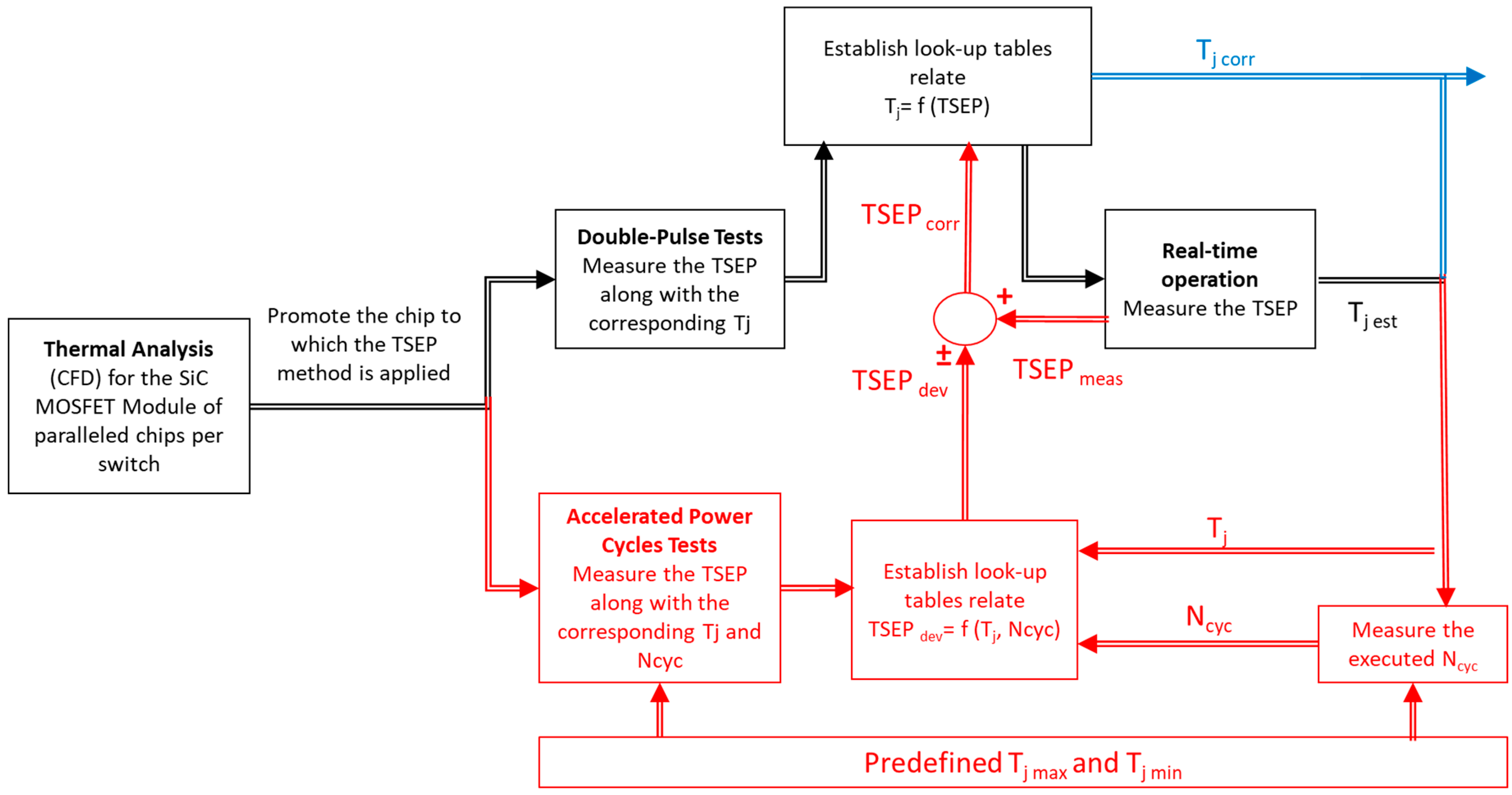
Accordingly, a refinement arrangement is demonstrated in Figure 41 to compensate the divergences in the TSEP under study due to the module degrading effects. This process will include additional accelerated power cycle tests to be applied on the modules under test to correlate the deviations in the TESP under study to Tj as well as to the number of the power cycles (Ncyc) that will be performed on a module till it fails [48]. These accelerated power cycle tests can be applied using sequences of DC or AC power cycle tests till the module under test fails [48,49]. The relationship between the deviations in the TSEP, Tj and Ncyc is established after reaching the failure of one of the modules. This relationship will be then fed to the Ti estimation procedure for other healthy similar modules during its real-time operation in which the number of executed Ncyc will be involved in the estimation process of the Tj to compensate the variations in the TSEP under study due to the module aging effects.
The black route in the illustrated diagram of Figure 39 shows the original procedure for estimating the Tj for the modules of paralleled connected chips without taking into account the deviations in the TSEP under study due to the aging effects of the module. The outcome of this procedure will be denoted as (Tjest). On the other hand, the red route demonstrates the additional refinement process in order to take into consideration the module aging effects in which the number of the executed Ncyc on the module is utilized as well as the estimated Tj to predict the deviation in the TSEP (TSEPdev) based on the look-up tables established by the accelerated power cycle tests. The Ncyc is calculated in this process by defining maximum and minimum boundaries for the Tjest (which are identical to those that are chosen for the accelerated power cycles); consequently, the variation in the Tjest across these boundaries are used to estimate how many Ncyc are executed on the module during its real-time operation. The resultant TSEPdev will then amend the measured TSEP during the real-time operation of the module to evaluate the correct value of the estimated Tj. The outcome of this final process will be labelled as (Tj corr) which will be continuously updated through the refinement procedure of the red route. This proposed refinement procedure is planned to be evaluated in the ongoing future work when additional modules become available from the manufacture side since this module as a new designed prototype is currently under limited availability.

8. Conclusions

This paper presents a systematic procedure to estimate in real time the Tj of the SiC MOSFET modules of paralleled connected chips utilized in the new machine drive systems in order to develop their reliability modelling and predict their lifetime. A measuring board has been designed in this research to capture correctly the TSEP under study: Vth and VDSon, to be used in the on-line estimation of the required Tj. The developed approaches were able to cope with the induced resonances and the parasitic oscillations during the commutation of the parallel chips and captured the correct TSEP values. Both TSEP approaches have then been evaluated and validated in a realistic high power application of a three-phase inverter. It is concluded that both approaches provide adequate sensitivity and linearity between the respective TSEP and the Tj (sensitivity of 5~6.6 mV/°C for Vth and 1~1.45 mV/°C for VDSon). The temperature estimation based on Vth, however, appears simpler in implementation as it does not require output current measurement and it also provides a lower estimation error of 2~3 °C compared to 5~6 °C for VDSon. Eventually, reliability modelling and lifetime prediction was developed for the SiC module under study based on the estimated Tj as well as the power cycle tests provided by the manufacturer. The lifetime has been predicted using Rainflow and histogram analyses under a predefined mission profile representing an aircraft flight. It shows that the module can operate up to 70,275 h which is equivalent to 30,890 cycles of the given load mission profiles. Lastly, a divergence of 2~3 °C in Tj estimation using Vth approach resulted in a maximum deviation of 10% in the predicted lifetime. On the other hand, with a divergence of 5~6 °C in Tj estimation using VDSon approach, a maximum deviation of 17% in the predicted lifetime occurred. Furthermore, based on the available experimental power cycling tests carried out by the module manufacturer, it is shown that the predicted lifetime of 70,275 h is attributed to around 90% confidence level.

Author Contributions

Conceptualization, T.K.; data curation, T.K.; formal analysis, T.J.; investigation, O.O.; methodology, T.K.; project administration, T.J.; resources, T.K., O.O. and T.J.; software, T.K.; supervision, T.J.; validation, T.K. and O.O.; visualization, O.O. and T.J.; writing—original draft, T.K.; writing—review and editing, O.O. and T.K. All authors have read and agreed to the published version of the manuscript.

Funding

This work was supported by European Commission Horizon 2020—Mobility for Growth Program under Grant 636170.

Data Availability Statement

The original contributions presented in the study are included in the article; further inquiries can be directed to the corresponding authors.

Acknowledgments

The authors would like to thank Siemens AG Corporate Technology for providing the SiC MOSFETs module along with its power cycling tests utilized in this paper.

Conflicts of Interest

The authors declare no conflicts of interest.

References

  1. Neeb, C.; Boettcher, L.; Conrad, M.; Doncker, R.W.D. Innovative and reliable power modules: A future trend and evolution of technologies. IEEE Ind. Electron. Mag. 2014, 8, 6–16. [Google Scholar] [CrossRef]
  2. O’Donnell, S.; Debauche, J.L.; Wheeler, P.; Castellazzi, A. Silicon carbide MOSFETs in more electric aircraft power converters: The performance and reliability benefits over silicon IGBTs for a specified flight mission profile. In Proceedings of the EPE’16 ECCE Europe, Karlsruhe, Germany, 5–9 September 2016; pp. 1–10. [Google Scholar]
  3. Oh, H.; Han, B.; McCluskey, P.; Han, C.; Youn, B.D. Physics-of-failure, condition monitoring, and prognostics of insulated gate bipolar transistor modules: A review. IEEE Trans. Power Electron. 2015, 30, 2413–2426. [Google Scholar] [CrossRef]
  4. Wang, H.; Liserre, M.; Blaabjerg, F. Toward reliable power electronics. IEEE Ind. Electron. Mag. 2013, 7, 17–26. [Google Scholar] [CrossRef]
  5. Ciappa, M. Selected failure mechanisms of modern power modules. Microelectron. Rel. 2002, 42, 653–667. [Google Scholar] [CrossRef]
  6. Avenas, Y.; Dupont, L.; Baker, N.; Zara, H.; Barruel, F. Condition monitoring, a decade of proposed techniques. IEEE Ind. Electron. Mag. 2015, 9, 22–36. [Google Scholar] [CrossRef]
  7. Xiong, Y.; Cheng, X.; Shen, Z.J.; Mi, C.; Wu, H.; Garg, V.K. Prognostic and warning system for power-electronic modules in electric, hybrid electric, and fuel-cell vehicles. IEEE Trans. Ind. Electron. 2008, 55, 2268–2276. [Google Scholar] [CrossRef]
  8. Yang, S.; Xiang, D.; Bryant, A.; Mawby, P.; Ran, L.; Tavner, P. Condition monitoring for device reliability in power electronic converters: A review. IEEE Trans. Power Electron. 2010, 25, 2734–2752. [Google Scholar] [CrossRef]
  9. Avenas, Y.; Dupont, L.; Khatir, Z. Temperature measurement of power semiconductor devices by thermo-sensitive electrical parameters—A review. IEEE Trans. Power Electron. 2012, 27, 3081–3092. [Google Scholar] [CrossRef]
  10. Blackburn, D.-L. Temperature measurements of semiconductor devices—A review. In Proceedings of the 20th Annual Semiconductor Thermal Measurement and Management Symposium (SEMI-THERM), San Jose, CA, USA, 11 March 2004; pp. 70–80. [Google Scholar]
  11. Li, C.; Luo, H.; Li, W.; Li, C.; Yang, H.; He, X. Online junction temperature extraction of sic power mosfets with temperature sensitive optic parameter (TSOP) approach. IEEE Trans. Power Electron. 2019, 34, 10143–10152. [Google Scholar] [CrossRef]
  12. Furbock, C.; Thalhammer, R.; Litzenberger, M.; Seliger, N.; Pogany, D.; Gornik, E.; Wachutka, G. A differential backside laserprobing technique for the investigation of the lateral temperature distribution in power devices. In Proceedings of the International Symposium on Power Semiconductor Devices and ICs (ISPSD), Toronto, ON, Canada, 26–28 May 1999; pp. 193–196. [Google Scholar]
  13. Werber, D.; Wachutka, G. Interpretation of laser absorption measurements on 4 H-SiC bipolar diodes by numerical simulation. In Proceedings of the International Conference on Simulation of Semiconductor Processes and Devices (SISPAD), Hakone, Japan, 9–11 September 2008; pp. 89–92. [Google Scholar]
  14. Zarebski, J.; Gorecki, K. The electrothermal large-signal model of powerMOS transistors for SPICE. IEEE Trans. Power Electron. 2010, 25, 1265–1274. [Google Scholar] [CrossRef]
  15. Avenas, Y.; Dupont, L. Comparison of junction temperature evaluations in a power IGBTs module using an IR camera and three thermosensitive electrical parameters. In Proceedings of the 2012 Twenty-Seventh Annual IEEE Applied Power Electronics Conference and Exposition (APEC), Orlando, FL, USA, 5–9 February 2012. [Google Scholar]
  16. Brekel, W.; Duetemeyer, T.; Schilling, O. Time resolved in situ Tvj measurements of 6.5 kV IGBTs during inverter operation. In Proceedings of the Power Conversion Intelligent Motion Conference (PCIM Europe), Nuremberg, Germany, 12–14 May 2009; pp. 806–813. [Google Scholar]
  17. Chen, H.; Ji, B.; Pickert, V.; Cao, W. Real-time temperature estimation for power MOSFETs considering thermal aging effects. IEEE Trans. Device Mater. Rel. 2014, 14, 220–228. [Google Scholar] [CrossRef]
  18. Ccoa, J.A.B.; Strauss, B.; Mitic, G.; Lindemann, A. Investigation of temperature sensitive electrical parameters for power semiconductors (IGBT) in real-time applications. In Proceedings of the Power Conversion Intelligent Motion Conference (PCIM Europe), Nuremberg, Germany, 20–22 May 2014; pp. 1–9. [Google Scholar]
  19. Koenig, A.; Plum, T.; Fidler, P.; Doncker, R.W.D. On-line junction temperature measurement of CoolMOS devices. In Proceedings of the 2007 7th International Conference on Power Electronics and Drive Systems (PEDS), Bangkok, Thailand, 27–30 November 2007; pp. 90–95. [Google Scholar]
  20. Bęczkowski, S.; Ghimre, P.; Vega, A.R.D.; Munk-Nielsen, S.; Rannestad, B.; Thogersen, P. Online Vce measurement method for wearout monitoring of high power IGBT modules. In Proceedings of the 2013 15th European Conference on Power Electronics and Applications, Lille, France, 2–6 September 2013; pp. 1–7. [Google Scholar]
  21. Perpina, X.; Serviere, J.F.; Saiz, J.; Barlini, D.; Mermet-Guyennet, M.; Millan, J. Temperature measurement on series resistance and devices in power packs based on on-state voltage drop monitoring at high current. Microelectron. Rel. 2006, 46, 1834–1839. [Google Scholar] [CrossRef]
  22. Baker, N.; Munk-Nielsen, S.; Iannuzzo, F. Online junction temperature measurement via internal gate resistance during turn-on. In Proceedings of the 2014 16th European Conference on Power Electronics and Applications, Lappeenranta, Finland, 26–28 August 2014; pp. 1–10. [Google Scholar] [CrossRef]
  23. Baker, N.; Munk-Nielsen, S.; Iannuzzo, F.; Liserre, M. IGBT junction temperature measurement via peak gate current. IEEE Trans. Power Electron. 2016, 31, 3784–3793. [Google Scholar]
  24. Griffo, A.; Wang, J.; Colombage, K.; Kamel, T. Real-time measurement of temperature sensitive electrical parameters in sic power MOSFETs. IEEE Trans. Ind. Electron. 2018, 65, 2663–2671. [Google Scholar] [CrossRef]
  25. Jiang, X.; Jiang, X.; Wang, J.; Yu, H.; Chen, J.; Zeng, Z.; Yang, X.; Shen, Z.J. Online Junction Temperature Measurement for SiC MOSFET Based on Dynamic Threshold Voltage Extraction. IEEE Trans. Power Electron. 2021, 36, 3757–3768. [Google Scholar] [CrossRef]
  26. Stella, F.; Pellegrino, G.; Armando, E.; Daprà, D. Online junction temperature estimation of SIC power MOSFTES through on-state voltage mapping. IEEE Trans. Ind. Appl. 2018, 54, 3453–3462. [Google Scholar] [CrossRef]
  27. Wang, X.; Zou, M.; Gong, J.; Wang, Y.; Zeng, Z. Junction Temperature Monitoring of GaN HEMT by Using On-Resistance with Voltage Clamp and Current Shunt. In Proceedings of the 2025 IEEE Applied Power Electronics Conference and Exposition (APEC), Atlanta, GA, USA, 16–20 March 2025; pp. 219–224. [Google Scholar]
  28. Niu, H.; Lorenz, R.D. Real-time junction temperature sensing for silicon carbide MOSFET with different gate drive topologies and different operating conditions. IEEE Trans. Power Electron. 2018, 33, 3424–3440. [Google Scholar] [CrossRef]
  29. Yang, F.; Pu, S.; Xu, C.; Akin, B. Turn-on delay based real-time junction temperature measurement for SiC MOSFETs with aging compensation. IEEE Trans. Power Electron. 2021, 36, 1280–1294. [Google Scholar] [CrossRef]
  30. Peftitsis, D.; Baburske, R.; Rabkowski, J.; Lutz, J.; Tolstoy, G.; Nee, H.-P. Challenges regarding parallel connection of SiC JFETS. IEEE Trans. Power Eletron. 2013, 28, 4526. [Google Scholar] [CrossRef]
  31. Hu, J.; Alatise, O.; González, J.A.O.; Bonyadi, R.; Ran, L.; Mawby, P.A. The effect of electrothermal nonuniformities on parallel connected SIC power devices under unclamped and clamped inductive switching. IEEE Trans. Power Electron. 2016, 31, 4526–4535. [Google Scholar] [CrossRef]
  32. Tiwari, S.; Rabiei, A.; Shrestha, P.; Midtgård, O.-M.; Undeland, T.M.; Lund, R. Design considerations and laboratory testing of power circuits for parallel operation of silicon carbide MOSFETs. In Proceedings of the 2015 (EPE’15 ECCE-Europe), Geneva, Switzerland, 8–10 September 2015; pp. 1–10. [Google Scholar]
  33. Sadik, D.; Colmenares, J.; Peftitsis, D.; Lim, J.; Rabkowski, J.; Nee, H. Experimental investigations of static and transient current sharing of parallel-connected silicon carbide MOSFETs. In Proceedings of the 2013 15th European Conference on Power Electronics and Applications (EPE), Lille, France, 2–6 September 2013; pp. 1–10. [Google Scholar]
  34. Aichinger, T.; Rescher, G.; Pobegen, G. Threshold voltage peculiarities and bias temperature instabilities of SiC MOSFETs. Microelectron. Reliab. 2018, 80, 68–78. [Google Scholar] [CrossRef]
  35. Peters, D.; Aichinger, T.; Basler, T.; Rescher, G.; Puschkarsky, K.; Reisinger, H. Investigation of threshold voltage stability of SiC MOSFETs. In Proceedings of the 2018 IEEE 30th International Symposium on Power Semiconductor Devices and ICs (ISPSD), Chicago, IL, USA, 13–17 May 2018; pp. 40–43. [Google Scholar]
  36. Jooq, M.K.Q.; Miralaei, M.; Ramezani, A. Post-layout simulation of an ultra-low-power OTA using DTMOS input differential pair. Int. J. Electron. Lett. 2017, 6, 168–180. [Google Scholar] [CrossRef]
  37. Gonzalez, J.A.O.; Alatise, O. A Novel non-intrusive technique for BTI characterization in SiC MOSFETS. IEEE Trans. Power Electron. 2019, 34, 5737–5747. [Google Scholar] [CrossRef]
  38. Luo, H.; Chen, Y.; Sun, P.; Li, W.; He, X. Junction temperature extraction approach with turn-off delay time for high-voltage high-power IGBT modules. IEEE Trans. Power Electron. 2016, 31, 5122–5132. [Google Scholar] [CrossRef]
  39. Dodge, J. Eliminating Parasitic Oscillation Between Parallel MOSFETs; Advanced Power Technology Application Note APT-0402; Advanced Power Technology: Lafayette, IN, USA, 2004. [Google Scholar]
  40. Joffe, E.B.; Lock, K.S. Grounds for Grounding: A Circuit to System Handbook; Wiley-IEEE: Hoboken, NJ, USA, 2010; Chapter 9. [Google Scholar]
  41. Wei, R.; Song, S.; Yang, K.; Cui, Y.; Peng, Y.; Chen, X.; Hu, X.; Xu, X. Thermal conductivity of 4H-SiC single crystals. J. Appl. Phys. 2013, 113, 053503. [Google Scholar] [CrossRef]
  42. Chen, M.; Wang, H.; Pan, D.; Wang, X.; Blaabjerg, F. Thermal characterization of silicon carbide MOSFET module suitable for high-temperature computationally efficient thermal-profile prediction. IEEE J. Emerg. Sel. Top. Power Electron. 2021, 9, 3947–3958. [Google Scholar] [CrossRef]
  43. Ordonez-Miranda, J.; Hermens, M.; Nikitin, I.; Kouznetsova, V.G.; van der Sluis, O.; Ras, M.A.; Reparaz, J.; Wagner, M.; Sledzinska, M.; Gomis-Bresco, J.; et al. Measurement and modeling of the effective thermal conductivity of sintered silver pastes. Int. J. Therm. Sci. 2016, 108, 185–194. [Google Scholar] [CrossRef]
  44. CREE. Silicon Carbide Power MOSFET C2MTM MOSFET Technology N-Channel Enhancement Mode C2M0025120D Datasheet. Rev. B, October 2015. Available online: https://docs.rs-online.com/3ef6/0900766b8149fd3d.pdf (accessed on 1 July 2025).
  45. Coffin, L.F., Jr. A study of the effects of cyclic thermal stresses on a ductile metal. Trans. Am. Soc. Mech. Eng. 1954, 76, 931–949. [Google Scholar] [CrossRef]
  46. Musallam, M.; Yin, C.; Bailey, C.; Johnson, M. Mission profile-based reliability design and real-time life consumption estimation in power electronics. IEEE Trans. Power Electron. 2015, 30, 2601–2613. [Google Scholar] [CrossRef]
  47. Ni, Z.; Lyu, X.; Yadav, O.P.; Singh, B.N.; Zheng, S.; Cao, D. Overview of real-time lifetime prediction and extension for SiC power converters. IEEE Trans. Power Electron. 2020, 35, 7765–7794. [Google Scholar] [CrossRef]
  48. Ugur, E.; Yang, F.; Pu, S.; Zhao, S.; Akin, B. Degradation assessment and precursor identification for SiC MOSFETs under high temp cycling. IEEE Trans. Ind. Appl. 2019, 55, 2858–2867. [Google Scholar] [CrossRef]
  49. Choi, U.; Blaabjerg, F.; Jørgensen, S. Power cycling test methods for reliability assessment of power device modules in respect to temperature stress. IEEE Trans. Power Electron. 2017, 33, 2531–2551. [Google Scholar] [CrossRef]
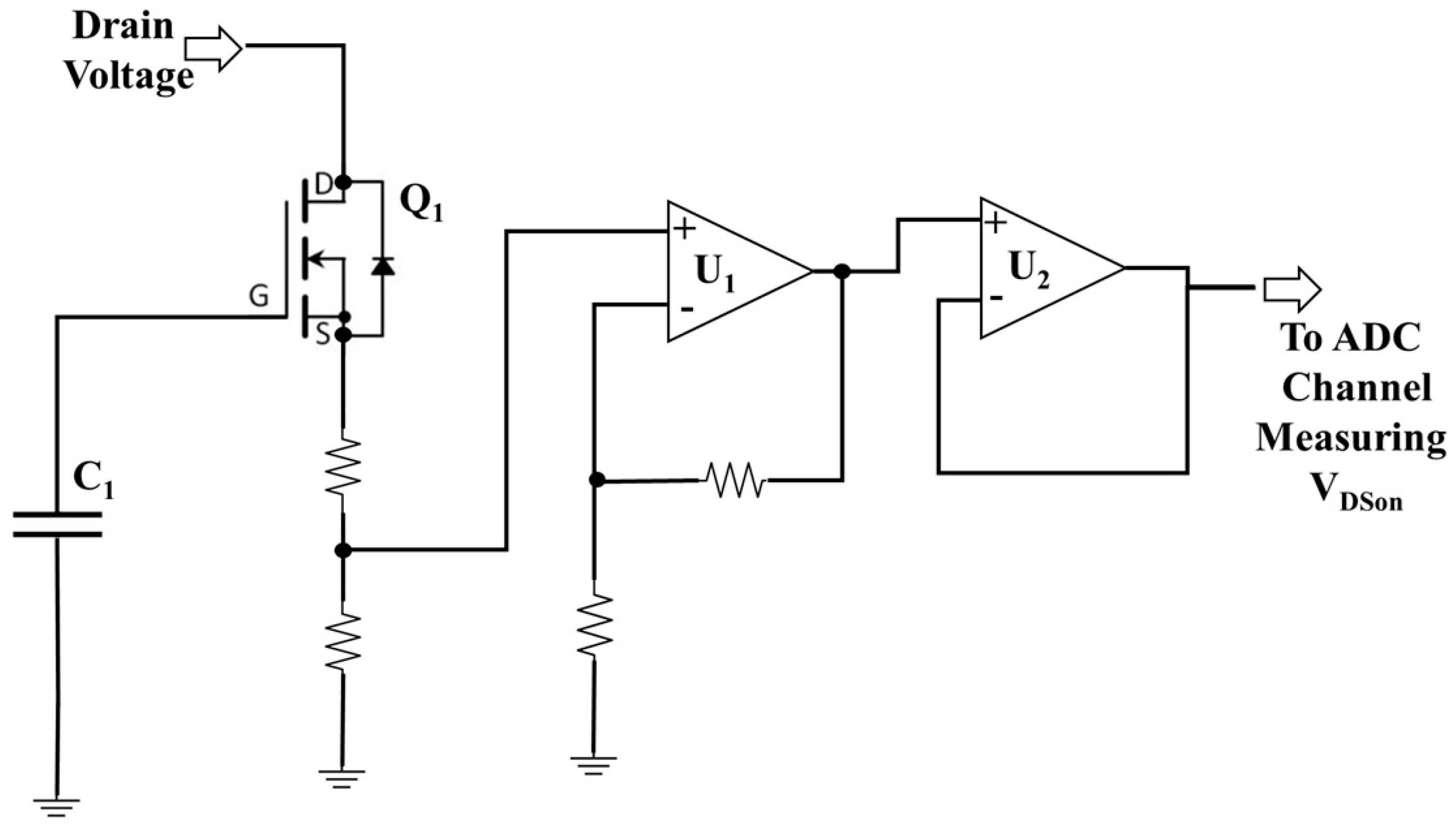
Figure 1. Schematic circuit for VDSon measurement.
Machines 13 00689 g001
Figure 2. Schematic circuit for triggering the ADC channel for the Vth measurement.
Machines 13 00689 g002
Figure 3. Flow chart of the proposed methodical procedure to estimate in real time the Tj of SiC modules, of paralleled chips, for development of their reliability modelling and lifetime prediction.
Machines 13 00689 g003
Figure 4. SiC Power MOSFET module under the study.
Machines 13 00689 g004
Figure 5. CAD drawings of the SiC Power MOSFET module under study.
Machines 13 00689 g005
Figure 6. CFD thermal analysis layout for the SiC Power MOSFET module under the study.
Machines 13 00689 g006
Figure 7. Experimental setup for the double-pulse test.
Machines 13 00689 g007
Figure 8. Schematic circuit for SiC MOSFET Module in double-pulse tests under the study.
Machines 13 00689 g008
Figure 9. The VGS and Vtrig1 measurements at 100 °C Tj.
Machines 13 00689 g009
Figure 10. The VGS and Vtrig1 measurements at 20 °C Tj.
Machines 13 00689 g010
Figure 11. Acquired Vth by the ADC channel at 100 °C Tj.
Machines 13 00689 g011
Figure 12. Acquired Vth by the ADC channel at 20 °C Tj.
Machines 13 00689 g012
Figure 13. Acquired VDSon by the ADC channel at 100 °C Tj.
Machines 13 00689 g013
Figure 14. Acquired VDSon by the ADC channel at 20 °C Tj.
Machines 13 00689 g014
Figure 15. The gate driver adapter board with the cut-out.
Machines 13 00689 g015
Figure 16. The temperature measurements for the three visible dies through the cut-out in the gate driver adaptor board.
Machines 13 00689 g016
Figure 17. Thermal camera temperature measurement at 19 °C Tj. (a) Experimental setup and (b) boxplot for the temperature measurements.
Machines 13 00689 g017
Figure 18. Thermal camera temperature measurement at 122 °C Tj. (a) Experimental setup and (b) boxplot for the temperature measurements.
Machines 13 00689 g018
Figure 19. Double-pulse test waveforms at 19 °C Tj.
Machines 13 00689 g019
Figure 20. Captured samples of the TSEP under study at Tj = 90 °C, (a) captured Vth samples at IO equals 20 A, 40 A, 60 A, (b) captured VDSon samples at IO equals 20 A, (c) captured VDSon samples at IO equals 40 A and (d) captured VDSon samples at IO equals 60 A.
Machines 13 00689 g020
Figure 21. Fitted normal distribution function for the captured samples of Vth in Figure 20a.
Machines 13 00689 g021
Figure 22. Some results of double-pulse test for VDSon.
Machines 13 00689 g022
Figure 23. Some results of double-pulse test for Vth.
Machines 13 00689 g023
Figure 24. Three-phase inverter circuit layout.
Machines 13 00689 g024
Figure 25. Schematic circuit for SiC MOSFET Module in the three-phase inverter.
Machines 13 00689 g025
Figure 26. VGS of the lower side switches of the three-phase inverter and VS’S of the switch of the leg1.
Machines 13 00689 g026
Figure 27. (a) VGS Low leg 1 measured by the ADC channel of the measuring board. (b) filtered and post-processed Vth measurements.
Machines 13 00689 g027
Figure 28. Measured Tj and Vth post-pro during the operation of the inverter at 500 V input DC and 90 AC output current.
Machines 13 00689 g028
Figure 29. Measured and estimated Tj.
Machines 13 00689 g029
Figure 30. Estimation of the Tj using the VDSon measurements.
Machines 13 00689 g030
Figure 31. VDSon measurement samples at two different Tj during the operation of the three-phase inverter.
Machines 13 00689 g031
Figure 32. Estimated Tj and measured VDSon post-pro.
Machines 13 00689 g032
Figure 33. Estimated Tj and measured RDson.
Machines 13 00689 g033
Figure 34. Measured and estimated Tj during the experiment time.
Machines 13 00689 g034
Figure 35. Measured and estimated Tj as function of RDSon.
Machines 13 00689 g035
Figure 36. Architecture for development of the reliability modelling and lifetime prediction.
Machines 13 00689 g036
Figure 37. Estimated Tj versus time during 136.5 min of operation.
Machines 13 00689 g037
Figure 38. Rainflow cycles of the estimated Tj profile.
Machines 13 00689 g038
Figure 39. Histogram showing number of cycles (ni) per amplitude of ΔTj-i
Machines 13 00689 g039
Figure 41. The original procedure (in black route) and refinement process (in red route) to estimate the Tj using TSEP approach for modules of paralleled chips per switch.
Machines 13 00689 g041
Table 1. Measurement approaches of junction temperature.
ApproachCommentsMethodReference
OpticalRequires the chip to be optically connected to the detection system and therefore the protective dielectric gel has to be removedElectroluminescence of MOSFET
body diode
[11]
Laser deflection[12,13]
Infrared radiation[14,15]
Physical contactRequires significant alterations to module packaging and dielectric gel to place the device as close as possible to the chipThermo-sensitive devices
such as thermistors or thermocouples
[16]
TSEPProvides a more practical solution for temperature monitoring since they rely on the thermal dependence of the electrical properties of the semiconductor devices to determine the Tj without modification to the module itselfThreshold
voltage (Vth)
(i) 
Good sensitivity with negative slope linearity over a wide operational range.
(ii)
Auxiliary Kelvin source measurement is required.
[17,18]
On-state
Voltage
(VDSon)
(i) 
Good sensitivity with positive slope linearity over a wide operational range.
(ii)
Current dependent.
[19,20,21]
Internal gate
resistance (Rg)
(i) 
High-resolution ADC is required due to its low temperature sensitivity.
(ii)
Highly vulnerable to EMI
[22,23]
Table 2. TSEP implementation for SIC power MOSFETS.
PaperFeaturesDrawbacks
[24]Quantifies the characteristics of some TSEP including Vth, VDSon, the turn-on transient characteristic (di/dt)The quantification procedures took place only during the double-pulse test process and have not been verified in real-world operation scenarios
[25]On-line junction temperature measurement for SiC MOSFET based on Vth extractionThe proposed Vth measurement is experimentally evaluated only through the double-pulse tests, not during real-world operation scenarios as well
[26]Provides on-line junction temperature estimation using VDSonIt required a thermistor embedded in the module to measure the DBC temperature along with a shunt resistor in series with the switch to measure its current
[27]Junction temperature monitoring using on-resistance with voltage clamp and current shunt It required high bandwidth shunt approach integrated in the PCB board to detect the drain current
[28]Utilizes the gate drive current (ig) during turn-on transients to estimate the TjThe proposed approaches have high sensing offset 9–12 °C for Tj. In addition, they cannot directly regulate ig during the turn-on transient
[29]Real-time junction temperature measurement for SiC MOSFETs using turn-on delay approachIt required sophisticated adjustable gate resistance circuit along with high resolution capture device to ensure proper results
Table 3. Components of the three-phase inverter.
ComponentsDescription/Values
MOSFET module (M1)SiC MOSFET Module under study
MOSFET module (M2 and M3)CREE CAS300M12BM2
DC Link Capacitor (C1)600 µF Film capacitor
Module mounted Capacitors
(C2, C3, C4)
2.2 µF Polypropylene
Load Inductor (L)3 Phase 320 µH Inductor
Current sensorsLEM LF 205-S
Gate Driver BoardsProdrive PT62SCMD12
Table 4. Comparisons between Vth and VDSon as TSEP based on the demonstrated case studies.
VthVDSon
Requirements
  • The VS’S measurement to trigger the measuring ADC channel for the Vth
  • The VS’S measurement to trigger the measuring ADC channel for VDS after a predefined time delay
  • Additional high voltage switch is required to block the high turn-off voltage from the measuring circuit
  • Additional current sensor to measure the IDS current through the chip to which the TSEP method is applied (1)
DependentsTemperatureTemperature and IDS current
Performance
  • Linear with negative slope characteristics
  • Sensitivity of 5~6.6 mV/°C
  • Semi-linear with positive slope characteristics
  • Sensitivity of 1~1.45 mV/°C
Estimated errorMaximum divergence of 2~3 °C between the estimated and the measured TjMaximum divergence of 5~6 °C between the estimated and the measured Tj
(1) Not applicable in most of the modules of paralleled chips per switch.
Table 5. Life consumption and lifetime evaluation for the module under study.
Ti5.22255.680.8
ni312.50.5
Nfi2.08 × 1078.88 × 1051.17 × 1055.16 × 104
LCi1.44 × 10−71.13 × 10−62.14 × 10−59.70 × 10⁻⁶
LCtotal3.2373 × 10−5
Lifetime30,890 (load cycles) ≈ 70,275 h
Disclaimer/Publisher’s Note: The statements, opinions and data contained in all publications are solely those of the individual author(s) and contributor(s) and not of MDPI and/or the editor(s). MDPI and/or the editor(s) disclaim responsibility for any injury to people or property resulting from any ideas, methods, instructions or products referred to in the content.