Abstract
This article explores the issue of surface modification through tumbling and vaporisation of 3D-printed materials, and its impact on the electrolytic deposition of metal coatings on previously non-conductive materials. Plastic materials represent an affordable alternative, but their surface treatment, in the form of post-coating, achieves properties comparable to those of metal parts while saving expensive metal material. Samples prepared by selective laser sintering (SLS) with different surface treatments were used. Polyamide 12 (PA12) was chosen as the base material and copper (Cu) as the metallic coating. Graphite was sprayed on the samples to ensure conductivity. The Cu coating was electrodeposited from an acidic copper electrolyte. The quantitative analysis of the surface was carried out using standard ISO parameters. The thickness of the deposited copper layer was determined using destructive measurements on a digital microscope. The results show that surface modification has a significant effect on the functional properties of the surface quality and the thickness of the deposited copper layer.
1. Introduction
With increasing demands for precision, functionality, and repeatability, the need for advanced process control and optimisation is also growing, while the emphasis remains on economical manufacturing. The search for new manufacturing approaches that can reduce costs and shorten product development times has led to the intensive development of additive manufacturing. In recent years, additive manufacturing (AM) has experienced dynamic development across all industrial sectors. The widespread acceptance of 3D printing technology stems from its ability to produce complex geometries with reduced production times [1]. The main advantages of AM include design flexibility, the low weight of prints, minimisation of material waste, and the possibility of personalisation, which make it an attractive alternative to conventional manufacturing methods [2,3,4]. One of the most widespread and most commercially used additive manufacturing methods is selective laser sintering (SLS), which works on the principle of gradually sintering polymer powder layer by layer [5,6]. This technology is widely applied, especially in printing nylon materials, such as PA12, PA11, or Alumide, which are characterised by low density, high chemical resistance, dimensional stability, and, last but not least, favourable production costs [7,8].
The disadvantage of printed parts made from nylon materials is their susceptibility to damage when exposed to atmospheric ageing, temperature fluctuations, humidity, and ultraviolet (UV) radiation in outdoor conditions [9]. To expand the application potential of 3D-printed parts, it is necessary to ensure the required mechanical properties while maintaining the geometric parameters of the parts. The solution is to apply a metal layer to the polymer part. This process is called metallization. This creates new application potential, for example, in the fields of electrical engineering or the automotive industry. Since plastics such as polyamide 12 (PA12) are naturally non-conductive, surface modification is necessary prior to electrochemical metallization to improve their adhesion and enable conductive connection with the electrolyte. Proven methods include the application of a graphite interlayer, plasma activation, or mechanical and chemical surface treatment [10,11]. However, polymer parts lack the properties that metals have. One of the most effective approaches to achieving these properties is electroplating, which enables a metal coating to be applied to non-conductive polymer substrates, thereby obtaining properties comparable to those of metal components while retaining the advantages of a lightweight plastic core [12,13,14]. Electroplating techniques allow for the incorporation of fillers, such as carbon black, graphite, carbon nanotubes, metallic fibers, and others [15]. The metallization process can be carried out through direct or electroless plating, vacuum deposition, or sputtering using various metals, such as copper, silver, gold, and nickel. Zinc can also be used for coating applications [16,17,18]. This method was investigated by Islam et al. [19], who reported that achieving complete metal coverage on plastic surfaces via electroplating is challenging, yet feasible. They also emphasised that the surface preparation prior to metal deposition significantly influences the quality and uniformity of the resulting metal coating.
The surface quality of 3D-printed parts fundamentally affects the resulting mechanical, electrical, and functional properties of the electroplated layer. Uneven surface topography can lead to poor metal adhesion, reduced conductivity, or reduced mechanical resistance of the components, which is especially important for applications in the electrical or automotive industries. Recent studies show that the key factor for successful plating is the surface topography, which is quantified by roughness parameters and their influence on the distribution of electrolytes and the quality of the deposited layer [20,21]. For example, the work of the authors [22] confirms that vaporisation as a post-process treatment significantly reduces peak irregularities and contributes to increasing the uniformity of the metal coating. Finally, the quantitative evaluation of the resulting layer is also important, as destructive measurement allows for the study of individual layers using a microscope [23].
The present study examined the impact of surface treatment on the quality of the electroplated copper layer on 3D PA12 components. The aim was to identify a technological process that will lead to the formation of a compact layer on the plated surface and to monitor the effect of surface modification using height and areal stratification parameters of surface roughness. The electroplating process requires little equipment. Another advantage of SLS over other plating options for electronic applications, such as electronic circuit carriers with complex shapes, is that it can be manufactured, and conductors can be replaced by selectively deposited copper channels.
To achieve optimal properties of the plated surface, surface modifications by tumbling and vaporisation were tested. Tumbling is a mechanical process in which abrasive media remove surface irregularities and simultaneously reduce surface roughness. It results in a unified, textured surface with better conditions for adhesion of the electroplated metal. Vaporisation is a chemical–physical process in which the surface of the material treated by steam is provided with solvent vapor or other substances. This method enables a smoother and more homogeneous surface to be achieved, which can impact the uniformity of the subsequent plating. According to recent publications, surface preparation is one of the main factors affecting the quality and integrity of the Cu coating [24,25]. The overall results indicate the use of pretreatment in the subsequent use of 3D-printed products, with an emphasis on the time and cost of the production process.
2. Materials and Methods
2.1. Experimental Setup
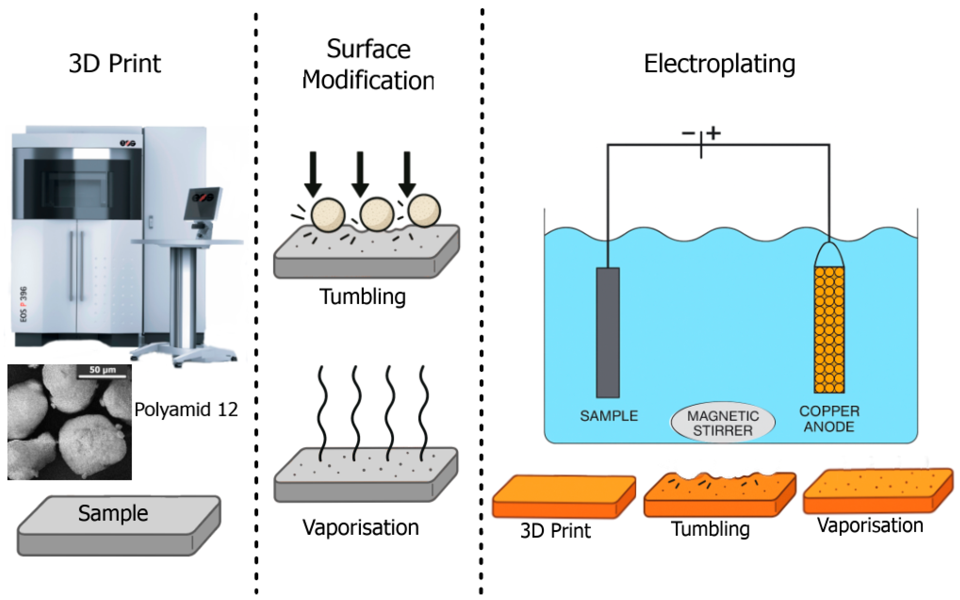
The experimental setup is depicted in Figure 1, describing the process of 3D printing through surface modification to electroplating. The EOS P396 3D printer (Robertstirlingring, Krailling, Germany) was used for the production of samples (dimensions: 20 × 60 × 2 mm). It is equipped with a laser with a maximum nominal power of 70 W. The machine has a build volume of 340 × 340 × 620 mm3 and a scanning speed of up to 6 m⋅s−1. The powder used is intended for producing functional prototypes via laser powder bed fusion (L-PBF) technology. It is not virgin powder, but a 50:50 mixture of new and previously used powder of the same type. This mixing ratio, known as the refresh factor, is recommended by the manufacturer [26]. The printing parameters used were as follows: a layer thickness of 120 µm, a process chamber temperature of 171 °C, and a removal chamber temperature of 130 °C. The beam offset was set to 0.33 mm. Material-dependent scaling was applied, with values of 3.15% in the X direction, 3.23% in the Y direction, 1.4% in the Z direction at 0 mm height, and 2.55% in the Z direction at 600 mm height.
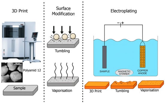
Figure 1.
Experimental Setup: 3D Print, Surface Modification, Electroplating.
One of the most tested materials for additive manufacturing, commercial PA12 powder (EOS PA2200; EOS GmbH, Krailling, Germany.), was used as the experimental material for sample production. The particle size distribution was determined using a microscope in the range of 40–75 µm. The particles have a spherical shape. Furthermore, smaller parts were observed to be attached to larger parts. This phenomenon may be caused by electrostatic forces generated during the regeneration of PA12 powder when recycled and fresh powder are mixed [27].
The surface treatment was performed using tumbling technologies for three time periods (1, 2, and 3 h). The media used for tumbling is encoded PX10, which is pyramid-shaped and has a size of 10 mm. The media is meant for gentle grinding and polishing together with the chemical compound SC13. PX10 media used in the tumbling process are plastic-based abrasive chips manufactured by Walther Trowal, Haan, Germany. These media are intended for fine surface finishing of plastics and soft metals. Although the exact Shore hardness and abrasive composition are not publicly specified, PX10 is classified as a medium-cutting compound suitable for gentle material removal with minimal surface damage. It is particularly effective in achieving uniform surface texturing and smoothing prior to subsequent post-processing steps. The lack of disclosed hardness values is a known limitation, as the formulation is proprietary. SC13 is a chemical compound used in the wet finishing process during centrifugal disk or vibratory tumbling. It serves as a universal polishing and grinding additive with corrosion-inhibiting properties. SC13 is added to the aqueous media to promote clean, bright, and non-corroding surfaces, particularly for ferrous and non-ferrous metals. It is not involved in vapor smoothing, nor does it chemically modify the polymer surface. Instead, it supports the wet mechanical process by stabilizing the pH, preventing oxidation, and ensuring consistent abrasive action. The compound was applied in accordance with the manufacturer’s recommendation (Advantage-fl.cz) and is compatible with the PX10 media used.
The surface treatment was further carried out using vaporisation. The vapor smoothing process was conducted using the PostPro3D system (AMT, Sheffield, United Kingdom), which applies solvent vapor treatment to achieve chemical surface modification. The samples were suspended individually with ~10 mm spacing inside a stainless-steel cage to ensure uniform vapor exposure. This process used Hexafluoro-2-propanol as the active solvent and operated under the following conditions: the target solvent temperature was 38 °C, the chamber temperature was 56.6 °C, and the pressure was 350 mBar. The vapor exposure time was 190 s, the curing time was 600 s, and the drying time was 5200 s at 65 °C. All vapor smoothing runs were performed under identical conditions to ensure process reproducibility and to minimize variability between samples.
Depending on the surface treatment method and subsequent plating, the samples were labelled as P (print) and E (electroplating). The number 0 indicates a sample without surface treatment. The numbers 1, 2, and 3 indicate the tumbling time in hours. Surface treatment by vaporisation is indicated by the letter V.
2.2. Electrodeposition
To create the conductive layer, Graphite33 spray (CRC Industries Europe, Touwslegerstaat, Belgium) was used. This spray contains a high concentration of pure, fine graphite powder. Prior to spraying, the samples were rinsed with ethanol and were dried. The samples were hung and manually sprayed according to the manufacturer’s recommendations. Then, the were left to dry on a hanging rack for a curing time of 4 h before being weighed. After the application of graphite, the contrasting white PA12 was no longer visible on the samples, which were coated with a continuous black layer. Subsequently, they underwent further processing through the electrodeposition of a copper coating.
Electroplating followed the application of the graphite coating. The plating electrolyte used was Pragogal Cu 2500 (Pragochema, Prague, Czech Republic), which contains copper sulfate, sulfuric acid, and brightening additives (chlorides). The concentrations of the individual components, analytically monitored in the electrolyte, were as follows: copper (Cu) 50 g·L−1, sulfuric acid (H2SO4) 70 g·L−1, and chlorides (Cl−) 60 mg·L−1. This is a universal acidic copper electrolyte designed for the deposition of high-gloss copper coatings, with excellent throwing power. Each sample was prepared individually. Electrodeposition was carried out according to the setup shown in Figure 1 (Electroplating). Chopped copper wire (99.9% Cu) placed in a titanium basket was used as the anode. The plating parameters were selected based on the manufacturer’s recommended optimum operating conditions for this type of electrolyte. The optimal current density range is 1.8–4 A·dm−2; a lower value within this range was selected. The plating duration was set to ensure the formation of a continuous copper layer over the entire surface of the sample. These initial parameters were then applied to all subsequent samples. During plating, the electrolyte was stirred using a magnetic stirrer at a constant speed of 50 rpm at room temperature. The process was performed for 240 min at a current density of 1.9 A·dm−2. After plating, each sample was rinsed with distilled water, followed by ethanol, and then dried using an air stream. The surface roughness and coating thickness were further analysed for the prepared samples. The measured data of the samples before and after plating are presented together.
2.3. Measurement and Observation Methods
Commercial PA12 powder and sample surfaces were observed and evaluated. A VHX 7000 digital microscope (Keyence Corporation, Osaka, Japan) was used to evaluate particle size and shape distribution and to analyse the thickness of the copper coating layer.
The surfaces of the samples treated by tumbling and vaporisation were further scanned using a non-contact method in a 10 mm × 20 mm range using an InfiniteFocus G5 optical microscope (Bruker Alicona, Raaba, Austria). This device utilises a combination of focus-variation technology and vertical scanning, enabling the measurement of surfaces with varying slopes, depths, and sizes with lateral resolution in the micrometre range. For the original and modified surfaces using tumbling and vaporisation, the data from the surfaces treated with electroplating were compared with the data obtained from the surfaces before plating.
In technical practice, the linear roughness parameter Ra is commonly used. In this study, the surfaces of the samples were analysed using selected areal roughness parameters because they have the potential to better describe the texture of topography with specific properties. The surface roughness parameters were analysed 5 times on an area of 3 × 3 mm. Surface roughness parameters related to height, hybrid, and characteristic parameters were selected to describe the surface of the samples in accordance with ISO 25178-2 [28].
2.3.1. Height Parameters [28]
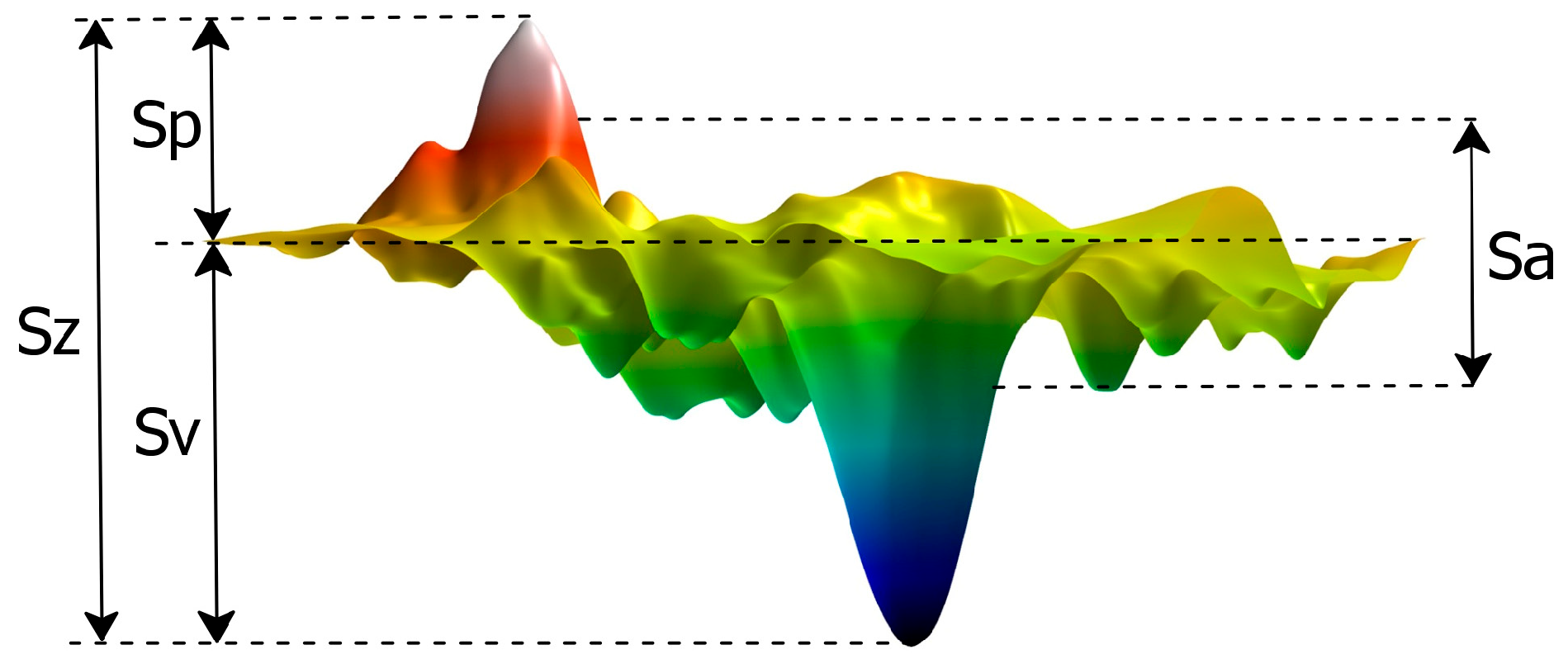
The height parameters, defined according to Standard 25178-2, are graphically shown in Figure 2.

Figure 2.
Graphical representation of height parameters.
- Arithmetical mean height, Sa, is the average of the absolute values of the heights of peaks and valleys.
- Maximum height, Sz, is the sum of the maximum height of the peak and the maximum height of the valley.
- Maximum peak height, Sp, is the largest height value of peaks on a defined area of the surface.
- Maximum valley height, Sv, is the largest depth value of valleys on a defined area of surface.
2.3.2. Functional Parameters (Stratified Surfaces) [28]
- Core height, Sk, is the distance between the highest and lowest points of the core surface.
- Reduced peak height, Spk, is the height of the protruding peaks above the core surface after the reduction process.
3. Results and Discussion
For the successful use and application of electroplating on 3D-printed components in practice, a thorough analysis of the surfaces and the resulting copper coating is essential. The effect of modifying the 3D-printed surface by tumbling (for 1 h, 2 h, or 3 h) and vaporisation was compared using height and functional surface roughness parameters. Post-processing is described in many studies in terms of roughness. In studies [29,30], only the height parameters Sa and Sz are most often monitored, which is not sufficient. Using these parameters, we can observe a decrease or increase in surface roughness; however, visual assessment reveals the creation of different surface textures. In this study, surface roughness parameters were selected that can quantify texture changes and describe specific surface properties. The results are discussed in the following paragraphs.
3.1. Surface Topography
All samples were observed using an Infinite Focus G5 microscope, and the results from three different conditions (1 to 3 h) of treatment using tumbling were compared with the results obtained after vaporisation and with the original surface. Changes in surface topography were observed and quantified using selected standardised surface roughness parameters. Multiparametric comparison allows us to evaluate even small changes between the formed surfaces. The data is presented in Table 1 and is illustrated using graphs, 3D maps, and Abbott–Firestone curves with histograms in Figure 3, Figure 4 and Figure 5.

Table 1.
Surface roughness areal parameters.
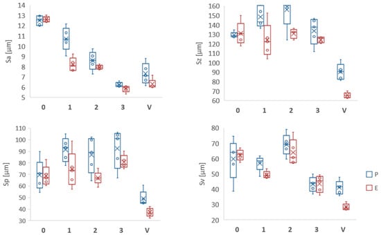
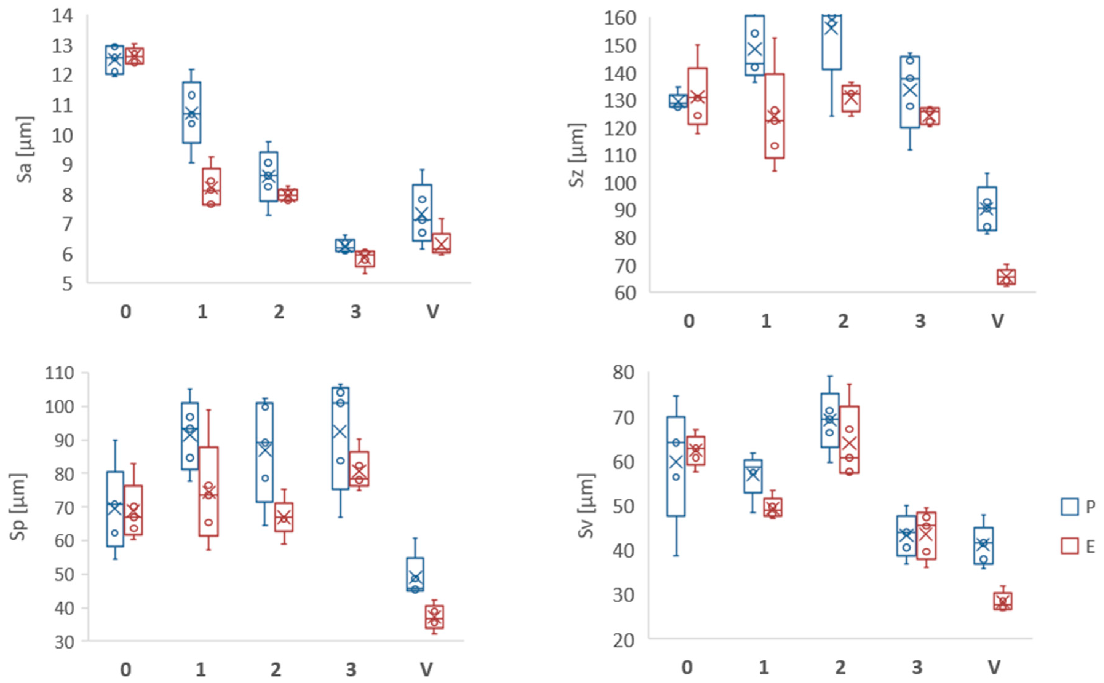
Figure 3.
Comparison of height areal roughness parameters Sa, Sz, Sp, and Sv.
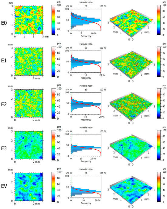
Figure 4.
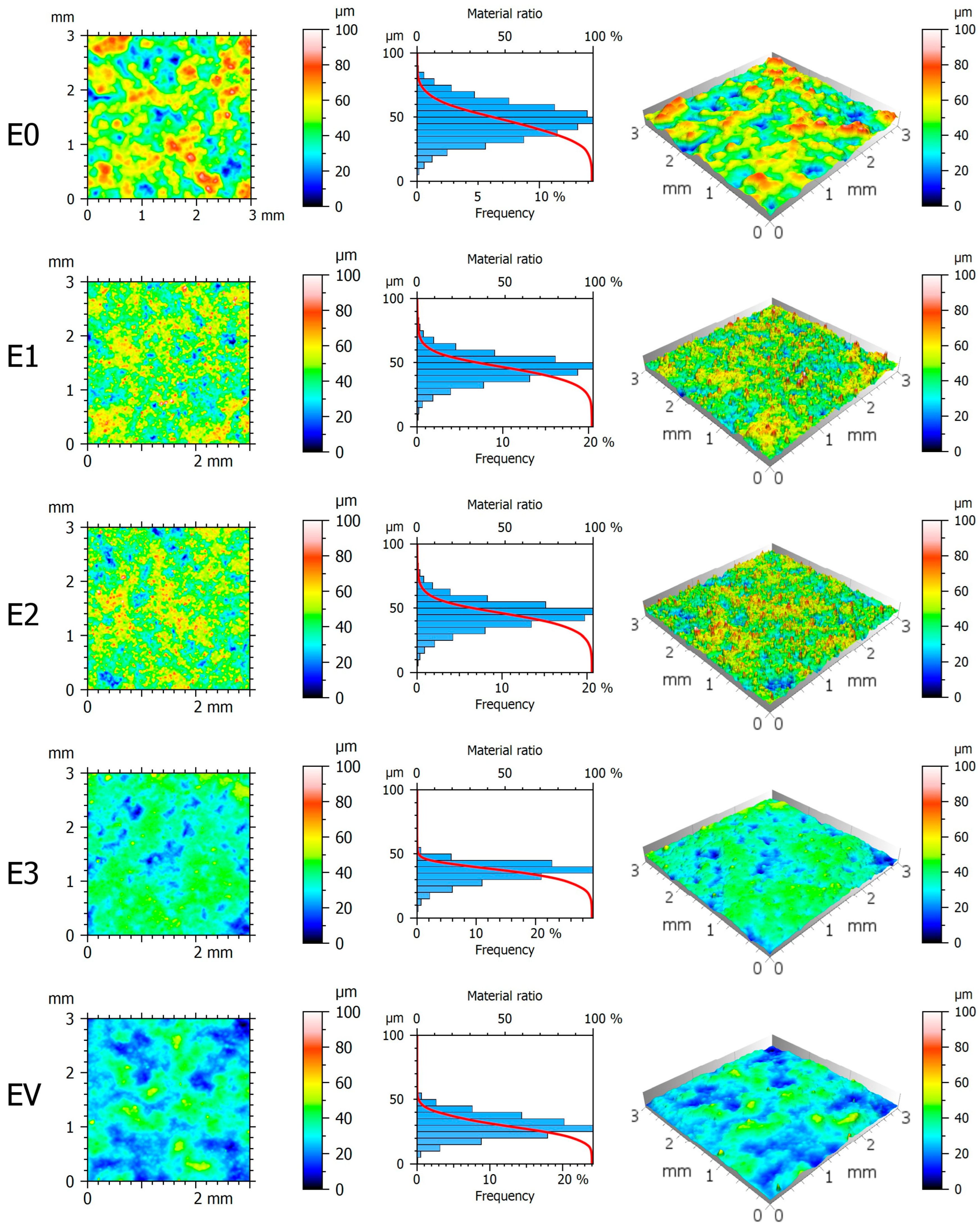
2D heat maps, 3D heat maps, and Abbott–Firestone curves with histograms of electroplating surfaces.
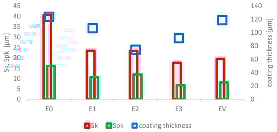
Figure 5.
Comparison of functional areal roughness parameters Sk, Spk, and coating thickness.
3.1.1. Height Parameters Sa, Sz, Sp, and Sv
Elevation parameters describe the topography of the surface. A graphical comparison of the Sa, Sz, Sp, and Sv parameters of the analysed surfaces is shown in Figure 3. These parameters provide information exclusively about elevation. The characteristics of the horizontal elements are therefore not reflected in these parameters. Each parameter exhibits different sensitivity to certain geometric aspects of the analysed surface.
The Sa parameter is the average difference in height from the median plane. It is a statistically stable parameter. It cannot detect local irregularities on the surface. For research purposes, it is necessary to monitor local changes on the surface. This can be done using the Sz parameter. This parameter consists of the Sp and Sv parameters and provides information about the maximum height value. The Sp and Sv parameters quantify whether there are higher peaks or depressions on the surface.
Figure 3 reveals that one of the main differences between the P-print (blue) and E-electroplating (red) sets in five different surface conditions (0—original, 1—tumbling 1 h, 2—tumbling 2 h, 3—tumbling 3 h, and V—vaporisation) is the size of the measured height parameters. When comparing the surfaces before and after the application of the copper coating, the Sa, Sz, Sp, and Sv parameters achieved higher values in 3D-printed samples for all surface modifications (designations 1, 2, 3, and V). Thanks to multi-parameter evaluation, we observed changes in the surface characteristics. Height parameters describe changes in surface height. To graphically illustrate these changes, height maps of the surface topography were created, which are shown in Figure 4.
The Sa value decreases significantly from State 0 to State 3, where it reaches its lowest values for P3 = 6.2 ± 0.2 µm and E3 = 5.8 ± 0.3 µm. Post-processing significantly reduces surface roughness. However, when comparing the Sa parameter values for the P and E sets (Table 1), the results showed that the largest decrease in Sa parameter values occurred in E1 (by 23.4%), where the Sa values for P1 and E1 were 10.7 ± 1.0 µm and 8.2 ± 0.6 µm, respectively.
The highest Sz values are recorded in States 1, 2, and 3, whereas State V had the lowest values. The difference between plated and unplated surfaces is particularly evident in State V, where there was a significant reduction of 27.4% in the height range after plating. Plating effectively reduces extremes in height topography, especially after prior vaporisation.
The maximum height of the protrusion Sp remains relatively high (86.9–92.4 µm) in States 1–3. Post-processing by tumbling creates protrusions (peaks) on the surface. The lowest values were achieved by the vaporised surface, where Sp was 49.2 ± 6.0 µm for set P and 37.2 ± 3.4 µm for set E. We can see that metallization suppresses the protrusions (peaks) on the surface, especially after vaporisation (by 24.7%).
Plated surfaces consistently have a lower Sv than the original printed ones, indicating the successful filling of depressions. The combination of post-processing methods and plating effectively reduces deep irregularities.
Figure 4 shows the surfaces of the E-electroplating set in five different states (0, 1, 2, 3, and V) for 2D height maps, Abbott–Firestone curves with histograms, and 3D topographic surface displays. The 2D display shows the surface texture and its height distribution. We can see the different distributions of density and the size of the elements on the surface. The colour resolution describes the height range of the examined surfaces. The characteristics of the created surfaces are represented by the Abbott–Firestone curve and histogram. The horizontal axis represents the ratio of material in percent. The origin on the 0% axis corresponds to the highest points of the surface, and 100% corresponds to the deepest points. The histogram shows the frequency distribution of the height of each point on the surface. The 3D maps provide a visualisation of the surface.
It is observed that surfaces E0, E1, and E2 achieve similar height values. The same is true for surfaces E3 and EV, which have a similar height range. The 2D maps show significantly different distributions of density and size of the surface elements. The Abbott–Firestone curves and histograms show the cumulative representations of heights and provide information about the bearing surface. The material ratio indicates improved bearing capacity and surface contact area, which is important for applications such as seals, sliding parts, or decorative layers. Samples E1 and E2 also have a similar course. The same is true for samples E3 and EV. The change is significant between E0 and E1/E2 and then between E3/EV. The histograms gradually narrow, and a difference in the smaller dispersion of heights is observed. The 3D models of surface topography visualise height differences, their distribution, and size. Samples E1 and E2 have a more pronounced texture compared to E0, E3, and EV. At the same time, E3 and EV have a smoother and more homogenised surface.
3.1.2. Functional Parameters Sk and Spk
Functional parameters Spk and Sk, based on the Abbott–Firestone curve, are used for the quantitative evaluation of surface functional properties. These parameters are particularly useful in areas where interaction between the surface and the surrounding environment is key (friction, lubrication, wear, or sealing).
Figure 5 shows a graphical comparison of the Sk and Spk parameters with the coating thickness values for individual samples (E0, E1, E2, E3, and EV). The Sk parameter had the highest value in the initial state E0 (40.6 ± 1.4 µm), whereas in the modified samples, it decreased slightly and stabilised around 19.5–23.4 µm (Table 1). The coating thickness (right axis) ranged from 74.3 to 123.7 µm. The results show that electroplating, especially at a greater layer thicknesses, effectively reduces protrusions above the functional surface area, as confirmed by the decrease in the Spk value. This effect may be desirable in applications where reduced peak roughness is required. The stability of the Sk parameter indicates that the overall load-bearing capacity of the surface was maintained.
3.2. Coating Analysis by the Destructive Method
A VHX 7000 digital microscope ( Keyence Corporation, Osaka, Japan) was used to analyse the thickness of the deposited Cu layer. After measuring the surface topography of the samples using a non-contact optical method, a destructive method was used to determine the thickness of the plated layer. Metallographic sections were prepared by cutting the sample perpendicularly and were then scanned in high resolution.
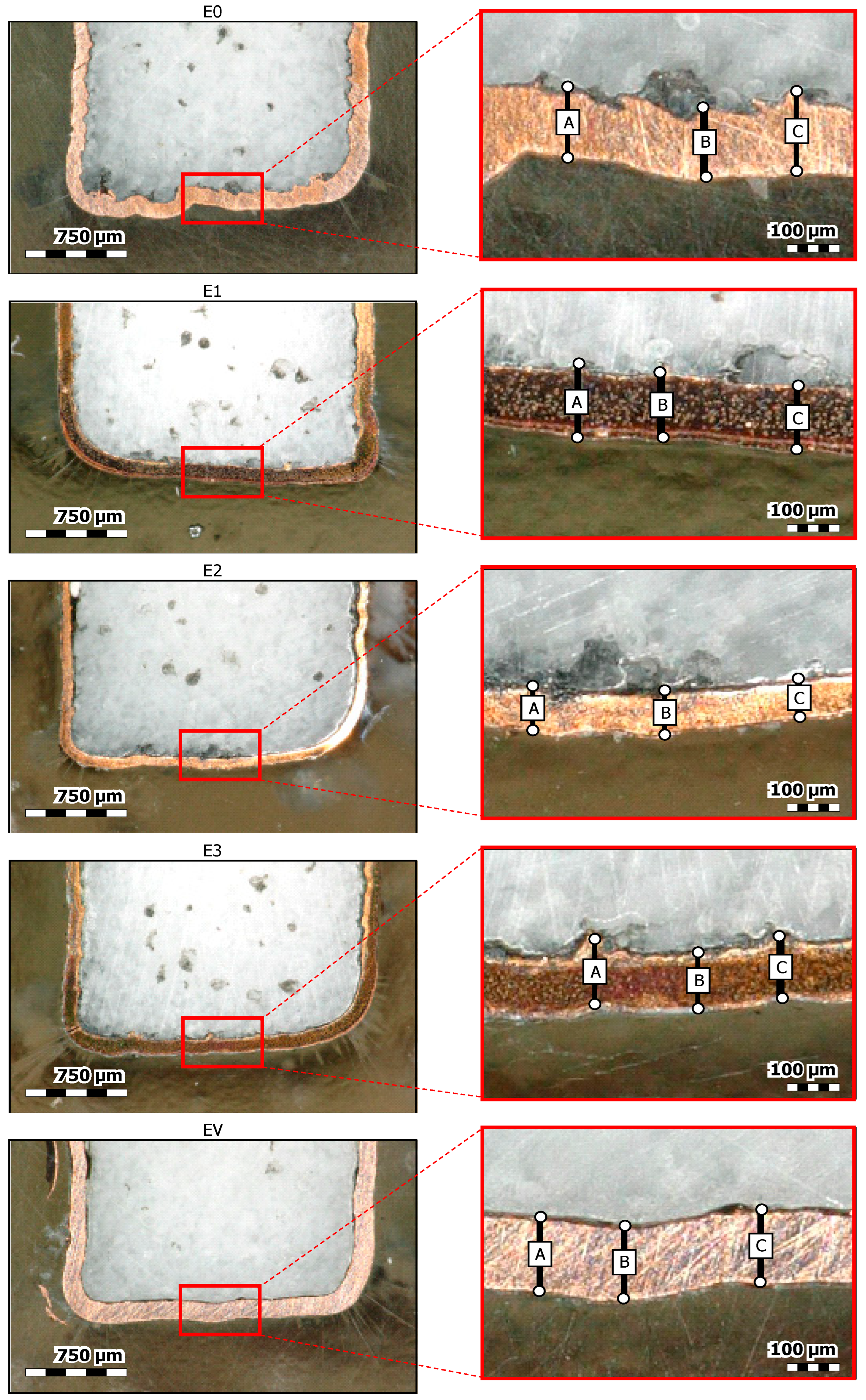
Figure 6 visualises the thickness and quality of the copper coating. The samples are labelled E0, E1, E2, E3, and EV, each with enlarged detail of the interface between the substrate and the copper layer. The enlarged detail (right) is a selected section of the sample edge, with areas A, B, and C marked, which represent the areas used for measuring the copper coating thickness. The image supports the claim that surface modification has a direct impact on the quality and thickness of the electroplated copper layer. It visually illustrates the results of the quantitative analysis described in this study. For each sample, an analysis was performed on all four sides, with five points measured on each side.
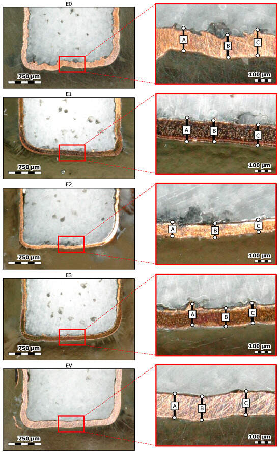
Figure 6.
Copper coating thickness measurement, A, B, and C represent the areas used for measuring the copper coating thickness.
The data obtained were then statistically evaluated and used to determine the average thickness of the plated layer. This approach allows both local and overall evaluation of the uniformity of copper deposition and identification of any deviations or defects in the layer thickness. The values are recorded in Table 2.
Table 2.
Coating thickness.
3.3. Recommendations for Further Research to Optimise This Technology
Optimisation of the plating process and the appropriate selection of surface modification techniques are essential to achieving a high-quality, uniform metal coating on 3D-printed non-conductive materials such as PA12. Surface preparation plays a critical role in determining the final surface quality. Since polymers are inherently non-conductive, it is necessary to introduce conductivity prior to electroplating.
Based on the experiments conducted, the following recommendations can be made:
- The most significant improvement in surface quality was achieved through vapor smoothing, which reduces surface roughness and seals the porosity typical of powder-based printing technologies. This step helps to minimise height variations and irregularities.
- To bridge the non-conductive nature of the polymer, a conductive interlayer film based on graphite was applied to the surface. Spray application ensures uniform coverage without losing fine surface details.
- Electrochemical copper deposition was carried out using an acidic copper electrolyte. The process parameters, including current density and plating time, were optimised to produce a uniform copper layer with a thickness of 80–130 µm, without introducing defects such as cracking or delamination.
- Microscopic observation of the surface and cross-sections was used to assess the quality of the plating, allowing for the quantification of uniformity and integrity of the metal layer. In the future, it would be appropriate to include other evaluation methods, such as the grid adhesion test, surface analysis using SEM or CLSM, or micro/nanoindentation, which will enable the quantitative correlation of surface topographic parameters with copper coating properties.
4. Conclusions
The present study analysed the influence of various methods of surface modification of 3D-printed plastic parts on the efficiency of electrochemical copper plating, especially in terms of the achieved surface quality using surface roughness parameters and the thickness of the deposited metal layer. Optimization of the surface treatment appears to be a key prerequisite for the successful electroplating of non-conductive materials, such as polyamide 12 (PA12), commonly used in selective laser sintering (SLS).
The experimental results show that surface treatment in the form of vaporisation provides the best conditions for uniform and high-quality copper coating deposition. This method significantly contributes to reducing surface roughness, improving the homogeneity and surface stratification of the resulting plated surface.
The quality of plating was verified using 3D optical profilometry and destructive microscopic analysis of sections, which confirmed the uniformity of thickness and continuity of the layer.
The findings of this study underline the importance of the controlled modification of surface topography to ensure the adhesion and efficiency of electrochemical plating. The results achieved serve as a basis for further research focused on combining multiple post-processing techniques or developing new approaches that will enable even more efficient, precise, and economically advantageous plating of 3D-printed polymer components. Overall, the data indicate that the electroplating process significantly improves surface uniformity by filling or smoothing microstructural irregularities, which leads to a reduction in peak heights and valley depths. This improvement is beneficial from both aesthetic and functional points of view for the surface, especially in tribological or sealing applications.
This research paves the way for the wider application of 3D-printed components in areas where the combination of the low weight of polymer materials with the conductivity and mechanical resistance of metal layers is required, such as in electrical engineering, the automotive industry, aerospace, and electronic device manufacturing.
Author Contributions
Conceptualization, D.K. and H.K.; methodology D.K., H.K. and J.M.; software, J.M. and F.B.; validation, D.K. and H.K.; formal analysis, D.K. and H.K.; investigation, D.K. and F.B.; resources, D.K. and F.B.; writing—original draft preparation, D.K. and H.K.; writing—review and editing, H.K. and S.R.; visualization, J.M. and F.B.; supervision, S.R. and F.B.; project administration, D.K. and S.R.; funding acquisition, D.K. and F.B. All authors have read and agreed to the published version of the manuscript.
Funding
This research was funded by the EU NextGenerationEU through the Recovery and Resilience Plan for Slovakia under Project No. 09I03-03-V04-00057. František Botko and Světlana Radchenko acknowledge projects VEGA 1/0391/22 and KEGA 017TUKE-4/2023, granted by the Ministry of Education, Research, Development, and Youth of the Slovak Republic.
Data Availability Statement
The authors declare that the data supporting the findings of this study are available within the paper.
Conflicts of Interest
The authors declare no conflicts of interest.
References
- Xiao, S.; Li, J.; Wang, Z.; Chen, Y.; Tofighi, S. Advancing Additive Manufacturing Through Machine Learning Techniques: A State-of-the-Art Review. Future Internet 2024, 16, 419. [Google Scholar] [CrossRef]
- Zhou, L.; Miller, J.; Vezza, J.; Mayster, M.; Raffay, M.; Justice, Q.; Al Tamimi, Z.; Hansotte, G.; Sunkara, L.D.; Bernat, J. Additive Manufacturing: A Comprehensive Review. Sensors 2024, 24, 2668. [Google Scholar] [CrossRef] [PubMed]
- Marsalek, P.; Sotola, M.; Rybansky, D.; Repa, V.; Halama, R.; Fusek, M.; Prokop, J. Modeling and testing of flexible structures with selected planar patterns used in biomedical applications. Materials 2021, 14, 140. [Google Scholar] [CrossRef] [PubMed]
- Prathyusha, A.L.R.; Raghu Babu, G. A review on additive manufacturing and topology optimization process for weight reduction studies in various industrial applications. Mater. Today Proc. 2022, 62, 109–117. [Google Scholar] [CrossRef]
- Mesicek, J.; Jancar, L.; Ma, Q.-P.; Hajnys, J.; Tanski, T.; Krpec, P.; Pagac, M. Comprehensive view of topological optimization scooter frame design and manufacturing. Symmetry 2021, 13, 1201. [Google Scholar] [CrossRef]
- Kozior, T. The Influence of Selected Selective Laser Sintering Technology Process Parameters on Stress Relaxation, Mass of Models, and Their Surface Texture Quality. 3D Print. Addit. Manuf. 2020, 7, 126–138. [Google Scholar] [CrossRef] [PubMed]
- Zmarzły, P.; Kozior, T.; Gogolewski, D. The effect of non-measured points on the accuracy of the surface topography assessment of elements 3D printed using selected additive technologies. Materials 2023, 16, 460. [Google Scholar] [CrossRef] [PubMed]
- Zarybnicka, L.; Petrů, J.; Krpec, P.; Pagáč, M. Effect of additives and print orientation on the properties of laser sintering-printed polyamide 12 components. Polymers 2022, 14, 1172. [Google Scholar] [CrossRef] [PubMed]
- Mesicek, J.; Vacek, M.; Ma, Q.-P.; Krejsa, M.; Hajnys, J.; Krivy, V.; Pagac, M.; Petru, J. Exploring the Impact of Saline Environments on the Properties of EOS PA2200: A Study on Weight Gain and Mechanical Characteristics. MM Sci. J. 2024, 10, 7534–7538. [Google Scholar] [CrossRef]
- Baligidad, S.M.; Kumar, G.C.; Maharudresh, A.C.; Elangovan, K. Experimental investigations on metallization in laser-sintered PA12 part using RF sputtering. Appl. Phys. A 2021, 127, 510. [Google Scholar] [CrossRef]
- Brown, S.C.; Robert, C.; Koutsos, V.; Ray, D. Methods of modifying through-thickness electrical conductivity of CFRP for use in structural health monitoring, and its effect on mechanical properties—A review. Compos. Part A Appl. Sci. Manuf. 2020, 133, 105885. [Google Scholar] [CrossRef]
- Afshar, A.; Liao, H.-T.; Chiang, F.; Korach, C.S. Time-dependent changes in mechanical properties of carbon fiber vinyl ester composites exposed to marine environments. Compos. Struct. 2016, 144, 80–85. [Google Scholar] [CrossRef]
- Macit, Ş.; Uraz, C. Electroless Cu plating on ABS plastic by using environmentally friendly chemicals. Deu Muhendis. Fak. Fen Ve Muhendis. 2018, 20, 369–375. [Google Scholar]
- Hüner, B.; Demir, N.; Kaya, M.F. Electrodeposition of NiCu bimetal on 3D printed electrodes for hydrogen evolution reactions in alkaline media. Int. J. Hydrogen Energy 2022, 47, 12136–12146. [Google Scholar] [CrossRef]
- Hopmann, C.; Fragner, J.; Haase, S. Development of electrically conductive plastic compounds based on filler combinations. J. Plast. Technol. 2014, 2, 49–67. [Google Scholar]
- Kim, M.J.; Cruz, M.A.; Ye, S.; Gray, A.L.; Smith, G.L.; Lazarus, N.; Walker, C.J.; Sigmarsson, H.H.; Wiley, B.J. One-step electrodeposition of copper on conductive 3D printed objects. Addit. Manuf. 2019, 27, 318–326. [Google Scholar] [CrossRef]
- Pollitt, J.N.; Christofidis, G.; Morrissey, J.; Birkett, J.W. Vacuum metal deposition enhancement of friction ridge detail on ballistic materials. Forensic Sci. Int. 2020, 316, 110551. [Google Scholar] [CrossRef] [PubMed]
- Juarez, T.; Schroer, A.; Schwaiger, R.; Hodge, A.M. Evaluating sputter deposited metal coatings on 3D printed polymer micro-truss structures. Mater. Des. 2018, 140, 442–450. [Google Scholar] [CrossRef]
- Islam, A.; Hansen, H.N.; Tang, P.T. Direct electroplating of plastic for advanced electrical applications. CIRP Ann. 2017, 66, 209–212. [Google Scholar] [CrossRef]
- Krupova, H.; Sternadelova, K.; Mesicek, J.; Ma, Q.-P.; Hajnys, J. Experimental evaluation of selectively laser sintered polyamide 12 surface treatment for direct electrodeposition. Prog. Org. Coat. 2024, 186, 107968. [Google Scholar] [CrossRef]
- Marciniak, D. Assessment of the surface and structure of elements produced in additive manufacturing technology after chemical treatment. MATEC Web Conf. 2021, 332, 01010. [Google Scholar] [CrossRef]
- Marciniak, D.; Szewczykowski, P.; Bielinski, M. Effect of surface modification by acetone vaporization on the structure of 3D printed acrylonitrile-butadiene-styrene elements. Polimery 2018, 63, 785–790. [Google Scholar] [CrossRef]
- Giurlani, W.; Berretti, E.; Innocenti, M.; Lavacchi, A. Measuring the Thickness of Metal Coatings: A Review of the Methods. Coatings 2020, 10, 1211. [Google Scholar] [CrossRef]
- Melentiev, R.; Yudhanto, A.; Tao, R.; Vuchkov, T.; Lubineau, G. Metallization of polymers and composites: State-of-the-art approaches. Mater. Des. 2022, 221, 110958. [Google Scholar] [CrossRef]
- Schroer, D.; Nichols, R.J.; Meyer, H. Pretreatment of polymer surfaces—The crucial step prior to metal deposition. Electrochim. Acta 1995, 40, 1487–1494. [Google Scholar] [CrossRef]
- Tischer, F.; Cholewa, S.; Düsenberg, B.; Drummer, D.; Bück, A.; Peukert, W.; Schmidt, J. Closed Loop Recycling Approach for Aged Polyamide 12 Feedstocks for Powder Bed Fusion by Precipitation from a Moderate Solvent Combined with Solvolysis. Addit. Manuf. 2025, 107, 104822. [Google Scholar] [CrossRef]
- Martynková, G.S.; Slíva, A.; Kratošová, G.; Barabaszová, K.Č.; Študentová, S.; Klusák, J.; Brožová, S.; Dokoupil, T.; Holešová, S. Polyamide 12 materials study of morpho-structural changes during laser sintering of 3D printing. Polymers 2021, 13, 810. [Google Scholar] [CrossRef] [PubMed]
- ISO 25178-2; Geometrical Product Specifications (GPS)—Surface Texture: Areal—Part 2: Terms, Definitions and Surface Texture Parameters. International Organization for Standardization: Geneva, Switzerland, 2021.
- Nagalingam, A.P.; Vohra, M.S.; Kapur, P.; Yeo, S.H. Effect of Cut-Off, Evaluation Length, and Measurement Area in Profile and Areal Surface Texture Characterization of As-Built Metal Additive Manufactured Components. Appl. Sci. 2021, 11, 5089. [Google Scholar] [CrossRef]
- Zhang, T.; Yuan, L. Understanding surface roughness on vertical surfaces of 316 L stainless steel in laser powder bed fusion additive manufacturing. Powder Technol. 2022, 411, 117957. [Google Scholar] [CrossRef]

Disclaimer/Publisher’s Note: The statements, opinions and data contained in all publications are solely those of the individual author(s) and contributor(s) and not of MDPI and/or the editor(s). MDPI and/or the editor(s) disclaim responsibility for any injury to people or property resulting from any ideas, methods, instructions or products referred to in the content. |
© 2025 by the authors. Licensee MDPI, Basel, Switzerland. This article is an open access article distributed under the terms and conditions of the Creative Commons Attribution (CC BY) license (https://creativecommons.org/licenses/by/4.0/).