Abstract
This paper proposes a lifespan extension technique for three-phase voltage inverters using hybrid offset voltage. The proposed method lengthens the inverter lifetime by independently adjusting the switching frequency of the three phases in accordance with the aging degree. To reduce the switching operation of the phase with the shortest lifetime, the proposed technique injects the offset voltage for generalized discontinuous pulse-width modulation PWM (GDPWM) into the reference voltage in the region where the switching operation of the shortest lifespan phase can be stopped. When the switching operation does not need to be stopped, the offset voltage for space vector PWM (SVPWM) is injected into the reference voltage for high inverter load current quality. An offset voltage that varies according to the need to stop the switching operation is the proposed hybrid offset voltage. Using the proposed hybrid offset voltage, the switching frequencies of the three phases are independently controllable. In addition, since only the switching operation of the phase having the shortest lifespan is reduced, the load current quality in accordance with the switching operation reduction is good compared to the conventional method to simultaneously diminish all phase switching frequencies. The proposed method significantly increases the reliability of the three-phase voltage inverter, where the thermal stress of the phase having the shortest lifespan is decreased up to 55%, whereas the inverter lifetime can be increased by 10 times. The proposed technique was verified by simulations and experiments.
1. Introduction
As a solution to rapid climate change caused by the use of fossil fuels, the dissemination of electric vehicles is increasing. Accordingly, the reliability of a three-phase inverter driving a motor of an electric vehicle is also becoming important. In particular, three-phase inverters based on SiC MOSFETs are used for high-efficiency electric vehicles [1]. SiC MOSFETs are attracting attention as highly efficient switching devices because of their small switching and conduction losses [2]. A lot of research has been conducted on the reliability of SiC MOSFETs. Typical types of degradation that SiC MOSFETs experience are chip-level degradation and package-level degradation [3]. When chip-level and package-level degradations occur, threshold voltage and on-resistance of SiC MOSFETs change [1,4].
Meanwhile, the overall converter lifetime is determined by the shortest lifespan component among the various converter components. The switching device is regarded as the shortest lifespan element among the converter components [5]. The junction temperature greatly influences the switching element lifespan [6]. Since losses raise the junction temperature, research has been conducted to extend converter life by reducing converter losses [7,8,9,10,11,12]. The method of reducing the loss of the converter to extend the lifespan is divided into a variable switching frequency method (VSFM) [7,8,9] and a method based on discontinuous PWM (DPWM) [10,11,12,13]. In the VSFM, the number of switching operations varies to reduce the converter loss. In addition, in the DPWM-based method, the total converter loss is diminished by reducing the switching loss through the clamping angle adjustment. In addition to the converter life extension method through converter loss reduction, a method using reactive power [14] and a method using switch redundancy [15] have also been proposed. One of the significant advantages of model predictive control (MPC) is its flexibility to control multiple objectives simultaneously. In the MPC methods considering the increase in converter lifetime, an additional cost function is added to reduce the number of switching transitions, along with other control objectives [16,17].
As mentioned earlier, various studies have been conducted on the aging characteristics of SiC MOSFETs, but few studies have researched the effect of aging SiC MOSFETs on the converter lifespan. In addition, a lot of methods for extending the converter lifetime have been developed, but no research has dealt with extending the lifespan reduced by aging SiC MOSFETs. Additionally, limited research considers the different aging conditions in three-phase voltage inverters. This paper proposes a technique to lengthen the lifespan of a three-phase voltage source inverter (VSI) composed of aged SiC MOSFETs using hybrid offset voltage. Moreover, a three-phase VSI lifetime prediction simulator based on the electrical characteristics of SiC MOSFET is proposed. Through the developed inverter lifetime prediction simulator, the effect of aged SiC MOSFET on the three-phase VSI lifespan was analyzed and the lifetime extension effect of the proposed technique was confirmed. The proposed method significantly increases the reliability of the three-phase voltage inverter, where the thermal stress of the phase having the shortest lifespan is decreased and the lifetime of the entire VSI is prolonged.
The structure of this paper after the introduction is as follows. Section 2 is a description of conventional carrier-based PWM. Section 3 explains the proposed lifetime extension method using hybrid offset voltage. Section 4 and Section 5 verify the proposed method using the simulations and experiments. Section 6 presents an analysis of the lifetime extension effect of the proposed technique. Section 7 compares the load current quality and losses of the proposed and conventional methods. Section 8 is the conclusion of this paper.
2. Carrier-Based PWM
A three-phase VSI is used for various purposes, such as driving a motor or connecting to a grid. Figure 1 shows a three-phase VSI composed of SiC MOSFETs. In Figure 1, Vdc and Cdc represent the inverter input voltage and DC-link capacitor, respectively. In addition, S1 to S6 mean SiC MOSFETs, which are switching devices. The three-phase motor, which is the inverter load, is expressed by the load inductor (L), the load resistor (R) and the back electromotive force (EMF). iLa denotes the a-phase load current.
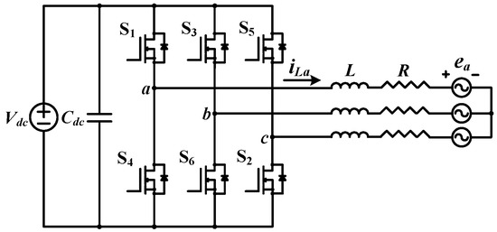
Figure 1.
Circuit diagram of three-phase VSI.
A conventional method to create a switching signal that controls a three-phase VSI, as shown in Figure 1, is to compare the carrier with a reference voltage. This method is called carrier-based PWM. Carrier-based PWM can achieve various control purposes by injecting different offset voltages into the reference voltage of each phase.
Figure 2 depicts how switching signals are generated in the carrier-based PWM. In Figure 2, vrx means the reference voltages of the x-phase (x = a, b, c). In addition, voff represents the offset voltage. Figure 2 demonstrates that the switching signals of the three-phase VSI are generated by comparing the carrier with the reference voltage plus the offset voltage. Equation (1) represents vrx_off (x = a, b, c), the x-phase reference voltage plus the offset voltage. Depending on which voltage is used as the offset voltage in Equation (1), the control technique of the inverter is different.
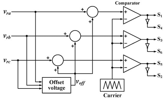
Figure 2.
Carrier-based PWM.
2.1. Space Vector PWM
Space vector PWM (SVPWM) is a method to control three-phase VSIs because of its excellent load current quality and high maximum modulation. SVPWM is implemented by applying the following voltage as an offset voltage Equation (2) [18].
In Equation (2), voff_sv means the offset voltage for SVPWM. In addition, vrmax and vrmin denote the maximum and minimum among vra, vrb and vrc, respectively. Figure 3 shows vra, voff_sv and vra_sv, which is the sum of vra and voff_sv when SVPWM is applied.
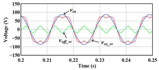
Figure 3.
vra, voff_sv, and vra_sv when SVPWM is applied.
2.2. Generalized Discontinuous PWM
DPWM is characterized in that switching loss can be reduced because the switching operation is stopped in a specific period. When a three-phase VSI is controlled by DPWM, the switching operation is stopped by 120° per phase. Among various DPWM techniques, the generalized DPWM (GDPWM) can effectively decrease the inverter switching loss because the switching operation is stopped when the absolute load current is the largest. GDPWM is implemented by applying an offset voltage calculated by Equation (3) [19].
In Equation (3), voff_d means the offset voltage to implement GDPWM. In addition, imax represents the load current in the phase with the largest reference voltage. Conversely, imin is the load current in the phase with the smallest reference voltage. Figure 4 shows iLa, vra, voff_d and vra_d, the sum of vra and voff_d when GDPWM is applied. The switching operation can be stopped by setting vra_d to Vdc/2 or −Vdc/2 when the absolute load current is the largest using voff_d. This operation can reduce switching loss.
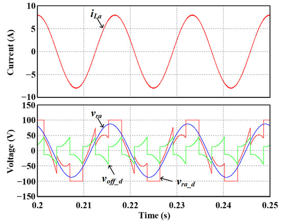
Figure 4.
iLa, vra, voff_d, and vra_d when GDPWM is applied.
The proposed method independently regulates the switching frequencies of all phases in the three-phase VSI using the hybrid offset voltage, a mixture offset voltage of SVPWM and GDPWM. This hybrid offset voltage effectively extends the inverter lifespan while mitigating load current quality deterioration.
3. Proposed Inverter Lifetime Extension Method Using Hybrid Offset Voltage
The three-phase inverter consists of 6 switching devices, as shown in Figure 1. Switching devices show different aging degrees under the same aging conditions [1,4]. Therefore, switching devices constituting one inverter have different aging rates under the same operating conditions. Since the inverter lifespan is decided by the most aged switching device, in this paper, the inverter lifespan is extended by regulating only the switching operation of the phase with the shortest lifetime.
Several techniques for monitoring the aging of switches have been proposed [20,21,22]. In [20], the on-resistance of the switching device was used for the aging monitoring. In addition, turn-on time or drain-source voltage was used to estimate the switching device aging [21,22]. Since the aging monitoring method of the switching device is out of the scope of this paper, a detailed description is not covered.
3.1. Hybrid Offset Voltage
The region where the switching operation is stopped in the DPWM is called the clamping region. There are studies that regulate the switching frequencies of all phases by changing the width of the clamping region of DPWM and that extend the converter lifespan [10,11,12]. In these studies, the width of all phase clamping regions of the converter was varied equally. However, these methods regulate the switching frequencies of all phases equally without considering the aging of each phase, further deteriorating the load current quality. Since the overall converter lifetime is determined by the shortest lifespan phase, reducing only the switching frequency of the most aged phase can extend the overall converter lifetime. Therefore, the proposed scheme only stops the switching operation of the phase having the shortest lifetime in the clamping region, thereby increasing the overall lifespan of the converter and mitigating the degradation of the converter output quality.
In the proposed technique, individual phase switching frequency control is achieved using the hybrid offset voltage, the mixed offset voltage of SVPWM and GDPWM expressed in Equations (2) and (3). In the phase where the switching frequency needs to be reduced, voff_d is used in the clamping region suitable for that phase and voff_sv is used in the remaining region, called the non-clamping region, to obtain high-quality load current. The load current quality of SVPWM is better than sinusoidal PWM (SPWM), which controls the inverter with zero offset voltage [23]. Therefore, the inverter is controlled by SVPWM in the non-clamping region. Equation (4) represents the proposed hybrid offset voltage. In Equation (4), voff_hy means the proposed hybrid offset voltage.
Figure 5 shows the results when a three-phase inverter is controlled by the proposed hybrid offset voltage. In Figure 5, assuming that the most aged phase is a-phase, clamping operation is performed during the one-third period of a-phase. Figure 5 indicates that voff_d is injected into the reference voltage to stop the a-phase switching operation when the largest load current flows in the a-phase. In addition, voff_sv is injected in the remaining region.
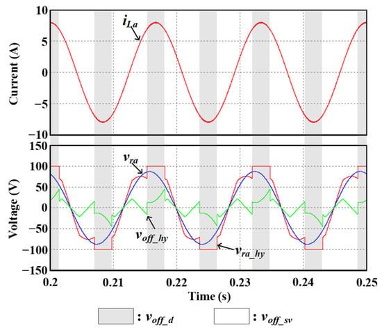
Figure 5.
iLa, vra, voff_sv, and vra_hy when the proposed hybrid offset voltage is applied.
Equation (5) represents the reference voltages plus the hybrid offset voltage. These reference voltages are compared with the carriers to generate a switching signal for the inverter control. In Equation (5), vrx_hy is the reference voltage of x-phase (x = a, b, c) plus the hybrid offset voltage.
3.2. Determination of Clamping Region
The switching operation is stopped in the specific region by the proposed technique. The load currents determine the region to stop the switching operation.
Figure 6 shows how to determine the clamping region of a-phase. In Figure 6, θa means the clamping angle of a-phase. The clamping angle determines the width of the clamping region. The range of θa is 0° to 60°. This is because the switching operation can be halted for one-third of the period per phase. In Figure 6, UCau, UCal, LCau and LCal are the upper limit for upper clamping in a-phase, the lower limit for upper clamping in a-phase, the upper limit for lower clamping in a-phase and the lower limit for lower clamping in a-phase, respectively.
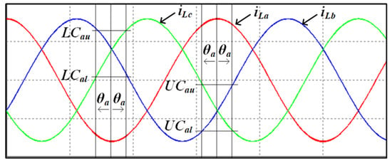
Figure 6.
Determination of clamping region in a-phase.
Figure 6 shows that the a-phase upper clamping region is when iLb and iLc are between UCau and UCal. Moreover, the a-phase lower clamping region is when iLb and iLc are between LCau and LCal. In other words, the clamping region can be determined using the two-phase load currents.
Equation (6) shows how to calculate UCxu, UCxl, LCxu and LCxl (x = a, b, c). In Equation (6), iLpeak means the peak load current. Furthermore, θb and θc denote the clamping angle of the b-phase and c-phase, respectively.
Moreover, Table 1 summarizes the conditions for determining the clamping regions of all phases.

Table 1.
Condition for clamping region determination.
Figure 7 is a flow chart showing the method of determining the proposed hybrid offset voltage. Figure 7 demonstrates that the proposed hybrid offset voltage is calculated through the two-phase load current, UCxu, UCxl, LCxu and LCxl (x = a, b, c).
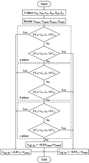
Figure 7.
Flow chart for determination of proposed hybrid offset voltage.
Figure 8 represents the control block of the inverter lifetime extension method based on the proposed hybrid offset voltage. In Figure 8, irLd and irLq mean the references of the d- and q-axis load currents, respectively. Moreover, iLd and iLq indicate the d- and q-axis load currents, respectively. θri is the reference angle of the load current. By regulating the clamping angles of the three phases, the proposed method can control the switching frequencies of the three phases. By preferentially reducing the switching frequency of the phase with the shortest lifespan, it is possible to effectively lengthen the inverter lifespan and mitigate the deterioration of the inverter load current quality caused by the switching frequency reduction. Furthermore, the lifespan of the inverter can be further extended by appropriately adjusting all phase switching frequencies, not just the most aged phase.
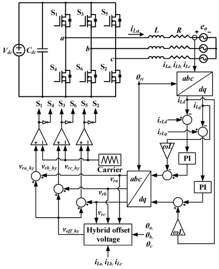
Figure 8.
Control block of proposed inverter lifetime extension method using hybrid offset voltage.
4. Simulation Results
This section verifies the proposed method through the simulation. Table 2 summarizes the simulation parameters. A three-phase R-L load was used as the inverter load in the simulation.

Table 2.
Simulation parameters used in this paper.
The simulation results obtained from the proposed inverter lifetime extension method using hybrid offset voltage according to clamping angles are depicted in Figure 9. Figure 9 represents iLa, iLb, iLc and switching signals of S1, S3 and S5. Figure 9a is in θa = θb = θc = 0°. Furthermore, Figure 9b is in θa = 30° and θb = θc = 0°. Moreover, Figure 9c is in θa = 60° and θb = θc = 0°. Figure 9a–c indicates that the a-phase switching operation can be stopped without halting the b- and c-phase switching operations. In addition, as θa increases, the region where the a-phase switching operation stops increases. Meanwhile, Figure 9d represents the simulation results when θa, θb and θc are set to 60°, 15° and 45°, respectively. Figure 9d demonstrates that the clamping regions of each phase can be controlled by setting the clamping angle of each phase differently.
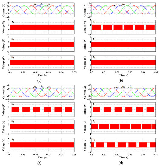
Figure 9.
Simulation results of iLa, iLb, iLc, and switching signals of S1, S3, and S5 obtained from the proposed method according to clamping angles (a) θa = θb = θc = 0° (b) θa = 30°, θb = θc = 0° (c) θa = 60°, θb = θc = 0° (d) θa = 60°, θb = 15°, θc = 45°.
The simulation results of the three-phase load current, three-phase reference voltage plus offset voltage and offset voltage obtained from the proposed method according to clamping angles are represented in Figure 10. Figure 10a is the result when the three-phase clamping angles are 0°. Since the three-phase clamping angles are 0°, it operates as SVPWM in all regions. On the other hand, Figure 10b is the result in the case of θa = 30° and θb = θc = 0°. Additionally, Figure 10c is obtained under the condition of θa = 60° and θb = θc = 0°. Figure 10b,c demonstrates that as θa increases, the range operating as GDPWM increases. Figure 10d is when all three phase clamping angles are set differently. Figure 10d demonstrates that the region operating as GDPWM changes according to the clamping angle of each phase.
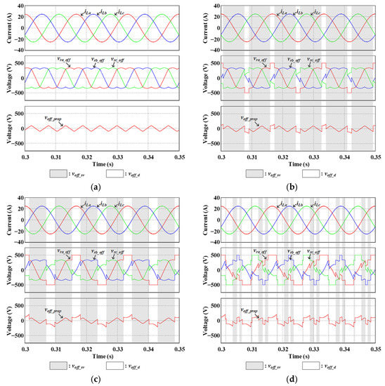
Figure 10.
Simulation results of the three-phase load current, three-phase reference voltage plus offset voltage, and offset voltage obtained from the proposed method according to clamping angles (a) θa = θb = θc = 0° (b) θa = 30°, θb = θc = 0° (c) θa = 60°, θb = θc = 0° (d) θa = 60°, θb = 15°, θc = 45°.
Figure 11 shows the switching frequencies of three phases when θa changes while θb and θc are maintained at 0°. The results in Figure 11 were obtained from the simulation. Figure 11 indicates that the b- and c-phase switching frequencies do not change and only the a-phase switching frequency can be controlled independently. In addition, the desired switching frequency can be obtained by regulating the clamping angle.
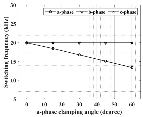
Figure 11.
Switching frequencies of three phases according to a-phase clamping angle variation in θb = θc = 0° (obtained from simulation).
5. Experimental Results
This section confirms the performance of the proposed inverter lifespan extension technique through experiments. The parameters used in the experiment are the same values in Table 2. In addition, the three-phase R-L load was used as the inverter load in the experiment. Moreover, the digital signal processor used to control the three-phase VSI is TMS320F28335 (Texas Instruments, Dallas, TX, USA). The three-phase inverter consists of SiC MOSFETs (SCT3080AL, Rohm Semiconductor, Kyoto, Japan). The gate driver used is the SKHI22BR. Figure 12 represents the experimental setup used in this paper.
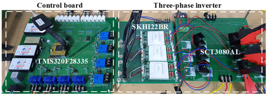
Figure 12.
Experimental setup.
The experimental results of iLa and switching signals of S1, S3 and S5 obtained from the proposed method according to clamping angles are represented in Figure 13. Figure 13 implies that the proposed technique can independently control the three-phase clamping regions. In Figure 13a, all three phase clamping angles are set to 0°, in which the inverter is operated as the SVPWM. In Figure 13b, all three phase clamping angles are set to 60°, in which the inverter is operated as the GDPWM. Figure 13a,c,d represents that the proposed method can control the a-phase clamping region while the b- and c-phases are in the continuous switching operation. Moreover, Figure 13e demonstrates that the proposed technique can regulate the width of the three-phase clamping regions differently.
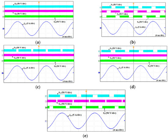
Figure 13.
Experimental results of iLa and switching signals of S1, S3 and S5 obtained from the proposed method according to clamping angles (a) θa = θb = θc = 0° (SVPWM) (b) θa = θb = θc = 60° (GDPWM) (c) θa = 30°, θb = θc = 0° (d) θa = 60°, θb = θc = 0° (e) θa = 60°, θb = 15°, θc = 45°.
Figure 14 shows the experimental results of iLa, iLb, iLc and the switching signal of S1 obtained from the proposed method according to clamping angles. Figure 14 represents that the three-phase load current is well controlled as a sinusoidal waveform under the reduction in the a-phase switching operation.
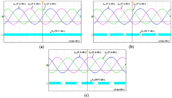
Figure 14.
Experimental results of iLa, iLb, iLc, and switching signal of S1 obtained from the proposed method according to clamping angles (a) θa = θb = θc = 0° (SVPWM) (b) θa = 30°, θb = θc = 0° (c) θa = 60°, θb = θc = 0°.
Figure 15 represents the experimental results of the a-phase load current, switching signal of S1 and vra_hy obtained from the proposed method according to clamping angles. Figure 15 indicates that the regions operating with SVPWM and GDPWM differ according to the clamping angle. In Figure 15a, where the clamping angle of all phases is 0°, the inverter operates as SVPWM in all regions. However, in Figure 15b, where the clamping angle of all phases is 60°, the inverter operates as GDPWM in all regions. On the other hand, in Figure 15c,d, the a-phase clamping angles are 30° and 60°, respectively. Therefore, the region operating with GDPWM is larger in Figure 15d than in Figure 15c. In the clamping region, vra_hy is fixed at Vdc/2 or −Vdc/2 to halt the switching operation.
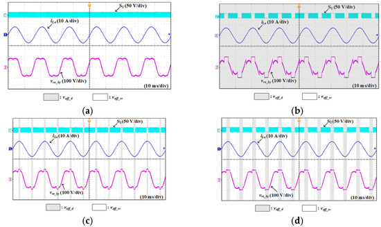
Figure 15.
Experimental results of iLa, switching signal of S1, and vra_hy obtained from the proposed method according to clamping angles (a) θa = θb = θc = 0° (SVPWM) (b) θa = θb = θc = 60° (GDPWM) (c) θa = 30°, θb = θc = 0° (d) θa = 60°, θb = θc = 0°.
Figure 16 represents the experimental results of iLa, switching signal of S1 and voff_hy obtained from the proposed method according to clamping angles. Similar to Figure 15, Figure 16 demonstrates that the regions operating with SVPWM and GDPWM differ according to the clamping angle. In Figure 16a, where the clamping angles of all phases are 0°, voff_hy is the same as the offset voltage for SVPWM. In addition, in Figure 16b, where the clamping angles of all phases are 60°, voff_hy is the same as the offset voltage for GDPWM. Meanwhile, in Figure 16c,d, the offset voltage for GDPWM is used in the clamping region of a-phase and the offset voltage for SVPWM is used in the non-clamping region.
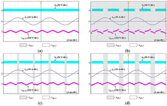
Figure 16.
Experimental results of iLa, switching signal of S1, and voff_hy obtained from the proposed method according to clamping angles (a) θa = θb = θc = 0° (SVPWM) (b) θa = θb = θc = 60° (GDPWM) (c) θa = 30°, θb = θc = 0° (d) θa = 60°, θb = θc = 0°.
Figure 17 shows the switching frequencies of each phase when the a-phase clamping angle changes while the b- and c-phase clamping angles are set to 0°. The results in Figure 17 were obtained from the experiment. Similar to the previous simulation results, it can be confirmed in the experiment that only the switching frequency of the a-phase can be diminished independently while maintaining the b-phase and c-phase switching frequencies. Therefore, Figure 11 and Figure 17 indicate that the switching frequency of the phase having the shortest lifespan can be diminished without affecting the switching frequency of other phases by using the proposed hybrid offset voltage.
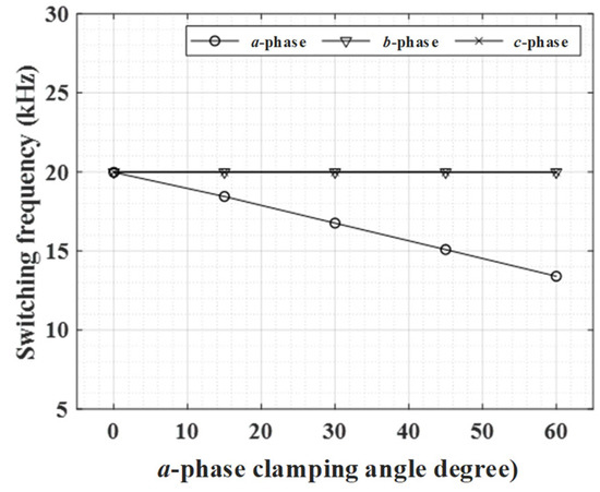
Figure 17.
Switching frequencies of each phase according to a-phase clamping angle in θb = θc = 0° (obtained from the experiment).
In this section, the ability to regulate each phase switching frequency of the proposed method was verified by experiments. Experiment results demonstrate that the switching frequency can be independently controlled according to the clamping angle of each phase as in the simulation and that the proposed hybrid offset voltage is calculated as the offset voltage for SVPWM or GDPWM according to the clamping region.
6. Analysis of Lifetime Extension Effect of Proposed Technique
This section verifies the effect of the proposed lifetime extension technique. To do this, it is analyzed how the lifespan of the inverter changes when the switch ages. As mentioned earlier, the lifespan of an inverter is the same as the lifespan of elements with the shortest lifespan. The switching device lifetime is judged to be the shortest [5], so in this paper, the inverter lifetime is estimated from the switching device lifetime. The lifetime of a SiC MOSFET is expressed as Equation (7) [6,24]. It should be noted that
In Equation (7), Nf denotes the number of cycles where the switching device fails. Additionally, db, Vc, iB and ton represent bond wire diameter, voltage rating, current per bond and heating time, respectively. Moreover, Tj is the junction temperature. In addition, ΔTj and Tjmin denote the junction temperature variation and the minimum of the junction temperature in Kelvin degrees, respectively. Without information on iB and db, it can be assumed to be 10 A and 400 μm, respectively [25]. Vc is a value obtained by dividing the rated voltage of the switching device by 100. Since the rated voltage of the SiC MOSFET used in this paper is 650 V, Vc becomes 6.5. ton depends on the mission profile. Since the duty of the mission profile used in this paper is 0.5 and the frequency is 0.3 Hz, ton is 1.66 s. Table 3 summarizes the parameters of Equation (7) used in this paper.

Table 3.
Parameter in Equation (7).
As shown in Equation (7), Nf can be calculated only when Tj is known. In this paper, Tj is estimated by the Foster thermal model and losses of SiC MOSFET. The lifetime of the SiC MOSFET and the inverter is calculated through the junction temperature.
6.1. Foster Thermal Model
The Foster thermal model of SCT3080AL is expressed in Figure 18 and Table 4. In Figure 18, Ptr is the total loss of the transistor. The case temperature is represented by Tc. In this paper, Tc is assumed to be 50 °C.

Figure 18.
Foster thermal model.

Table 4.
Parameter in Foster thermal model of SCT3080AL.
6.2. Loss of Fresh and Aging SiC Mosfet
To calculate Tj using the Foster thermal model in Figure 18, the transistor losses must be known. To this end, the electrical characteristics of fresh and aged SiC MOSFETs were measured through a double pulse test. Aged SiC MOSFET was obtained by accelerated aging stress with a high electric field. The SiC MOSFET used for characteristic measurement is SCT3080AL.
Figure 19 compares electrical characteristics between fresh and aged SiC MOSFETs. In Figure 19, Vds, Ids, Eon, Eoff, VF, IF and Err are drain-source voltage, drain-source current, transistor turn-on energy, transistor turn-off energy, forward diode voltage, diode current and diode reverse recovery current, respectively. Figure 19 indicates that as the SiC MOSFET, SCT3080AL, ages, all electrical characteristics increase except turn-off energy. In addition, the turn-off energy is slightly reduced compared to before aging. Using the switching characteristics of Figure 19, the loss of the switching device was calculated using PSIM. Losses were calculated in Table 5.
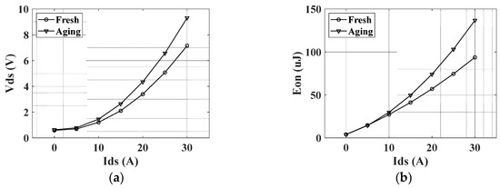
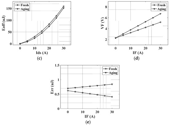
Figure 19.
Comparison of electrical characteristics between fresh and aged SiC MOSFETs (a) Vds versus Ids curve (b) Eon versus Ids curve (c) Eoff versus Ids curve (d) VF versus IF curve (e) Err versus IF curve.

Table 5.
Parameter used in loss calculation.
Figure 20 shows loss distributions of switching devices (S1, S3, S5, S4, S6, S2) according to clamping angle when a-phase switches in the inverter are aged. In Figure 20, PTcon, PTsw, PDcon and PDsw mean transistor conduction loss, transistor switching loss, diode conduction loss and diode switching loss, respectively. It should be noted that PDsw, known as reverse recovery loss, appears when the diode changes from the forward conduction phase to the reverse conduction phase. For SiC MOSFET, the reverse recovery loss is negligible. To calculate the loss of a-phase switches, the electrical characteristics of the aged SiC MOSFET in Figure 19 were used. In addition, to calculate the loss of b-phase and c-phase switches, the electrical characteristics of the fresh SiC MOSFET in Figure 19 were used.
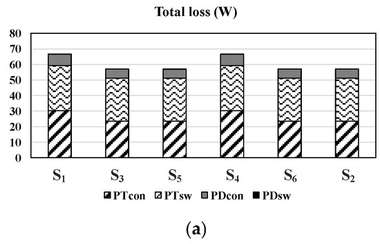
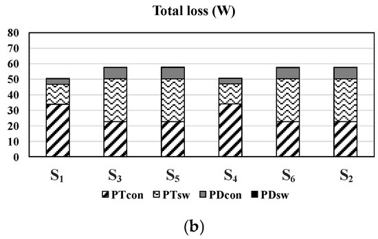
Figure 20.
Loss distributions of switching devices (S1, S3, S5, S4, S6, S2) according to clamping angle when a-phase switches in the inverter are aged (a) θa = θb = θc = 0° (b) θa = 60°, θb = θc = 0°.
Figure 20a shows loss distributions when all clamping angles are 0°. As shown in Figure 20a, due to the aged a-phase switches, all four types of losses of the a-phase devices, S1 and S4, are larger than the b-phase and c-phase devices. However, in Figure 20b, the loss distribution when the a-phase clamping angle is set to 60°, demonstrates that the loss of S1 and S4 is diminished by the proposed method. Therefore, Figure 20 confirms that the proposed technique can decrease the loss of the switching devices having the shortest lifetime.
6.3. Lifetime Estimation Using Junction Temperature
As mentioned earlier, the junction temperature is required for calculating the inverter lifetime. The Foster thermal model and the losses of the switching device are used to calculate Tj. In this subsection, using the simulation, the inverter lifetime is estimated by calculating Tj when the a-phase of the three-phase inverter is aged. Moreover, the expected lifetime extension of the inverter when applying the proposed technique is examined.
For inverter lifetime estimation, a mission profile was used to change the output power from 14 kW to 8 kW. The period of the mission profile used was 3.33 s. It operates at 14 kW for 1.67 s and 8 kW for the remaining 1.67 s. The switching device lifetime becomes shorter as the change in Tj rises. Therefore, to effectively reduce the change in the junction temperature, the proposed method was applied when the output was 14 kW. In addition, SVPWM was applied when the output was 8 kW.
Figure 21 shows transistor junction temperatures according to clamping angle when a-phase switches are aged and other-phase switches are fresh. In Figure 21, Tj(Ty) is the transistor junction temperature of Sy (y = 1, 2, 3, 4, 5, 6). Figure 21a represents transistor junction temperatures in θa = θb = θc = 0°. Moreover, Figure 21b shows the transistor junction temperature in θa = 60° and θb = θc = 0°. Figure 21a indicates that ΔTj and Tjmin of a-phase switches are larger than those of other phase switches. This is because, as shown in Figure 20a, the losses of S1 and S4 are greater than that of the other fresh phase switches. ΔTj of S1, which is the a-phase upper switch, is 24.8 °C and ΔTj of S3 is 19.8 °C. However, Figure 21b demonstrates that thanks to the decrease in the a-phase switching operation by the proposed technique, the variation of Tj(T1), denoted by ΔTj(T1), is reduced to 13.7 °C. Furthermore, since the other phases do not reduce the switching frequency, there is little change in junction temperature.
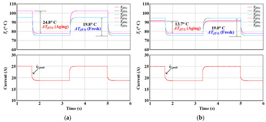
Figure 21.
Transistor junction temperatures according to clamping angle when a-phase switches are aged, and other phase switches are fresh (a) θa = θb = θc = 0° (b) θa = 60°, θb = θc = 0°.
Figure 22 shows ΔTj of each switch when the a-phase clamping angle changes while the b- and c-phase clamping angles are set to 0° in a three-phase inverter with aged a-phase. Figure 22 shows that as the clamping angle of the a-phase increases, the junction temperature fluctuation of the a-phase switch decreases. In addition, it can be seen that the switches of the remaining phases hardly change.
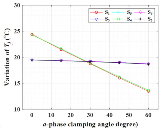
Figure 22.
ΔTj of S1, S3, S5, S4, S6, and S2 according to clamping angle when θb = θc = 0°.
Equation (7) expresses the lifetime of the switch as the number of cycles. To express this as time, the following Equation (8) is used.
In Equation (8), Lsw represents the switching device lifetime. Tprofile means the period of the mission profile. The Tprofile used in this paper is 3.33 s. The lifetime of each switch can be estimated using Equations (7) and (8), Table 3 and Figure 22. Figure 23 shows the lifetime of all switches and three-phase inverter according to the a-phase clamping angle. The result in Figure 23 is obtained when the a-phase switches of the three-phase inverter are aged and other phase switches are fresh.
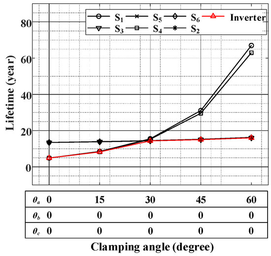
Figure 23.
Lifetimes of all switches and three-phase inverter according to the a-phase clamping angle variation.
In Figure 23, the red line represents the three-phase inverter lifetime. The lifespan of the three-phase inverter is determined to be the shortest lifetime among the six switching devices constituting the three-phase inverter. When the a-phase clamping angle is 0°, the lifetimes of the a-phase switches are about 5 years, shorter than the rest of the switches (about 13 years). However, as the a-phase clamping angle increases, the a-phase switch lifetime rises. Eventually, when the clamping angle reaches 30°, the lifetimes of all switches become similar. If the a-clamping angle is raised from 30°, the lifespan of the a-phase switch increases, but since the overall inverter lifespan is decided by the switching device having the shortest lifespan, the overall inverter lifespan does not show a significant increase after the a-phase clamping angle is 30°.
Figure 24 shows all switches and three-phase inverter lifetimes according to the three-phase clamping angle variation. Unlike Figure 23, in Figure 24, the b- and c-phase clamping angles are set to extend the inverter lifetime even when the a-phase clamping angle is over 30°. As a result, the inverter lifetime increases even when the a-phase clamping angle is more than 30°. Since the proposed technique can independently control the three-phase switching frequencies, the inverter lifetime can be greatly increased by properly setting the three-phase clamping angles, as shown in Figure 24.
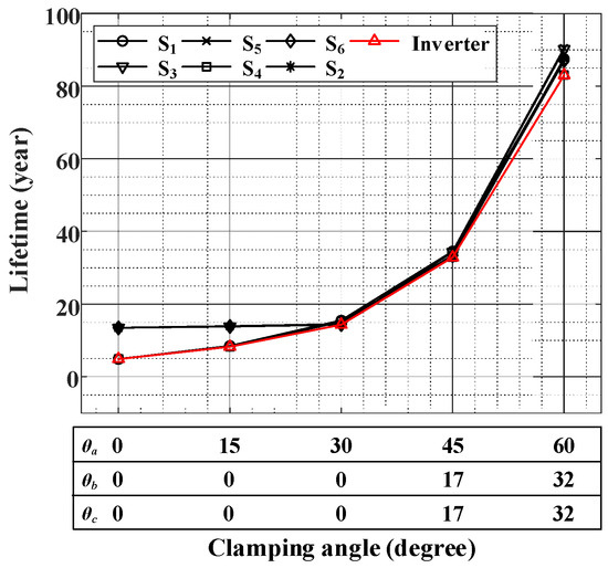
Figure 24.
Lifetimes of all switches and three-phase inverter according to the three-phase clamping angle variation.
7. Comparison of Loss and Load Current Quality between Conventional and Proposed Techniques
In this section, the loss and load current quality of the conventional and the proposed techniques are compared. Conventional converter lifetime extension methods are classified into VSFMs [7,8,9] and DPWM-based techniques [10,11,12]. The VSFM extends the converter lifespan by changing the converter switching frequency. In addition, the DPWM-based technique extends the converter lifespan by changing the width of the clamping region. That is, in the existing techniques, the converter switching frequencies of all phases are equally lowered to extend the converter’s lifetime. However, only the switching frequency of the phase having the shortest lifespan can decrease by the proposed method.
There are two major differences between the existing DPWM-based and proposed techniques. The first difference is that the conventional DPWM-based technique adjusts the width of the clamping region of all phases to the same value. However, the proposed technique can adjust the clamping region of each phase differently. This feature improves the load current quality by optimally setting the region where the switching operation stops. The second difference is that the existing DPWM-based technique does not inject offset voltage in the non-clamping region. That is, it is operated with SPWM. However, the proposed technique injects the offset voltage for SVPWM to improve the load current quality in the non-clamping region.
The SVPWM-based VSFM and the DPWM-based lifetime extension technique are used for performance comparison with the proposed technique. The VSFM decreases the switching frequency driven by SVPWM to extend the inverter’s lifetime. In addition, the DPWM-based technique extends the inverter lifetime by adjusting the width of the clamping region of all phases to be the same. The loss and load current total harmonic distortion (THD) of the above two existing techniques and the proposed technique are compared through simulation under the condition of Table 5. In addition, the inverter used for the simulation consists of aged SiC MOSFETs in a-phase and fresh SiC MOSFETs in other phases.
Figure 25 shows the loss comparison between existing techniques (SVPWM, DPWM) and the proposed technique in accordance with the switching frequency reduction in the a-phase. Figure 25a represents the loss of S1 which is an aged a-phase upper switch. Figure 25b shows the loss of S4 which is an aged a-phase lower switch. The loss in Figure 25 is the sum of both the transistor and the diode losses. The SVPWM-based VSFM decreases the a-phase switching frequency by reducing all phase switching frequencies of the inverter. In the DPWM-based lifetime extension technique, the a-phase switching operations are diminished by equally reducing the width of the clamping region of all phases. In other words, existing techniques must lower all phase switching frequencies for extending the aged phase lifetime. However, the proposed method can decrease the switching frequency of the aged phase selectively by shortening only the width of the aged phase clamping region thanks to the hybrid offset voltage. Figure 25 shows that all three techniques reduce the loss of a-phase switches by decreasing the switching frequency. In addition, Figure 25 demonstrates that the proposed method can reduce the loss more than the existing methods under the same switching frequency reduction condition. In particular, the reason why the loss of the SVPWM-based technique is greater than that of the existing DPWM-based method and the proposed method at the same switching frequency is that the switching loss can be effectively diminished in the DPWM-based and proposed methods by stopping the switching operation when the current is the largest.
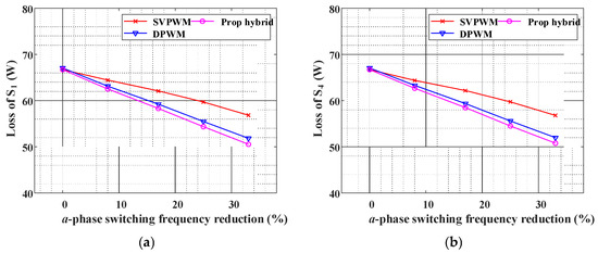
Figure 25.
Comparison of loss between existing techniques (SVPWM, DPWM) and the proposed technique in accordance with a-phase switching frequency reduction (a) loss of S1 (b) loss of S4.
On the other hand, the effect of extending the switch lifespan increases as the loss decreases. Therefore, the proposed technique has a greater effect of prolonging the lifespan of the switch than the existing techniques in the same switching operation reduction.
Figure 26 compares the THD of load current between the proposed and the existing methods in accordance with the a-phase switching operation decrease. Figure 25 demonstrates that the existing techniques reduce all phase switching frequencies for lengthening the a-phase lifetime, while the proposed technique only diminishes the switching operation of the aged phase. Figure 26a shows THDs of iLa, iLb and iLc obtained from the three techniques in accordance with the a-phase switching operation decrease. Figure 26a shows that the three-phase load current THD obtained from the proposed technique is smaller than that of the existing methods. In particular, comparing the THD of iLa in the existing DPWM-based technique and the proposed technique indicates that the THD of iLa in the proposed technique is small than that in the existing DPWM-based method. This is because, in the conventional DPWM-based technique, the offset voltage is not injected in the non-clamping region, so the inverter operates by SPWM. However, in the proposed technique, the inverter operates by SVPWM in the non-clamping region. Therefore, the proposed technique has better load current quality than the existing DPWM-based technique even when the width of the clamping region is equally changed. Since the switching operations in the b- and c-phases are not reduced in the proposed method, the load current THD is small than that of the existing methods.
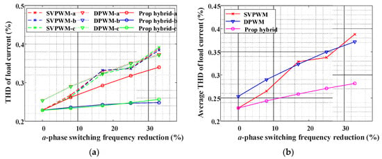
Figure 26.
Comparison of load current THD of the proposed method and the existing methods (SVPWM, DPWM) in accordance with a-phase switching frequency decrease (a) three-phase load current THD (b) average of load current THD.
Meanwhile, comparing the proposed technique and the existing SVPWM-based method, the THD of the load current in the existing SVPWM-based method and the proposed technique are the same under the condition of not reducing the switching frequency. This is because the proposed scheme operates as SVPWM when the switching operations are not diminished. As the switching frequency reduction increases, the load current THD of the conventional SVPWM-based technique becomes larger than that of the proposed technique. This is because all phase switching frequencies of the inverter are reduced in the conventional SVPWM. The smaller the switching frequency, the worse the load current quality. Figure 26b represents the average THD of iLa, iLb and iLc in the three techniques in accordance with the switching frequency reduction in the a-phase. Similar to the results of Figure 26a above, the proposed method shows that the average THD performance is better than the existing methods. Figure 25 represents that the loss reduction in the proposed technique is greater than that of the conventional methods under the same switching frequency reduction. In addition, Figure 26 shows that the load current THD of the proposed method is smaller than that of the conventional methods under the same switching frequency reduction. Therefore, Figure 25 and Figure 26 indicate that the proposed method can effectively lengthen the inverter’s lifetime while improving the inverter load current quality.
8. Conclusions
In this paper, an inverter lifetime extension technique using hybrid offset voltage was proposed. In the proposed technique, the hybrid offset voltage controls each phase switching frequency according to the aging degree of each phase. In the clamping region for reducing the switching frequency, the offset voltage driving GDPWM is used and in the non-clamping region, the offset voltage driving SVPWM was used for good load current quality. GDPWM degrades the load’s current quality because it stops the switching operation. In the proposed scheme, the GDPWM is minimally used in the most aged phase to mitigate the degradation of the load current quality due to the stopped switching operation. As a result, compared to the existing techniques, the deterioration of the load current THD can be alleviated and the inverter lifetime can be extended. Simulations and experiments verify the performance of the proposed method.
In the future, the proposed method can be modified and applied to multiphase and multilevel converters. Additionally, a real-time power switch monitoring part can be added to detect and evaluate the corresponding lifetime. This helps precisely generate a clamping angle for each phase leg depending on its aging condition.
Author Contributions
Conceptualization, S.K. and S.C.; methodology, S.K. and S.C.; software, J.K. and M.-H.N.; validation, J.K.; formal analysis, J.K.; investigation, J.K.; resources, S.K.; data curation, J.K.; writing—original draft preparation, J.K.; writing—review and editing, S.K., M.-H.N. and S.C.; visualization, J.K.; supervision, S.K.; project administration, S.K.; funding acquisition, S.K. All authors have read and agreed to the published version of the manuscript.
Funding
This work was supported by the National Research Foundation of Korea (NRF) grant funded by the Korea government (MSIT) (2020R1A2C1013413) and Technology Development Program to Solve Climate Changes through the National Research Foundation of Korea (NRF) funded by the Ministry of Science, ICT (2021M1A2A2060313).
Data Availability Statement
Not applicable.
Conflicts of Interest
The authors declare no conflict of interest.
References
- Jahns, T.M.; Sarlioglu, B. The Incredible Shrinking Motor Drive: Accelerating the Transition to Integrated Motor Drives. IEEE Power Electron. Mag. 2020, 7, 18–27. [Google Scholar] [CrossRef]
- Farhadi, M.; Yang, F.; Pu, S.; Vankayalapati, B.T.; Akin, B. Temperature-Independent Gate-Oxide Degradation Monitoring of SiC MOSFETs Based on Junction Capacitances. IEEE Trans. Power Electron. 2021, 36, 8308–8324. [Google Scholar] [CrossRef]
- Pu, S.; Yang, F.; Vankayalapati, B.T.; Akin, B. Aging Mechanisms and Accelerated Lifetime Tests for SiC MOSFETs: An Overview. IEEE J. Emerg. Sel. Top. Power Electron. 2021, 10, 1232–1254. [Google Scholar] [CrossRef]
- Ugur, E.; Xu, C.; Yang, F.; Pu, S.; Alin, B. A New Complete Condition Monitoring Method for SiC Power MOSFETs. IEEE Trans. Ind. Electron. 2020, 68, 1654–2021. [Google Scholar] [CrossRef]
- Yang, S.; Bryant, A.; Mawby, P.; Xiang, D.; Ran, L.; Tavner, P. An industry-based survey of reliability in power electronic converters. IEEE Trans. Ind. Appl. 2011, 47, 1441–1451. [Google Scholar] [CrossRef]
- Ni, Z.; Lyu, X.; Yadav, O.P.; Singh, B.N.; Zheng, S.; Cao, D. Overview of Real-Time Lifetime Prediction and Extension for SiC Power Converters. IEEE Trans. Power Electron. 2019, 35, 7765–7794. [Google Scholar] [CrossRef]
- Wei, L.; McGuire, J.; Lukaszewski, R.A. Analysis of PWM frequency control to improve the lifetime of PWM inverter. IEEE Trans. Ind. Appl. 2011, 47, 922–929. [Google Scholar]
- Lemmens, J.; Vanassche, P.; Driesen, J. Optimal Control of Traction Motor Drives Under Electrothermal Constraints. IEEE J. Emerg. Sel. Top. Power Electron. 2014, 2, 249–263. [Google Scholar] [CrossRef]
- Polom, T.A.; Wang, B.; Lorenz, R.D. Control of Junction Temperature and Its Rate of Change at Thermal Boundaries via Precise Loss Manipulation. IEEE Trans. Ind. Appl. 2017, 53, 4796–4806. [Google Scholar] [CrossRef]
- Ko, Y.; Andresen, M.; Buticchi, G.; Liserre, M. Thermally Compensated Discontinuous Modulation Strategy for Cascaded H-Bridge Converters. IEEE Trans. Power Electron. 2017, 33, 2704–2713. [Google Scholar] [CrossRef]
- Ko, Y.; Andresen, M.; Buticchi, G.; Liserre, M. Discontinuous-Modulation-Based Active Thermal Control of Power Electronic Modules in Wind Farms. IEEE Trans. Power Electron. 2019, 34, 301–310. [Google Scholar] [CrossRef]
- Ko, Y.; Kuprat, J.; Pugliese, S.; Liserre, M. Modulation Strategies for Thermal Stress Control of CHB Inverters. IEEE Trans. Power Electron. 2021, 37, 3515–3527. [Google Scholar] [CrossRef]
- Xu, J.; Soeiro, T.B.; Gao, F.; Tang, H.; Bauer, P. Carrier-Based Generalized Discontinuous PWM Strategy for Single-Phase Three-Legs Active Power Decoupling Converters. IEEE Trans. Ind. Electron. 2020, 68, 11609–11613. [Google Scholar] [CrossRef]
- Ma, K.; Liserre, M.; Blaabjerg, F. Reactive power influence on the thermal cycling of multi-MW wind power inverter. IEEE Trans. Ind. Appl. 2013, 49, 922–930. [Google Scholar] [CrossRef]
- Aly, M.; Ahmed, E.M.; Shoyama, M. Thermal Stresses Relief Carrier-Based PWM Strategy for Single-Phase Multilevel Inverters. IEEE Trans. Power Electron. 2017, 32, 9376–9388. [Google Scholar] [CrossRef]
- Kim, J.-C.; Kwak, S. Per-Phase Switching Frequency Control Method to Extend Lifespan of Three-Phase Voltage Source Inverters. IEEE Access 2022, 10, 115849–115868. [Google Scholar] [CrossRef]
- Murdock, D.; Torres, J.; Connors, J.; Lorenz, R. Active thermal control of power electronic modules. IEEE Trans. Ind. Appl. 2006, 42, 552–558. [Google Scholar] [CrossRef]
- Blasko, V. Analysis of a hybrid PWM based on modified space vector and triangle comparison methods. IEEE Trans. Ind. Appl. 1997, 33, 756–764. [Google Scholar] [CrossRef]
- Nguyen, T.D.; Hobraiche, J.; Patin, N.; Friedrich, G.; Vilain, J.-P. A direct digital technique implementation of general discontinuous pulse width modulation strategy. IEEE Trans. Ind. Electron. 2011, 58, 4445–4454. [Google Scholar] [CrossRef]
- Dusmez, S.; Duran, H.; Akin, B. Remaining Useful Lifetime Estimation for Thermally Stressed Power MOSFETs Based on on-State Resistance Variation. IEEE Trans. Ind. Appl. 2016, 52, 2554–2563. [Google Scholar] [CrossRef]
- Pu, S.; Ugur, E.; Yang, F.; Akin, B. In situ Degradation Monitoring of SiC MOSFET Based on Switching Transient Measurement. IEEE Trans. Ind. Electron. 2019, 67, 5092–5100. [Google Scholar] [CrossRef]
- Du, M.; Xin, J.; Wang, H.; Ouyang, Z. Aging Diagnosis of Bond Wire Using On-State Drain-Source Voltage Separation for SiC MOSFET. IEEE Trans. Device Mater. Reliab. 2020, 21, 41–47. [Google Scholar] [CrossRef]
- Van der Broeck, H.W.; Skudelny, H.-C.; Stanke, G.V. Analysis and realization of a pulsewidth modulator based on voltage space vectors. IEEE Trans. Ind. Appl. 1988, 24, 142–150. [Google Scholar] [CrossRef]
- Bayerer, R.; Herrmann, T.; Licht, T.; Lutz, J.; Feller, M. Model for power cycling lifetime of IGBT modules—Various factors influencing lifetime. In Proceedings of the 5th International Conference on Integrated Power Electronics Systems, Nuremberg, Germany, 11–13 March 2008; pp. 1–6. [Google Scholar]
- Lutz, J. IGBT-modules: Design for reliability. In Proceedings of the 13th European Conference on Power Electronics and Applications, Barcelona, Spain, 8–10 September 2009; pp. 1–3. [Google Scholar]
Disclaimer/Publisher’s Note: The statements, opinions and data contained in all publications are solely those of the individual author(s) and contributor(s) and not of MDPI and/or the editor(s). MDPI and/or the editor(s) disclaim responsibility for any injury to people or property resulting from any ideas, methods, instructions or products referred to in the content. |
© 2023 by the authors. Licensee MDPI, Basel, Switzerland. This article is an open access article distributed under the terms and conditions of the Creative Commons Attribution (CC BY) license (https://creativecommons.org/licenses/by/4.0/).