Article

Microwave Frequency Offset Induced by Subsurface Damage in Abrasive-Machined Semiconductor Ceramic Waveguide

1
Key Laboratory for Advanced Ceramics and Machining Technology of Ministry of Education, Tianjin University, Tianjin 300072, China
2
Aerospace Research Institute of Materials and Processing Technology, Beijing 100076, China
3
School of Electronic Information Engineering, Tianjin University, Tianjin 300072, China
4
School of Mechanical Engineering, Tianjin University, Tianjin 300072, China
*
Author to whom correspondence should be addressed.
Machines 2023, 11(12), 1057; https://doi.org/10.3390/machines11121057
Submission received: 1 November 2023 / Revised: 15 November 2023 / Accepted: 20 November 2023 / Published: 28 November 2023

Abstract

:
Ceramic waveguide components play a critical role in modern microwave semiconductor systems. For the first time, this work reports experimental results obtained when dielectric ceramics are abrasive-machined into waveguide components. This process will cause subsurface damage (SSD), resulting in a deviation in their working frequency which can degrade the performance of the system. For a substrate-integrated waveguide (SIW) resonator working at 10.1 GHz, SSD with a depth of 89 um can cause a maximum frequency offset of 20.2%. For a mm wave component working at 70 GHz, the corresponding frequency offset could increase to 169%. Three resonator SIW filters with SSD are studied, and the results demonstrate that the frequency offset induced by SSD can reduce the pass rate of the filters from 95.4% to 0%. A theoretical analysis is performed to reveal the mechanism and to offer a quantitative estimation of the limiting range of the offset caused by SSD. Feasible methods for reducing the offset caused by SSD, such as structure design, processing optimization, and material reinforcement, are discussed.

1. Introduction

Ceramics waveguide components are widely utilized in modern communication and semiconductor packaging systems [1,2]. High-permittivity microwave dielectric ceramics (MWDCs) can significantly reduce the size of waveguide components, such as oscillators [3], filters [4], antennas [5], and sensors [6,7,8], while MWDCs with a low permittivity are more suitable for high-speed, high-frequency waveguides and semiconductor packages [9,10]. The frequency stability of waveguide devices is crucial for all the above applications, especially high-sensitivity frequency-variation systems [11]. Unexpected frequency offsets can lead to performance degradation or even failure in the systems [12,13].
It is traditionally believed that the reasons for a frequency offset are the thermal deformation of materials and machining errors affecting device dimensions. Many studies have focused on synthesizing ceramic materials with low or even near-zero temperature coefficients [14,15,16,17]. Moreover, adequate studies have been conducted on the influence of errors in dimensions on waveguide components. Teberio et al. analyzed the tolerance sensitivity of a 3D-printed waveguide filter using the Monte Carlo method [18] and designed a new filter structure with reduced sensitivity to fabrication tolerances [19]. Yang et al. [20] fabricated a waveguide filter using high-precision computer numerical control (CNC) machining and photoresist technology. Our previous study [21] proposed a new method that can predict the frequency offset caused by geometric deformation in a microwave cavity of any shape.
As ceramics are hard, brittle materials, ceramics machining processes lead to subsurface damage (SSD) [22]. Studies on optical glass [23], single-crystal ceramics [24], and monocrystalline materials [25] have proven that SSD is widely present in almost all kinds of ceramics; this is the case for MWDCs. SSD and its ability to reduce the optical [26,27,28], mechanical [29,30], piezoelectric [31], and tribological [32,33] performance of ceramics or even lead to component breakage has been reported and verified. Therefore, SSD in ceramics is a hot research topic, and has been studied via experimental investigation [34], modeling and prediction [35,36,37], and detection and imaging [38,39]. Furthermore, studies have investigated the possible reduction in SSD through precision-machining methods [40,41,42,43,44]. However, there have been no studies addressing the question of how SSD affects frequency performance among ceramic waveguide components.
This study aims to provide a new perspective on frequency control for waveguide components in communication and semiconductor packaging systems. It reports, for the first time, the experimental phenomenon that occurs when MWDCs are machined into waveguide components, namely the presence of SSD, which subsequently causes deviations in their working frequencies. The corresponding frequency offsets are further proved to be able to impact the microwave performance when waveguides are combined into microwave systems. This work proposes an explicit theoretical analysis of the relationship between the size of the SSD and the corresponding frequency offset in a ceramics waveguide resonator. Based on the explicit relationship, feasible methods to reduce the offset caused by SSD are discussed. The research results can highlight the significance of controlling SSD in relation to frequency stability; hopefully, this study will inspire further studies on frequency control systems involving ceramic devices. Based on the present research, abrasive-machined processing of semiconductor and dielectric materials should be optimized to inhibit the formation and extension of SSD. Such materials should also be evaluated from the perspective of whether SSD is likely to be present. Meanwhile, waveguide components can be designed specifically to reduce sensitivity to SSD. Moreover, this work demonstrates a way to discover SSD in dielectric materials, which could be presented as a high-sensitivity microwave sensor.

2. Experimental Setup

A rigorous experiment was designed to demonstrate the effect of SSD on the frequency of ceramic waveguide components. The later theoretical analysis (see Section 4.3) can prove that the frequency offset induced by SSD is inversely proportional to the thickness of waveguides and increases with their working frequency. Therefore, a mm wave resonator which is thin enough to cause both observable and measurable frequency offsets was utilized. Size errors and changes in the dielectric constant of the material can also cause frequency shifts; thus, the limit values of the offsets due to various errors were carefully analyzed in order to confirm the impact of SSD.

2.1. Design for the Specimen

A substrate-integrated waveguide (SIW) resonator [45] was experimentally studied to verify the impact of SSD on the frequency offset. The design for the specimen was based on the following three concepts:
  • Making a given SSD capable of causing as much frequency offset as possible;
  • Choosing an appropriate material so that the size of SSD caused by a given abrasive-machined process is as stable as possible;
  • Ensuring the specimens can be manufactured and tested.
To this end, the resonant frequency was designed to be around 10 GHz, so that it can be easily tested, and the dimensions of the specimens are large enough to be manufactured using regular abrasive-machined processes such as grinding and drilling. Quartz is chosen as the material of the specimens, since quartz does not have obvious grain boundaries as an amorphous material, meaning that the propagation process of cracks is relatively consistent, and the size of SSD is also more uniform. Moreover, the permittivity of quartz is quite low, and the thickness of the specimens can be relatively thin if the specimen is designed to an SIW structure. These are helpful in ensuring that SSD causes larger frequency offsets. The reason for this is explained in detail in Section 4.3.
Figure 1a displays the resonator’s outline and dimensions. The primary body of the resonator is a slender rectangular sheet (with a thickness of t = 1 mm), composed of an MWDC, featuring upper and lower surfaces coated with a metal layer via a metallization process. Small through holes (referred to as “boundary holes”) are designed to be arranged in a specific pattern to prevent the passage of electromagnetic waves with larger wavelengths. These metallized holes, combined with the two metallized surfaces, form a space where electromagnetic waves of specific wavelengths are confined, generating resonance. In Figure 1b, the electric field distribution around the resonator is illustrated, indicating that the SIW resonator operates in the TE101 mode, akin to a rectangular resonator. A larger metallized through hole (referred to as “coupling hole”) is strategically positioned to adjust the coupling intensity between the resonator and the input signal. The resonator is tuned to be critically coupled (Figure 1c) with a resonant frequency of f0 = 10.1065 GHz (simulated using the high-frequency structure simulator (HFSS) in a finite element analysis (FEA) software from Ansoft Corporation). The resonator’s dimensions for this critical coupling are set to D = 2.097 mm, L = 12.430 mm, and W = 9.594 mm, with the MWDC material specified as quartz (εr = 3.85).
The frequency offset can arise from factors beyond SSD, including errors in dimensions. Therefore, to establish SSD as the primary contributor in subsequent experiments, it is necessary to delineate the extent of the impact of dimension errors. As discussed in Ref. [21], the parameter SER0 serves to quantitatively characterize the sensitivity of geometric deformation in a specific area of a surface to the resultant frequency offset. Regions with higher SER0 values exhibit more significant frequency offsets due to errors in dimensions. It is shown in Figure 1d that the diameter and position accuracy of the through holes play pivotal roles in stabilizing the resonant frequency. In this case, a total of 12 specimens were fabricated and the dimensions (D, L, and W) of each specimen were measured using a Keyence VHX-7000 digital microscope. The measurement data revealed variations: D values ranged from 2.084 to 2.110 mm; L values from 12.402 to 12.458 mm; and W values from 9.569 to 9.619 mm. Subsequently, these 12 instances with their measured dimensions were simulated using HFSS to obtain the resonant frequencies. Figure 1e depicts the constrained frequency range (spanning from 10.0773 to 10.1347 GHz, see Appendix A for detailed information). The corresponding offset ratio is (10.1347 − 10.0773)/10.1065 = 5.68%.
Changes in the permittivity of the MWDC can introduce variations in the resonant frequency, even in the absence of fabrication error. To mitigate this, an ultra-stable quartz (JC-Z02) from the China Building Materials Academy was employed for fabricating the SIW specimens in the experiments. The dielectric properties of this material were evaluated using the Hakki–Coleman method [46]. For this assessment, four samples with diameters of 13.12 ± 0.01 mm and thicknesses of 5.87 ± 0.01 mm were utilized to measure the εr through the resonant cavity with TE011 mode at a frequency around 11.3 GHz. The obtained measurement results indicated that εr = 3.857 ± 0.017. Given that the resonant frequency f 0 1 / ε r , the drift range of εr can potentially result in a 4.49% frequency offset.
Simultaneously accounting for both the frequency offset induced by dimensional errors and the permittivity changes, the anticipated range for the resonator frequency would be from 10.0460 to 10.1479 GHz, assuming the absence of SSD influence.

2.2. Process Designed to Cause Different SSD Sizes

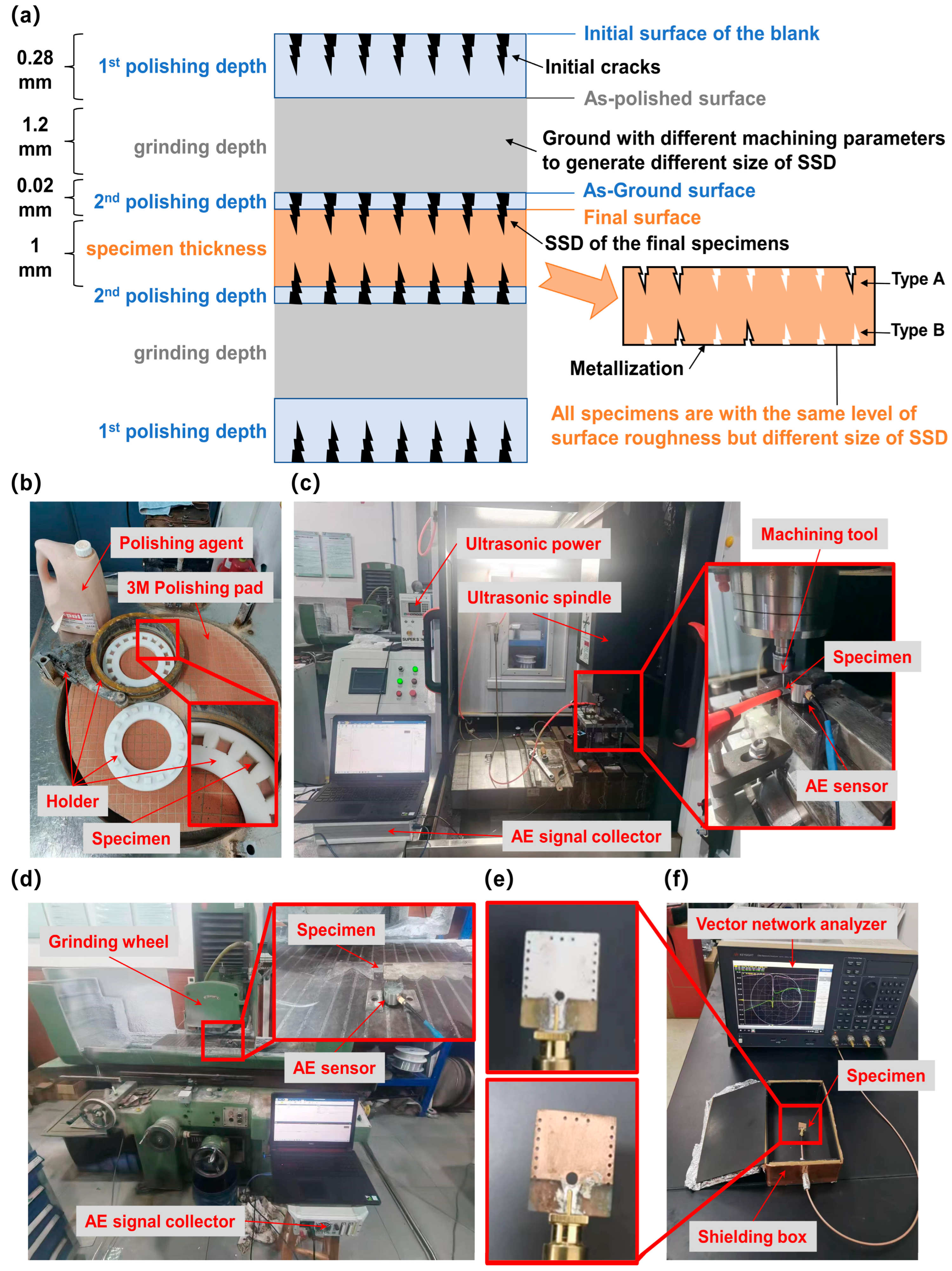
To assess the impact of the SSD resulting from machining on the frequency offset, an experimental processing plan was devised, as depicted in Figure 2. The plan aimed to generate varying SSD sizes through the manipulation of different processing parameters. The sintered raw material was cut using emery wire cutting machine and subsequently ground into blanks with dimensions of 14 mm × 16.5 mm × 3 mm. The mechanical properties of the quartz ceramic are listed in Table 1 [23].
The critical depth dc of the ductile–brittle transition in grinding processes can be determined using (1); the critical depth serves as a criterion to ascertain whether the material removal mode in a grinding process is ductile or brittle. A brittle grinding process tends to induce more severe SSD on the ground surfaces compared to ductile processes [47].
d c = 8.7 H E · K C H = 28.55 nm
Figure 2a illustrates the various surface processing steps. The initial surfaces of the blanks underwent a 0.28 mm single-side depth polishing process (using the machine shown in Figure 2b). This process aimed to eliminate the initial cracks generated during the preceding cutting and grinding processes. Subsequently, the through holes were drilled using two methods to induce SSD with varying sizes on the hole walls: (A) utilizing an ultrasonic assisted machining system with polycrystalline diamond (PCD) cutting tools (shown in Figure 2c); and (B) employing a conventional drilling machine with electroplated diamond bits. It has been demonstrated that ultrasonically assisted machining can effectively reduce SSD among hard and brittle materials [41,48,49].
Two sets of distinct machining parameters, which are listed in Table 2, were adopted in the following process to remove a total single-side depth of 1.2 mm. This aimed to create SSD of different sizes on the upper and lower surfaces (using the machine shown in Figure 2d).
The maximum undeformed chip thickness Hm of each grinding parameter can be calculated through (2) [50]:
H m = 4 v w v s · C · r d g d w 0.5 ,
where vs is linear speed of the grinding wheel, C = 475 mm−2 is the number of active grits per unit area on the 600# wheel surface, and r = 15 is the chip width/thickness ratio.
For the set of grinding parameters No. 1, Hm = 24.1 nm, which is below the dc. This indicates a ductile grinding process likely resulting in reduced SSD. Conversely, for the set of parameters No. 2, Hm = 34.1 nm, indicating a brittle material removal process with more pronounced SSD.
Subsequently, the specimens underwent another round of polishing, this time with a 0.02 mm single-side depth, to achieve a consistent surface roughness (Ra = 0.1 µm). Finally, the specimens with a thickness of 1 ± 0.005 mm were metallized through two methods: (1) the silver method, i.e., silver paste printing; (2) the copper method, i.e., metal spraying and electro-coppering (shown in Figure 2e).
In the silver method, silver paste was applied to the quartz through a silk screen and dried at 150 °C for 10 min. Subsequently, the specimens underwent a sintering process by heating to 800 °C in a muffle furnace for 20 min. It is noteworthy that the phase transition point of quartz exceeds 1100 degrees, ensuring that the drying and sintering processes do not induce changes in the quartz matrix or the cracks in their subsurface.
In the copper method, gold ions were excited and then sputtered onto the surfaces of the quartz specimens using high voltage with gold-spraying equipment commonly employed in sample production for scanning electron microscopy. The maximum process temperature did not exceed 80 °C. Following this, the quartz underwent a copper electroplating process at room temperature. In summary, the two metallization methods employed in this process were designed to avoid introducing additional cracks or defects on the ceramic surfaces.
An acoustic emission (AE) sensor (Fuji 1045S, Fujicera, Shizuoka, Japan) was used to monitor the sound signals emitted during both the drilling and grinding processes. Analyzing the characteristics of the AE signals in the frequency domain proves valuable in understanding the severity of SSD [51].
A laser process was employed to eliminate the unwanted metallization, forming the patten shown in Figure 1a. The precision of the patten was measured using the VHX-7000 digital microscope, yielding a precision result of less than 0.01 mm. SMA-type connectors were soldered onto the specimens and connected to a vector network analyzer (VNA; Keysight E5071C-4K5; from 300 kHz to 20 GHz with bias tees; calibrated using a Keysight 85052D 3.5 mm economy calibration kit). This setup facilitated the measurement of the resonant frequency of the specimens (shown in Figure 2f).

3. Experimental Result

3.1. Observation and Measurement of the SSD

Figure 3a–c illustrates the AE signals of the grinding and drilling processes in the frequency domain. Notably, when employing the set of parameters No. 2 for grinding (Figure 3c), a distinct peak emerges around 18 kHz, signifying a brittle material removal process associated with more severe SSD. Figure 3d,e shows the cross section of the final surfaces after machining. Set of parameters No. 2 leads to more pronounced SSD with a depth of approximately 89 um, while set of parameters No. 1 yields a depth of about 13 um. Six SIW resonators were fabricated for each set of the machining parameters listed in Table 2. Three of them were metallized using the silver method, while the remaining three were metallized using the copper method. Comparing Figure 3f–i, it can be inferred that copper metallization more readily invades the cracks than the silver method. Moreover, Figure 3f,h indicate that neither the silver nor the copper metallization processes introduce additional cracks or defects on the surfaces. Figure 3g,i depicted that the morphology and size of cracks remained unaffected by the metallization process.

3.2. Measured Frequency Offsets Induced by SSD

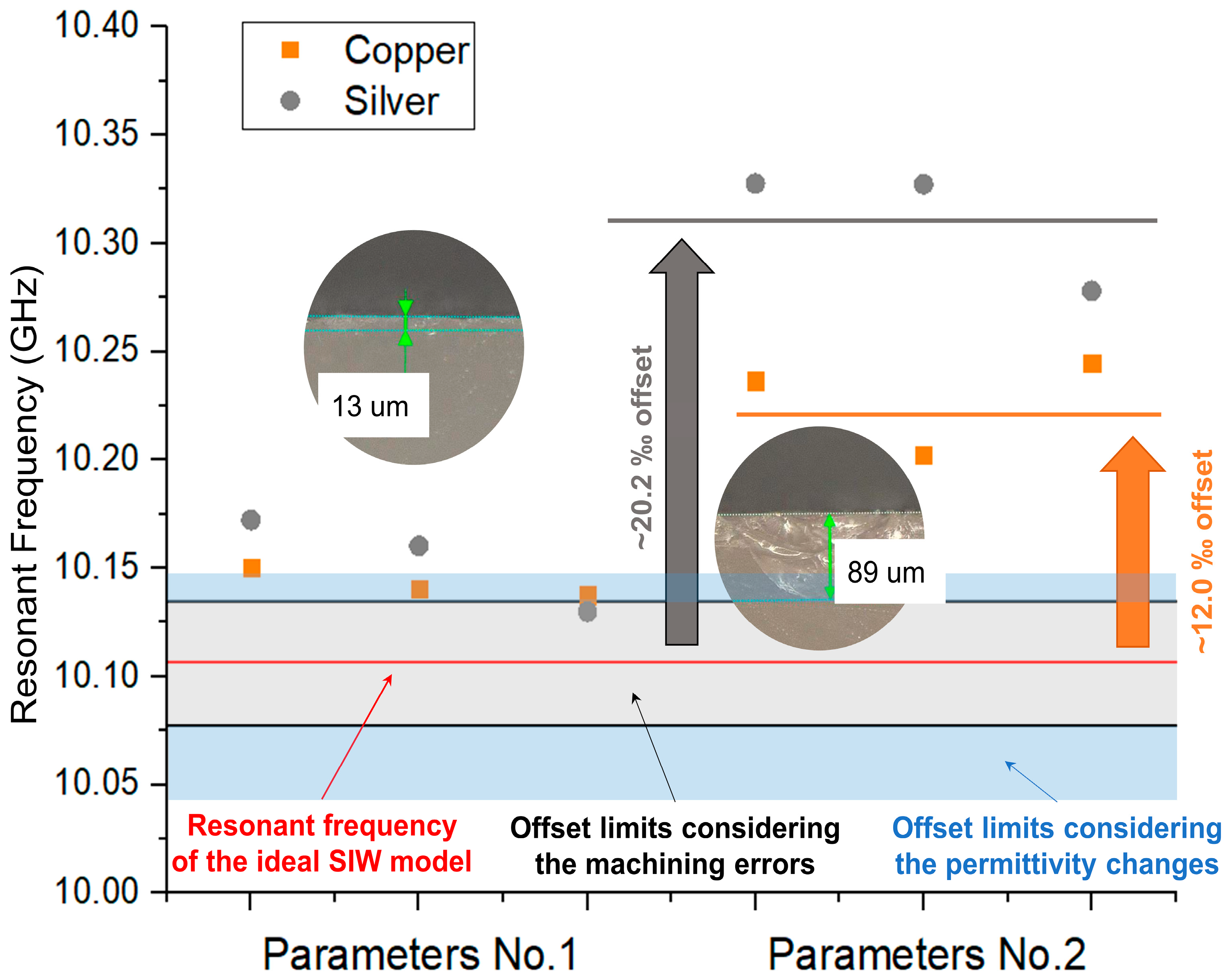
The measured frequency results are illustrated in Figure 4 (see Appendix A for detailed information), with the grey and blue region indicating the limit frequency shift caused by machining errors and permittivity changes (see Section 2.1). The illustration clearly demonstrates that more severe machining conditions lead to a larger size of SSD, resulting in a correspondingly larger frequency offset. Among the six resonators machined using set of parameters No. 1, their resonant frequencies all exhibited a positive divergence in one direction from the expected mean value. This phenomenon indicated that, even with a moderate manufacturing process, the induced SSD could cause more significant frequency offsets than the size errors and the permittivity changes. Resonators manufactured using set of parameters No. 2 exhibited more obvious frequency offsets: for the specimens metallized using the copper method, SSD induced an average offset of 12.0%, while this number increased to 20.2% for those metallized with silver. It can be inferred that different metallization methods also exert different influences on the frequency offset.

3.3. Impacts of SSD on System Performance

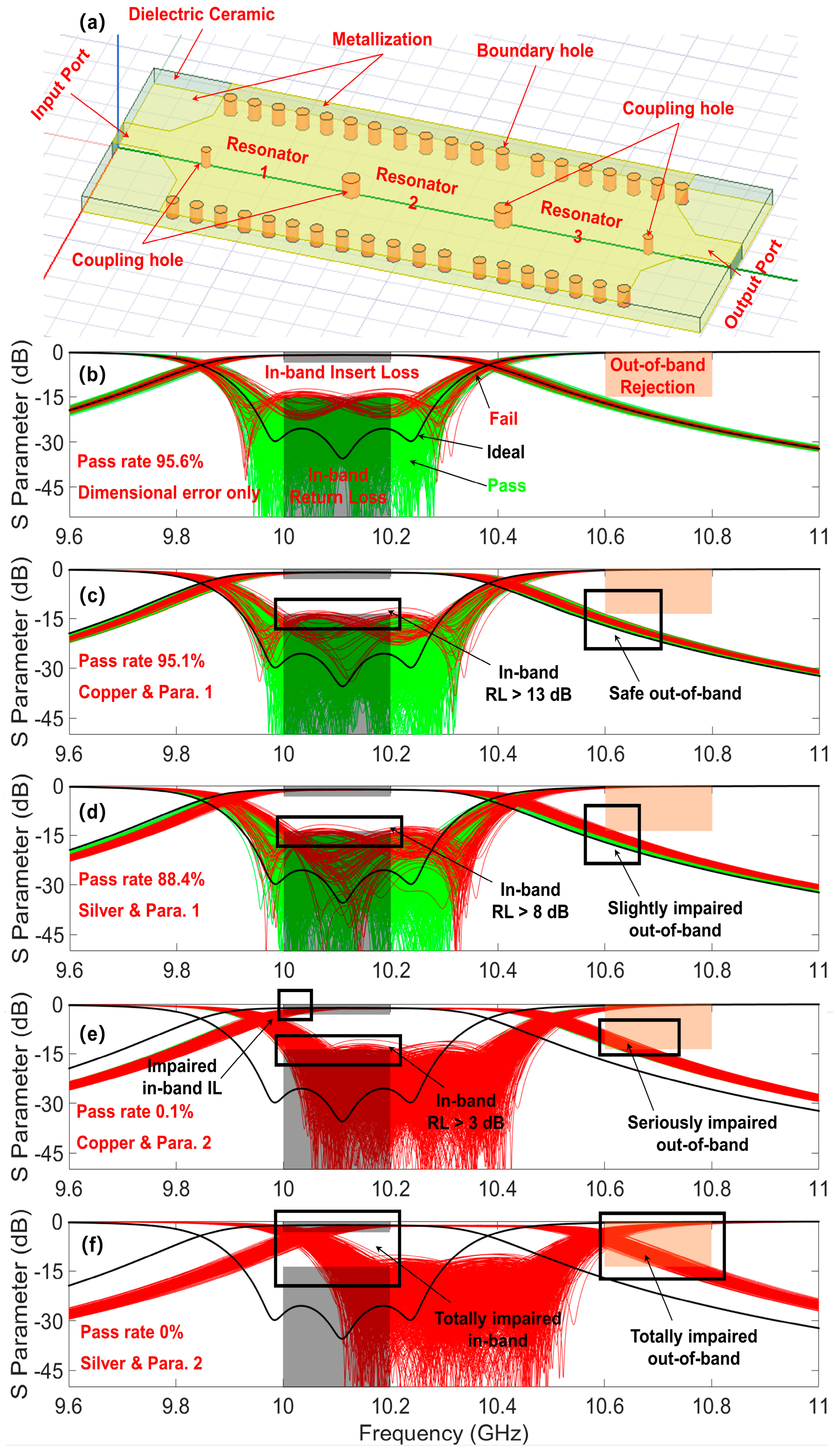
The frequency offset caused by SSD can have subsequent implications on the system performance when a resonator is integrated into a microwave system, as exemplified by the filter illustrated in Figure 5.
Figure 5a showcases a three-cavity bandpass filter composed of the SIW resonators fabricated in this study. The filter is designed with a passband spanning from 10 to 10.2 GHz (with a bandwidth of 200 MHz), a stopband ranging from 10.6 to 10.8 GHz, an in-band return loss (RL) > 15 dB, an in-band insert loss (IL) < 2 dB, and an out-of-band rejection > 15 dB. Figure 5b–f illustrate the S parameters of the model, considering errors in the dimensions and the resonators affected by SSD.
Table 3 lists the average (Aver.) and standard deviation (STD.) of the cavity-resonant frequency in each case (see Appendix A for detailed information).
The calculation steps for deriving the S parameters in Figure 5 based on the provided statistical data are outlined as follows.
  • In each case, generate 3000 cavities, with frequencies following a normal distribution by an expectation value of Aver. Freq. and a standard deviation of STD Freq., as listed in Table 3.
  • Randomly select three cavities from the pool of 3000 to form a three-cavity filter. Repeat this selection and forming process 1000 times, resulting in a total of 1000 generated filters.
  • Calculate the S parameters of each filter.
  • Plot the S parameters in a figure, where the green line indicates that the corresponding filter meets the specified requirements, while the red line signifies that the filter does not qualify.
Figure 5b illustrates the simulated S parameters of the ideal filters, influenced by errors in dimensions but not subjected to SSD. Out of the 1000 randomly generated filters, the pass rate reaches 95.6%. Any unsuitable filters are attributed to the in-band RL slightly exceeding the required value.
In Figure 5c, the S parameters of the copper-metalized filters subjected to grinding with the set of parameters No. 1 are depicted. The 95.1% pass rate indicates that adequate metallization and appropriate machining processes can effectively mitigate the adverse effects of SSD.
Figure 5d illustrates that the silver metallization is less stable than the copper method, resulting in a reduced pass rate of 88.4%.
Figure 5e,f show the results for set of grinding parameters No. 2. The frequency offsets induced by more serious SSD lead to the failure of all the filters. The SSD impaired 37.57% of the passband and 48.68% of the stopband for a copper-metalized filter when fabricated using set of machining parameters No. 2. For a silver-metalized one, both the passband and stopband are impacted by 100%.

4. Theoretic Analysis on Mechanism

4.1. Discussion on General Cases

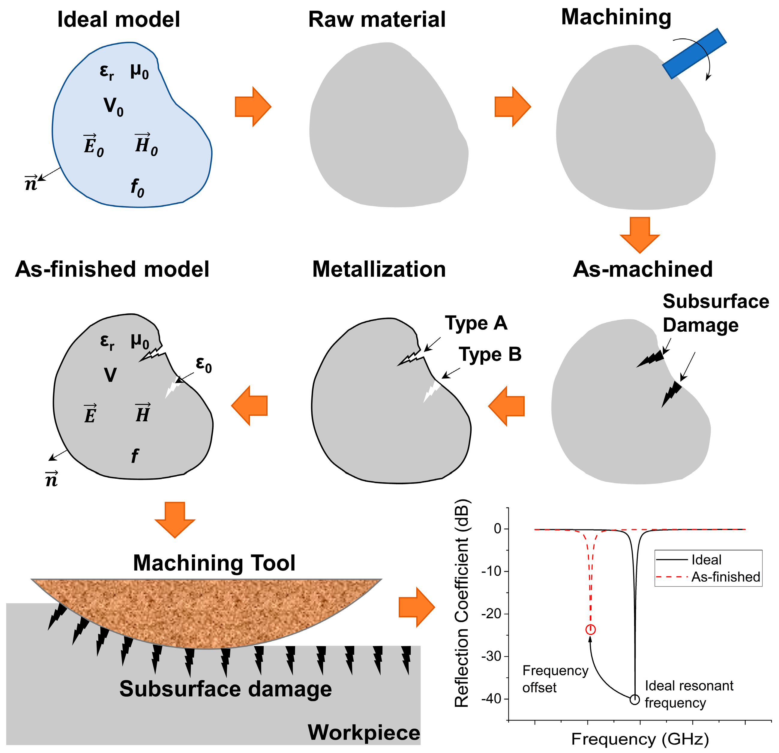
Figure 6 shows the logic principle behind the frequency offset induced by SSD. The depicted cavity has an irregular shape to emphasize that the theory is not limited only to specific component shapes. The outline of the ideal model is V0, which is made of an MWDC with a relative permittivity εr. As the component guides electromagnetic waves, the electric and magnetic fields inside are denoted as E 0 and H 0 , respectively, and the resonant frequency is f0. The component is fabricated from raw materials and undergoes machining processes to achieve precise dimensions, during which SSD may be induced. Upon metallization, the damage can be categorized into two types: Type A, in which the surface of the crack is filled with metal, and Type B, where the crack is covered by metal, leaving its surface nonmetallized. The perturbation theory can be employed to analyze the frequency offset caused by these cracks.
For Type A damage, the component loses the volume of the crack, which leads to a perturbation of the shape of the resonant cavity. This shape perturbation results in a deviation of the working frequency of the cavity from f0 to f = f0 +f. The frequency offset ratio ∆f/f0 can be calculated using (3) [52].
f f 0 = V   ε 0 ε r E 0 · E 0   *   μ 0 H 0 * · H 0 d V V 0   ε 0 ε r E · E 0 * +   μ 0 H 0 * · H d V ,
where ∆V is the volume of the crack, and ε0 is the permittivity of the vacuum.
For Type B damage, the volume of the component remains unchanged. However, the material within the range of the crack changes from ceramic to air, which has a relative permittivity εair. This results in a material perturbation that causes a frequency offset; the corresponding frequency offset ratio is calculated using (4) [52].
f f 0 = V   ε 0 ε a i r   ε 0 ε r E 0 · E 0 d V V 0   ε 0 ε r E · E 0 + μ 0 H 0 · H d V ,
It is crucial to note that the influence of Type A damage is directly linked to its location: if the damage appears in an area where the energy of the electric field surpasses that of the magnetic field, it causes a negative frequency shift, resulting in a lower resonant frequency, and vice versa. Meanwhile, given that the permittivity of ceramics is consistently greater than that of air, Type B damage typically leads to positive frequency offsets.
During machining processes, a multitude of SSD is generated. Some of the cracks evolve into Type A damage, while the others become Type B. The total frequency offset ratio can be calculated through summing up the effects of all the cracks, as in (5).
f t o t a l f 0 = t y p e   A f i f 0 + t y p e   B f j f 0 ,
It can be empirically inferred that metallizing processes utilizing small metal particles, such as magnetron sputtering and chemical plating, tend to induce Type A SSD (e.g., the copper method in our experiments). On the other hand, processes like copper-foil covering and silk-screen printing make it more challenging for the metal to fill the cracks, leading to the appearance of Type B SSD (as observed in the silver method). It can be derived below that the effect of a Type A crack is smaller than Type B for a rectangular resonator. This observation provides an explanation for why different metallizing processes lead to different frequency offset in the experiments.

4.2. Discussion on the SIW in the Experiments

For the SIW resonators used in the experiments, it can be equivalent to a rectangular resonator working in TE101 mode, whose length, width, and height are X, Y, and Z [(Z < min(X, Y)], respectively. The following conclusions can be made (with the detailed derivation found in Appendix B):
  • If all cracks are of Type A, then the induced frequency offset is calculated through (A9).
  • If all cracks are of Type B, then (A10) can be employed.
where α = Y / X is the length ratio of the two sides, and D e s is the average distance between every two cracks. In practice, measuring V and D e s is challenging based on existing technologies, despite numerous studies [37,42,53] that have focused on measuring and predicting the depth of SSD, rather than its volume and distance. Considering the substantial impact of SSD on the performance of microwave devices discussed in this paper, future research should explore technical methods to measure the volume and distance of each crack, providing statistical information for a more comprehensive understanding of the phenomenon.
At the present stage, V and D e s remain conceptual parameters in the theoretical derivation, highlighting the notion that larger and more intensive the cracks have a more pronounced impact on the frequency performance of the components. Therefore, the frequency offset ratio of an actual component with SSD should fall within the ranges specified by (A9) and (A10):
f t o t a l   A f 0 < f C o p p e r f 0 < f S i l v e r f 0 < f t o t a l   B f 0 ,
where the relationship f t o t a l   A / f 0 < f t o t a l   B / f 0 can be seen in the discussion in Section 4.3.

4.3. Discussion on SA and SB

Both (A9) and (A10) contain two terms: the former ( S A = 4 1 + α 3 · μ 0 ε 0 ε r · f 0 1 + α 2 3 / 2 Z and S B = ε r ε a i r ε r Z ) depends solely on the physical structure of the component; the latter ( V / D e s and V / D e s 2 ) represents the severity of the SSD, which is further influenced by the toughness of the ceramics and the machining parameters. Resonator structures with larger SA will experience a more significant frequency offset for given Type A damage, and vice versa. Conversely, utilizing fine and moderate machining processes on tougher materials can help decrease ∆V and increase Des, thereby minimizing the frequency deviation of a resonator with a specific structure.
According to (12) and (13), both SA and SB are inversely proportional to Z. Moreover, the two length ratios α , which are reciprocal of each other, contribute the same amount to SA [ 1 + α 3 / 1 + α 2 3 / 2 = 1 + 1 / α 3 / 1 + 1 / α 2 3 / 2 ]. Figure 7 illustrates the calculation results of SA and SB with different parameters.
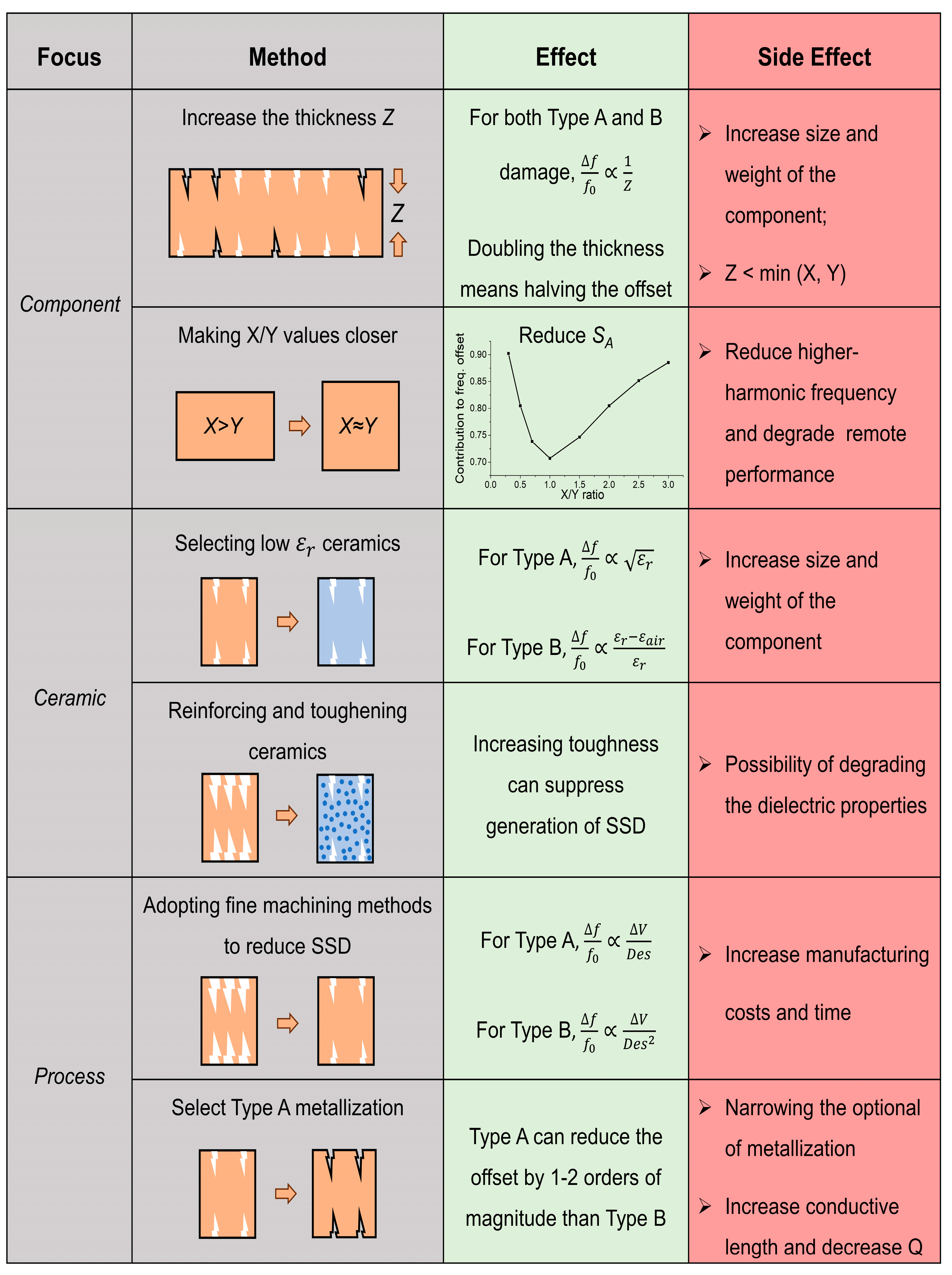
As depicted in Figure 7, for a given value of Z, a rise in both f0 and εr results in an increment in SA, while SB is solely determined by εr. As εr increases, SB gradually approaches its limit value, 1/Z. This implies that the pursuit of high-frequency and miniaturized waveguide components will make them more sensitive to SSD. On the other hand, for a given resonant frequency f0, a resonator with a smaller εr, a larger Z, and an α close to 1 will be less sensitive to the SSD effect. However, these approaches also have side effects: a smaller εr and a larger Z will inevitably increase the size of the component, while an α close to 1 can reduce the high-mode harmonic frequency, potentially degrading the high-frequency performance of the system.
Table 4 presents the frequency offset on different resonators with SSD. If all cracks are of Type B, then calculated frequency offset is 31.7% for the SIW resonator used in the experiments (see the third row of Table 4 and Appendix A for detailed information). Comparing this with the experimental offset results, i.e., 12.0% for the copper method and 20.2% for the silver method, our explicit physical analysis Equation (6) is consistent with the reality (see Appendix A for detail). Moreover, the effect on the frequency offset is larger by 1–2 orders of magnitude in the case when all cracks are of Type B compared to the case when all cracks are of Type A. Additionally, even if all cracks are of Type A, the frequency offset ratio is 1.7–39.4% at a working frequency of 70 GHz. This effect is still significant compared to the system bandwidth, which is generally in the range of 0.5–10% of the center frequency. In summary, SSD can cause a substantial performance decrease, especially in the cases of high-frequency and miniaturized devices. Therefore, SSD should be carefully considered in the design and manufacturing of waveguide components.

4.4. Methods to Reduce the Offset Induced by SSD

The discussion above clearly demonstrates that the impact of the SSD on the resonant frequency can be mitigated or suppressed through targeted design and suitable fabrication methods. For the rectangular resonator, the methods are summarized in Figure 8. However, it is important to note that each method comes with side effects that may potentially reduce the performance of the device in other aspects. The specific method to be implemented in practical engineering needs to be determined by balancing various actual requirements.

5. Conclusions

  • This study presents, for the first time, the impact of SSD on the frequency performance of ceramic waveguide components, experimentally confirming a maximum frequency offset of 20.2% at 10.1 GHz and theoretically calculating a maximum frequency offset of 176% at 70 GHz.
  • The perturbation method is introduced to conceptually explain why SSD can cause a frequency offset in a ceramic waveguide component. The derivation provides a quantitative estimation of the limiting range of the offset caused by given SSD, demonstrating that miniaturized resonators working at high frequencies are more affected.
  • The rationalized design of waveguided components can decrease sensitivity to SSD, while optimized processing can reduce the size of SSD. Metallization processes using smaller particles are also beneficial. These considerations are crucial for advanced applications of ceramic devices in high-performance communication and frequency control systems.
  • This work exemplifies the interdisciplinary intersection of microwave engineering, materials science, and manufacturing technology. It highlights that only by combining electromagnetic design methods, high-performance materials, and optimized machining processes, can high-quality and highly reliable microwave components be produced. This research paves the way for further interdisciplinary studies on microwave semiconductor components and systems. Methods for measuring the volume and density of SSD are also anticipated.

Author Contributions

Conceptualization, H.W., J.W. and T.S.; methodology, H.W.; software, X.C. and J.D.; validation, H.W., X.C. and H.H.; formal analysis, J.W. and Z.F.; writing, H.W.; visualization, J.W.; supervision, B.L. All authors have read and agreed to the published version of the manuscript.

Funding

This work was supported by the National Natural Science Foundation of China under Grant Nos. 52275458 and 52275207, and the Natural Science Foundation of Tianjin under Grant No. 22JCZDJC00050.

Data Availability Statement

The data that support the findings of this study are available from the corresponding authors upon reasonable request.

Acknowledgments

The authors wish to thank Jinyuan Wang and Shigang Dai for helping prepare the specimens for the experiments. This paper has been carefully edited by MogoEdit (https://mogoedit.com/, accessed on 11 November 2023), and the grammar, spelling, and punctuation have been verified and corrected where needed.

Conflicts of Interest

The authors declare no conflict of interest.

Appendix A. Detailed Statistical Information

The frequency data of the simulation in both experimental and calculated instances are shown in Table A1.
Table A1. Frequency data of all the instances in the paper.
Type of
Instance
ConditionsResonant
Frequency
(GHz)
Frequency
Offset
(%)
Average
Offset
(%)
STD.
Offset
(%)
Data
Application
Size
Error
SSDMetallization
SimulationNoNoIdeal10.106500-Figure 1c
YesNoIdeal10.0773−2.88920.30251.5418Figure 1e
Table 3
10.092−1.4347
10.0997−0.6728
10.1032−0.3265
10.1053−0.1187
10.10740.089
10.11020.3661
10.1130.6431
10.11440.7816
10.12842.1669
10.12912.2361
10.13472.7902
ExperimentYesPara.
No. 1
Silver10.172306.51064.72291.755Figure 4
Table 3
10.160275.3203
10.130132.338
YesPara.
No. 1
Copper10.150094.3133.59530.5227
10.140763.3898
10.137663.0831
YesPara.
No. 2
Silver10.3275821.87520.22652.3047
10.3272021.8374
10.2779816.9672
YesPara.
No. 2
Copper10.2366012.872912.01271.8152
10.202399.4879
10.2447313.6773
CalculationNoV = 4 × 10⁻⁵ mm3 and Des = 0.03 mmIf all cracks are Type A--0.25-Table 4
If all cracks are Type B--31.7-

Appendix B. Detailed Perturbation Derivation for the SIW Resonator with SSD

Firstly, some Lemmas are discussed, as follows:
Set n = X/Des is the number of the summation terms. Considering Lemma 1,
Lemma 1.
k = 0 n e i k x = k = 0 n cos k x + i sin k x , k = 0 n cos k x = R e k = 0 n e i k x
k = 0 n e i k x = 1 e i n + 1 x 1 e i x = sin n + 1 x 2 sin x 2 e i n x 2 = sin n + 1 x 2 sin x 2 cos n x 2 + i sin n x 2
k = 0 n cos k x = R e k = 0 n e i k x = sin n + 1 x 2 sin x 2 cos n x 2 = sin n + 1 2 x + sin x 2 2 sin x 2
one can come to Lemma 2,
Lemma 2.
s i n 2 π X x i = k = 1 n s i n 2 2 π k n = k = 1 n 1 2 1 cos 2 π k n = n 2 1 2 k = 1 n cos 2 π k n = n 2 1 2 k = 0 n cos 2 π k n cos 0 = n 2 1 2 sin n + 1 2 2 π n + sin π n 2 sin π n cos 0 = n 2 1 2 sin π n + 2 π + sin π n 2 sin π n cos 0 = n 2 = X 2 D e s
Lemma 3,
Lemma 3.
c o s 2 π X x i = k = 1 n c o s 2 2 π k n = k = 1 n 1 s i n 2 2 π k n = n n 2 = n 2 = X 2 D e s
and Lemma 4,
Lemma 4.
s i n 2 π X x i s i n 2 π Y y j = l = 1 n 1 k = 1 n 2 s i n 2 2 π k n 2 s i n 2 2 π l n 1 = l = 1 n 1 s i n 2 2 π l n 1 k = 1 n 2 s i n 2 2 π k n 2 = l = 1 n s i n 2 2 π l n 2 n 1 2 = n 2 n 1 4 = X Y 4 D e s 2 .
Then, one can come to the physical analysis of the SIW cavity, whose length, width, and height of the equivalent rectangular resonator working in TE101 mode are X, Y, and Z [(Z < min (X, Y)], respectively. The explicit expressions of its E 0 and H 0 (the directional scalars that are not listed are equal to zero) can be derived as [53]:
E 0 z = E 0 sin π X x s i n ( π Y y ) H 0 x = j E 0 η λ 0 2 Y sin π X x c o s ( π Y y ) H 0 y = j E 0 η λ 0 2 X cos π X x s i n ( π Y y ) ,
where η = μ 0 / ( ε 0 ε r ) is the wave impedance, λ 0 = c / f 0 = 2 X Y / X 2 + Y 2 is the wave length of the resonant frequency, and c = 1 / μ 0 ε 0 ε r is the speed of light.
Different machining parameters lead to different SSD sizes. In a hypothetical case that all cracks are equally sized and evenly distributed on all the six surfaces, the corresponding frequency offset ratios can be calculated based on the assumption that all cracks are Type A or Type B during metallization.
  • For the condition that all cracks are Type A:
f t o t a l f 0 = 2 s i n 2 ( π X x i ) s i n 2 ( π Y y j ) X 2 X 2 + Y 2 s i n 2 ( π X x i ) c o s 2 ( π Y y j ) Y 2 X 2 + Y 2 c o s 2 ( π X x i ) s i n 2 ( π Y y j ) · V X Y Z
  • For the condition that all cracks are Type B:
f t o t a l f 0 = 2 ε r ε a i r s i n 2 ( π X x i ) s i n 2 ( π Y y j ) · V ε r X Y Z
In the above cases, because the cracks are relatively small, the amplitude of the fields are treated to be uniform so that the integrals are converted into multiplications. Thus, xi and yi are the coordinate values of each crack.
Using the following (A4)–(A6), which can be easily derived from Lemma 2–4, (A2) and (A3) can be further simplified.
  • On the top and bottom surfaces (xy plane, z = 0 and z = Z):
s i n 2 π X x i s i n 2 π Y y j = c o s 2 π X x i s i n 2 π Y y j = s i n 2 ( π X x i ) c o s 2 ( π Y y j ) = X Y 4 D e s 2 ,
  • On the left and right surfaces (xz plane, y = 0 and y = Y):
s i n 2 π X x i s i n 2 π Y y j = c o s 2 π X x i s i n 2 π Y y j = 0 s i n 2 ( π X x i ) c o s 2 ( π Y y j ) = X 2 D e s ,
  • On the front and back surfaces (yz plane, x = 0 and x = X):
s i n 2 ( π X x i ) s i n 2 ( π Y y j ) = s i n 2 π X x i c o s 2 π Y y j = 0 c o s 2 ( π X x i ) s i n 2 ( π Y y j ) = Y 2 D e s ,
Using (A4)–(A6), (A2) and (A3), we have:
  • If all cracks are Type A, then
f t o t a l   A f 0 = 2 X 3 + Y 3 X 2 + Y 2 X Y Z · V D e s = 2 1 + α 3 1 + α 2 Y Z · V D e s ,
where α = Y / X is the length ratio of the two sides, which is usually set as 1/3 ≤ α ≤ 3 for general rectangular resonator design.
While designing a resonator, the expected resonant frequency f0 is a known condition. According to Equation (A1), we have:
Y = 1 + α 2 2 μ 0 ε 0 ε r · f 0 ,
Taking (A8) into (A7), we have:
f t o t a l   A f 0 = 4 1 + α 3 · μ 0 ε 0 ε r · f 0 1 + α 2 3 / 2 Z · V D e s = S A · V D e s ,
  • If all cracks are Type B, then
f t o t a l   B f 0 = ε r ε a i r ε r Z · V D e s 2 = S B · V D e s 2

References

  1. Ohsato, H.; Tsunooka, T.; Sugiyama, T.; Kakimoto, K.-I.; Ogawa, H. Forsterite ceramics for millimeterwave dielectrics. J. Electroceram. 2006, 17, 445–450. [Google Scholar] [CrossRef]
  2. Yang, H.; Zhang, S.; Yang, H.; Wen, Q.; Yang, Q.; Gui, L.; Zhao, Q.; Li, E. The latest process and challenges of microwave dielectric ceramics based on pseudo phase diagrams. J. Adv. Ceram. 2021, 10, 885–932. [Google Scholar] [CrossRef]
  3. Ermawati, F.U. The Response of (Mg0.6Zn0.4)TiO3 Ceramic System as A Dielectric Resonator Oscillator at C-Band. J. Phys. Conf. Ser. 2021, 1805, 012039. [Google Scholar] [CrossRef]
  4. Ni, L.; Li, L.; Du, M.; Zhan, Y. Wide temperature stable Ba(MgxTa2/3)O3 microwave dielectric ceramics with ultra-high-Q applied for 5G dielectric filter. Ceram. Int. 2021, 47, 1034–1039. [Google Scholar] [CrossRef]
  5. Zhou, M.F.; Hu, C.C.; Yin, J.B.; Jiang, Y.; Liu, B.; Song, K.X. Cold sintering optimized SrF2 microwave dielectric ceramics for the development of dielectric resonator antenna at 5G millimeter-wave band. Ceram. Int. 2022, 48, 29847–29853. [Google Scholar] [CrossRef]
  6. Chen, Y.-C.; Weng, M.-Z.; Du, Y.-X.; Hsiao, C.-L. Microwave dielectric properties of Nd(Ti0.5−xZrx)W0.5O4 ceramics for application in antenna temperature sensor. J. Mater. Sci. Mater. Electron. 2018, 29, 4717–4723. [Google Scholar] [CrossRef]
  7. Kazemi, N.; Abdolrazzaghi, M.; Light, P.E.; Musilek, P. In–human testing of a non-invasive continuous low–energy microwave glucose sensor with advanced machine learning capabilities. Biosens. Bioelectron. 2023, 241, 115668. [Google Scholar] [CrossRef]
  8. Abdolrazzaghi, M.; Kazemi, N.; Nayyeri, V.; Martin, F. AI-Assisted Ultra-High-Sensitivity/Resolution Active-Coupled CSRR-Based Sensor with Embedded Selectivity. Sensors 2023, 23, 6236. [Google Scholar] [CrossRef]
  9. Kamutzki, F.; Schneider, S.; Barowski, J.; Gurlo, A.; Hanaor, D.A.H. Silicate dielectric ceramics for millimetre wave applications. J. Eur. Ceram. Soc. 2021, 41, 3879–3894. [Google Scholar] [CrossRef]
  10. Narang, S.B.; Bahel, S. Low loss dielectric ceramics for microwave applications: A review. J. Ceram. Process. Res. 2010, 11, 316–321. [Google Scholar]
  11. Abdolrazzaghi, M.; Nayyeri, V.; Martin, F. Techniques to Improve the Performance of Planar Microwave Sensors: A Review and Recent Developments. Sensors 2022, 22, 6946. [Google Scholar] [CrossRef] [PubMed]
  12. Basu, J.; Bhattacharyya, T.K. Microelectromechanical resonators for radio frequency communication applications. Microsyst. Technol. 2011, 17, 1557. [Google Scholar] [CrossRef]
  13. Zhai, W.; Xin, Y.; Xie, M.; Zhao, M.; Huang, S. Phase noise suppression for RF signal remote fiber transmission using phase balance compensation feedback network in phase shifter. Optik 2019, 177, 131–135. [Google Scholar] [CrossRef]
  14. Wang, J.; Chen, X.M.; Yang, J.S. Temperature-stable dielectric ceramics in Ba4Nd2Ti4Ta6O30/(La0.1Bi0.9)2Ti2O7 biphase system. J. Mater. Res. 1999, 14, 3375–3378. [Google Scholar] [CrossRef]
  15. Wang, K.; Zhou, H.; Luan, X.; Hu, S.; Zhou, X.; He, S.; Wang, X.; Zhou, S.; Chen, X. NaTaO3 microwave dielectric ceramic a with high relative permittivity and as an excellent compensator for the temperature coefficient of resonant frequency. Ceram. Int. 2021, 47, 121–129. [Google Scholar] [CrossRef]
  16. Dou, Z.; Wang, G.; Jiang, J.; Zhang, F.; Zhang, T. Understanding microwave dielectric properties of (1−x)CaTiO3–xLaAlO3 ceramics in terms of A/B-site ionic-parameters. J. Adv. Ceram. 2017, 6, 20–26. [Google Scholar] [CrossRef]
  17. Wang, H.; Zhou, F.; Guo, J.; Zhang, Y.; Yang, H.; Zhang, Q. Surface-modified Zn0.5Ti0.5NbO4 particles filled polytetrafluoroethylene composite with extremely low dielectric loss and stable temperature dependence. J. Adv. Ceram. 2020, 9, 726–738. [Google Scholar] [CrossRef]
  18. Teberio, F.; Gomez-Torrent, A.; Arregui, I.; Percaz, J.M.; Arnedo, I.; Chudzik, M.; Lopetegi, T.; Laso, M.A.G. Sensitivity analysis of a 3-D printed low-cost compact waveguide low-pass filter. In Proceedings of the EuMW 2016—Conference Proceedings; 46th European Microwave Conference, EuMC, London, UK, 4–6 October 2016; European Microwave Week 2016: “Microwaves Everywhere”. pp. 249–252. [Google Scholar]
  19. Teberio, F.; Soto, P.; Arregui, I.; Lopetegi, T.; Cogollos, S.; Arnedo, I.; Martin-Iglesias, P.; Boria, V.E.; Laso, M.A.G. Waveguide band-pass filter with reduced sensitivity to fabrication tolerances for Q-band payloads. In Proceedings of the IEEE MTT-S International Microwave Symposium Digest, Honolulu, HI, USA, 4–9 June 2017; pp. 1464–1467. [Google Scholar]
  20. Yang, H.; Dhayalan, Y.; Shang, X.; Lancaster, M.J.; Liu, B.; Wang, H.; Henry, M.; Huggard, P.G. WR-3 Waveguide Bandpass Filters Fabricated Using High Precision CNC Machining and SU-8 Photoresist Technology. IEEE Trans. Terahertz Sci. Technol. 2018, 8, 100–107. [Google Scholar] [CrossRef]
  21. Wang, H.; Wei, J.; Lin, B.; Zhang, Y.; Hou, H.; Sui, T. Ultraprecise Resonant Frequency Prediction of Microwave Cavities with Deformations. IEEE Trans. Microw. Theory Tech. 2023, 1–10. [Google Scholar] [CrossRef]
  22. Zhang, B.; Yin, J. The ‘skin effect’ of subsurface damage distribution in materials subjected to high-speed machining. Int. J. Extrem. Manuf. 2019, 1, 012007. [Google Scholar] [CrossRef]
  23. Bin, L.; Junpeng, Z.; Zhong-Chen, C.; Jiannan, Z.; Tian, H. Theoretical and experimental investigation on surface generation and subsurface damage in fixed abrasive lapping of optical glass. Int. J. Mech. Sci. 2022, 215, 106941. [Google Scholar] [CrossRef]
  24. Jiwang, Y.; Xiaohui, G.; Hirofumi, H. Subsurface damage of single crystalline silicon carbide in nanoindentation tests. J. Nanosci. Nanotechnol. 2010, 10, 7808–7811. [Google Scholar]
  25. Li, H.N.; Yu, T.B.; Zhu, L.D.; Wang, W.S. Analytical modeling of grinding-induced subsurface damage in monocrystalline silicon. Mater. Des. 2017, 130, 250–262. [Google Scholar] [CrossRef]
  26. Huang, J.; Zhou, X.; Liu, H.; Wang, F.; Jiang, X.; Wu, W.; Tang, Y.; Zheng, W. Influence of subsurface defects on damage performance of fused silica in ultraviolet laser. Opt. Eng. 2013, 52, 024203. [Google Scholar] [CrossRef]
  27. Chunyang, W.; Rongting, G.; Xuelian, L.; Yana, C.; Tiantian, L. Study on the relationship between the fluorescence characteristics of quantum dots and the subsurface damage of fused silica. In Proceedings of the 2021 IEEE International Conference on Manipulation, Manufacturing and Measurement on the Nanoscale (3M-NANO), Xi’an, China, 2–6 August 2021; pp. 258–263. [Google Scholar]
  28. Kakinuma, Y.; Azami, S.; Tanabe, T. Evaluation of subsurface damage caused by ultra-precision turning in fabrication of CaF2 optical micro resonator. CIRP Ann. 2015, 64, 117–120. [Google Scholar] [CrossRef]
  29. Mazzù, A.; Solazzi, L.; Lancini, M.; Petrogalli, C.; Ghidini, A.; Faccoli, M. An experimental procedure for surface damage assessment in railway wheel and rail steels. Wear 2015, 342–343, 22–32. [Google Scholar] [CrossRef]
  30. Levikari, S.; Kärkkäinen, T.J.; Andersson, C.; Tammminen, J.; Silventoinen, P. Acoustic Detection of Cracks and Delamination in Multilayer Ceramic Capacitors. IEEE Trans. Ind. Appl. 2019, 55, 1787–1794. [Google Scholar] [CrossRef]
  31. Cao, X.; Jin, F.; Jeon, I. Rayleigh surface wave in a piezoelectric wafer with subsurface damage. Appl. Phys. Lett. 2009, 95, 261906. [Google Scholar] [CrossRef]
  32. Tian, Y.; Li, J.; Luo, G.; Fang, Q. Tribological property and subsurface damage of nanotwinned Cu/FeCoCrNi high entropy alloy nanolaminates at various scratching velocities and normal loads. Tribol. Int. 2022, 169, 107435. [Google Scholar] [CrossRef]
  33. Li, B.; Li, P.; Zhou, R.; Feng, X.-Q.; Zhou, K. Contact mechanics in tribological and contact damage-related problems: A review. Tribol. Int. 2022, 171, 107534. [Google Scholar] [CrossRef]
  34. Agarwal, S.; Rao, P.V. Experimental investigation of surface/subsurface damage formation and material removal mechanisms in SiC grinding. Int. J. Mach. Tools Manuf. 2008, 48, 698–710. [Google Scholar] [CrossRef]
  35. Gu, Y.; Zhou, Y.; Lin, J.; Yi, A.; Kang, M.; Lu, H.; Xu, Z. Analytical Prediction of Subsurface Damages and Surface Quality in Vibration-Assisted Polishing Process of Silicon Carbide Ceramics. Materials 2019, 12, 1690. [Google Scholar] [CrossRef] [PubMed]
  36. Yang, X.; Qiu, Z.; Lu, C.; Li, X.; Tang, J. Modelling the strain rate sensitivity on the subsurface damages of scratched glass ceramics. Ceram. Int. 2017, 43, 12930–12938. [Google Scholar] [CrossRef]
  37. Wang, H.; Chen, H.; Xiao, L.; Zhang, B.; Jiang, Z. Fast Predicting Statistical Subsurface Damage Parameters of the K9 Sample. Int. J. Optomechatronics 2015, 9, 248–259. [Google Scholar] [CrossRef]
  38. Yoo Jin, K.; Jofre, L.; Flaviis, F.D.; Feng, M.Q. Microwave reflection tomographic array for damage detection of civil structures. IEEE Trans. Antennas Propag. 2003, 51, 3022–3032. [Google Scholar] [CrossRef]
  39. Dong, J.; Pomarède, P.; Chehami, L.; Locquet, A.; Meraghni, F.; Declercq, N.F.; Citrin, D.S. Visualization of subsurface damage in woven carbon fiber-reinforced composites using polarization-sensitive terahertz imaging. NDT E Int. 2018, 99, 72–79. [Google Scholar] [CrossRef]
  40. Dai, H.; Zhang, F.; Chen, J. A study of ultraprecision mechanical polishing of single-crystal silicon with laser nano-structured diamond abrasive by molecular dynamics simulation. Int. J. Mech. Sci. 2019, 157–158, 254–266. [Google Scholar] [CrossRef]
  41. Ahmed, Y.; Cong, W.L.; Stanco, M.R.; Xu, Z.G.; Pei, Z.J.; Treadwell, C.; Zhu, Y.L.; Li, Z.C. Rotary Ultrasonic Machining of Alumina Dental Ceramics: A Preliminary Experimental Study on Surface and Subsurface Damages. J. Manuf. Sci. Eng. 2012, 134, 064501. [Google Scholar] [CrossRef]
  42. Zhou, H.; Jiang, W.; Ji, J.; Ren, X.; Zhu, Z.; Zhang, C. Prediction and experimental investigation of depth of subsurface damage in semi-consolidated abrasive grinding of cleavable gallium oxide crystals. Int. J. Adv. Manuf. Technol. 2022, 119, 855–864. [Google Scholar] [CrossRef]
  43. Junpeng, Z.; Zhong-Chen, C.; Yang, Z.; Bin, L. Investigation on surface evolution and subsurface damage in abrasive lapping of hard and brittle materials using a novel fixed lapping tool. J. Manuf. Process. 2022, 75, 729–738. [Google Scholar] [CrossRef]
  44. Lin, B.; Jiang, X.-M.; Cao, Z.-C.; Li, Y. Novel Disc Hydrodynamic Polishing Process and Tool for High-Efficiency Polishing of Ultra-Smooth Surfaces. Micromachines 2018, 9, 333. [Google Scholar] [CrossRef] [PubMed]
  45. Hong, J.-S. Microstrip Filters for RF/Microwave Applications, 2nd ed.; John Wiley and Sons, Inc.: Hoboken, NJ, USA, 2011; pp. 62–65. [Google Scholar]
  46. Hakki, B.W.; Coleman, P.D. A Dielectric Resonator Method of Measuring Inductive Capacities in the Millimeter Range. IRE Trans. Microw. Theory Tech. 1960, 8, 402–410. [Google Scholar] [CrossRef]
  47. Huang, H.; Lawn, B.R.; Cook, R.F.; Marshall, D.B. Critique of materials-based models of ductile machining in brittle solids. J. Am. Ceram. Soc. 2020, 103, 6096–6100. [Google Scholar] [CrossRef]
  48. Yang, Z.; Zhu, L.; Lin, B.; Zhang, G.; Ni, C.; Sui, T. The grinding force modeling and experimental study of ZrO2 ceramic materials in ultrasonic vibration assisted grinding. Ceram. Int. 2019, 45, 8873–8889. [Google Scholar] [CrossRef]
  49. Li, C.; Zhang, F.; Meng, B.; Liu, L.; Rao, X. Material removal mechanism and grinding force modelling of ultrasonic vibration assisted grinding for SiC ceramics. Ceram. Int. 2017, 43, 2981–2993. [Google Scholar] [CrossRef]
  50. Huang, H.; Li, X.; Mu, D.; Lawn, B.R. Science and art of ductile grinding of brittle solids. Int. J. Mach. Tools Manuf. 2021, 161, 103675. [Google Scholar] [CrossRef]
  51. Wang, H.; Wang, Y.; Lin, B.; Wei, J.; He, Y.; Zhao, F.; Fang, S. What roles do ceramic matrix and woven fibers have in bending strength of SiO2/SiO2 composites: An experimental investigation and acoustic emission analysis. Ceram. Int. 2019, 45, 1143–1149. [Google Scholar] [CrossRef]
  52. Pozar, D.M. Microwave Engineering, 4th ed.; John Wiley & Sons, Inc.: Hoboken, NJ, USA, 2006. [Google Scholar]
  53. Wang, S.; Zhao, Q.; Yang, X. Surface and subsurface microscopic characteristics in sapphire ultra-precision grinding. Tribol. Int. 2022, 174, 107710. [Google Scholar] [CrossRef]
Figure 1. Introduction of the SIW resonator used in the experiments. (a) Physical structure and dimensions; (b) distribution of the electric field; (c) smith chart indicating the critical coupling and resonant frequency; (d) surface energy ratio (SER0) of the cavity; (e) change in the resonant frequency for the 12 specimens with dimensional errors.
Machines 11 01057 g001
Figure 2. Experimental setup designed for verifying the effect of the SSD on the resonant frequency. (a) Surface processing steps used to obtain SSD with different sizes; (b) polishing machine; (c) drilling machine; (d) grinding machine; (e) specimen metalized with silver (upper) and copper (lower); (f) measurement of the resonant frequency of the specimens using a VNA.
Machines 11 01057 g002
Figure 3. Observation and measurement of the SSD on the specimens. (ac) AE signals in the frequency domain; (d,e) microscopic sections of the surfaces after grinding; (f,g) microscopic sections of the surfaces metalized with silver; (h,i) microscopic sections of the surfaces metalized with copper.
Machines 11 01057 g003
Figure 4. Measured SIW resonant frequency for different machining parameters and different metallization methods.
Machines 11 01057 g004
Figure 5. Effect of the SSD on the microwave filter performance. (a) Design of the three-cavity SIW filter; (b) S parameters of the filter with errors in the dimensions; (c) S parameters of the copper-metalized filter with the SSD induced by set of machining parameters No. 1; (d) S parameters of the silver-metalized filter with the SSD induced by set of machining parameters No. 1; (e) S parameters of the copper-metalized filter with the SSD induced by set of machining parameters No. 2; (f) S parameters of the silver-metalized filter with the SSD induced by set of machining parameters No. 2.
Machines 11 01057 g005
Figure 6. Schematic illustration showing how SSD causes frequency offsets.
Machines 11 01057 g006
Figure 7. Calculation results on SA and SB with different parameters.
Machines 11 01057 g007
Figure 8. Summary of methods for suppressing the frequency offset caused by the SSD, with their effects and side effects.
Machines 11 01057 g008
Table 1. Mechanical properties of the JC-Z02 quartz ceramic.
DensityYoung’s ModulusScratch HardnessPoisson’s RatioFracture Toughness
ρ EH ν KC
g/cm3GPaGPa MPa m
2.20172.57.40.170.75
Table 2. Machining parameters to generate different SSD sizes.
Set No. 12
Drilling Method AB
Grinding depthdgmm0.020.08
Spindle speednsrpm50005000
Feeding speedvwmm/s1010
Mesh numberM#600600
Wheel diameterdwmm300300
Maximum undeformed chip thicknessHmnm24.134.1
Material removal mode DuctileBrittle
Table 3. Frequency statistical data of cavities in each case.
Cases in Figure 5Size ErrorsSet of
Machining
Parameters
MetallizationAver.
Frequency
(GHz)
STD.
Frequency
(GHz)
Data Source
(b)YesNo SSDIdeal10.1090.015Figure 1e
(c)Yes1Copper10.1420.015Figure 4
(d)Yes1Silver10.1540.017Figure 4
(e)Yes2Copper10.2270.018Figure 4
(f)Yes2Silver10.3100.023Figure 4
Table 4. Calculation results of the frequency offset for different resonators with SSD (under a given condition that ∆V = 4 × 10⁻⁵ mm3 and Des = 0.03 mm).
FrequencyZ α εrSA f t o t a l   A f 0 SB f t o t a l   B f 0
GHzmm ×105 m−2%×103 m−1%
3.551.5210.320.040.198.47
3.553800.740.090.208.78
1011.53.51.860.250.7131.7
100.2532121.72.893.81169
3011.53.55.590.740.7131.7
300.2532165.08.663.81169
7011.53.513.01.740.7131.7
700.2532115220.23.81169
700.2538029639.43.95176
Disclaimer/Publisher’s Note: The statements, opinions and data contained in all publications are solely those of the individual author(s) and contributor(s) and not of MDPI and/or the editor(s). MDPI and/or the editor(s) disclaim responsibility for any injury to people or property resulting from any ideas, methods, instructions or products referred to in the content.