Abstract
A modified single-stage Quasi-Z-Source (QZS) boost DC-DC converter using a single MOSFET switch with a single-stage switched-inductor (SI) network is proposed in this paper. The DC-DC converter proposed in this study provides an extra voltage gain compared to the traditional QZS DC-DC converter. An additional capacitor and diode circuit are added to the existing QZS converter to decrease the voltage stress on the MOSFET switch. Therefore, compared to the traditional QZS boost converter, the proposed Modified QZS (MQZS) converter provides large voltage gain under a low duty ratio, less voltage stress, and continuous input current. Moreover, the reliability and the conversion efficiency can be increased. The derivation of the proposed MQZS converter and its operation, selection of parameters, and comparison with another similar converter are discussed in this paper. Lastly, the simulation and experimental results are illustrated to prove the notional deliberations of the proposed MQZS converter.
1. Introduction
Current manufacturing developments and the vast extraction of traditional fossil energy have led to increasing environmental pollution and energy shortages. New energy resources, such as wind and solar, renewable and environmental, must, therefore, be developed to substitute conventional fossil fuel sources [1,2]. Nonetheless, renewable energy sources generate a low voltage, far from the voltage required in different applications. Therefore, the demand for DC-DC converters is on the rise, and much research is being conducted on this topic. Other applications, such as high-intensity discharge lamps, electric vehicles, fuel cell energy sources, solar photovoltaic energy sources, X-ray systems, DC microgrids, etc., also need high-step voltage converters [3]. In principle, the traditional dc-dc boost converter delivers a large voltage gain with a duty ratio nearer to unity. Practically, nevertheless, the dc-dc converter’s voltage gain is restricted by the internal elements of the capacitor and inductor, diode reverse recovery issues, large duty cycle, device rating, and electromagnetic interference [4,5].
Many topologies of power converters have recently been published in literature using many boosting methods. The converters based on the transformer, such as H-bridge, push-pull, flyback, etc., may be decent choices to attain high gain and isolation. Since the converter requires a high-frequency transformer, an additional circuit to handle the transformer’s leakage inductance is a must; therefore, the converter structure is large and costly [6,7]. In addition, large voltage stress is due to the transformer’s leakage inductance on the semiconductor devices. Therefore, the clamp networks are essential to recycle the energy released by the leakage inductance and to reduce the voltage stress of the semiconductor switches [8]. Recently, the converters based on the coupled inductor are famous for achieving a high voltage gain without/with isolation; nevertheless, additional voltage clamp circuits are required to reduce the inductor leakage inductance effects, which further increase the overall price of the converter. Additional losses related to the voltage clamp devices are also introduced [9,10]. Other possible solutions may be quadratic and cascaded converter structures. Still, a high-voltage device continues to be required, as the switch voltage is equivalent to the output voltage of the converter.
Moreover, two or more dc-dc converters in the cascaded structure led to circuit difficulty and higher costs. In addition, complex control is needed because the gain of the converter is extremely non-linear, and two or more semiconductor devices have to be coordinated. Many converters are developed using SI, hybrid SI, switched-capacitor, voltage lift, voltage multiplier, and interleaved structures to improve the performance of the traditional converters [11,12,13]. However, there are numerous power conversion stages, and the MOSFET switch stress is equivalent to or larger than the output voltage. In addition, the converters with various multiplier cells increase the converter’s dimensions and hence the overall cost. Various converters are discussed in the literature to decrease the MOSFET device’s current and voltage stress and achieve a large voltage gain at a low-duty ratio [14,15].
However, the DC-DC converters discussed above are complicated, and the converter voltage gain is inadequate for various real-time systems. Therefore, the efficient concept of Z-source structure was first suggested in 2003 [16]. Two X-shape capacitors and inductors form the Z-source impedance network. The Z-source structure was first tested with the DC-AC inverters for boost and buck capability. In the meantime, due to various advantages of the Z-source structure, it was applied successfully to the solar photovoltaic and fuel cell system applications. In particular, the QZS inverter has benefits such as less capacitor voltage stress, continuous input current, and the output and input common ground. The Z-source and QZS networks can also be used to improve the converter output gain. A Z-source converter is discussed in [16], and the converter voltage gain is greater than the conventional converter voltage gain. In [17,18], an alternate Z-source converter is discussed in which a Z-source system replaces the inductor in the traditional converter. In [19,20,21,22,23,24], an MQZS converter was presented, delivering a larger voltage gain than the other converters in the literature. Nevertheless, in many industrial applications, the voltage gains from the Z-source converters remain insufficient, so the design of higher step-up converters remains challenging.
Therefore, this paper proposes a modified MQZS structure with a single-stage SI network connected with the traditional step-up converter, decreasing the voltage stress of the MOSFET and improving the voltage gain more than the conventional QZS-based boost converter. The remainder of this paper is organized as follows. The working concept of the Continuous Conduction Mode (CCM) converter is presented in Section 2. Section 3 discusses the steady-state study of the suggested MQZS converter under CCM and parameter selection. Section 4 explains the simulation outcomes to prove the theoretical discussions. The hardware results and performance assessment are discussed in Section 5, and Section 6 presents the conclusion.
2. Operation of the Proposed MQZS DC-DC Step-Up Converter
Figure 1 illustrates the structure of the existing QZS boost converter [17,18]. The SI circuits are used to expand the voltage gain more than the traditional boost dc-dc converter. Nevertheless, the voltage strain over the MOSFET raises with the converter gain; therefore, the MOSFET voltage stress is equal to the load voltage of the QZS converter. Therefore, the suggested converter voltage gain is slightly increased by the slight modification in the connection, and the voltage stress is condensed by connecting one diode and capacitor extra than the converter shown in Figure 1 [25,26]. The circuit structure of the suggested MQZS boost converter is depicted in Figure 2, in which the inductors are discharging series and charging parallel to realize a high voltage gain.
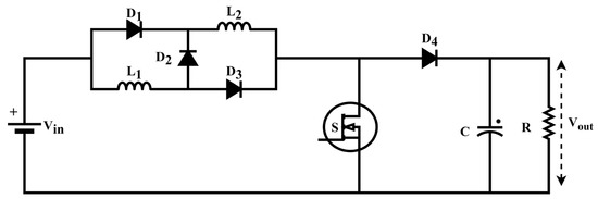
Figure 1.
Existing SI-based QZS step-up converter topology.
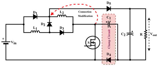
Figure 2.
Suggested SI-based MQZS step-up converter structure.
As indicated in Figure 2, the converter is different from the traditional QZS converter in two ways. Firstly, the connection of the output diode, D5, is changed to the junction point of the diode, D1, D2, and L2 (as indicated with red color arrow mark), which improves the voltage gain. Secondly, the clamping network that contains one capacitor, C1, and one diode, D4, is added (as indicated in the pink color box line), reducing the stress on the MOSFET switch. The following hypotheses are formulated before beginning the circuit analysis.
- The selected power semiconductors are ideal
- The proposed converter is working in the mode of continuous conduction
- Pulse-width modulation is the control approach utilized by switch S
The converter operation is divided into two modes. The theoretical waveform is illustrated in Figure 3. The current path during the two modes is illustrated in Figure 4.
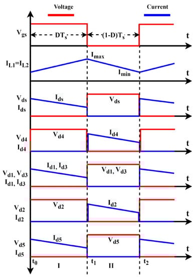
Figure 3.
Theoretical waveforms of the MQZS step-up converter.
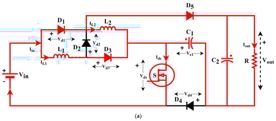
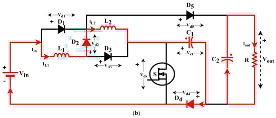
Figure 4.
Operating modes of the MQZS; (a) Mode−a; (b) Mode−b.
Mode-a (t0 − t1): Mode-a starts when the MOSFET device, S, is turn-on. The current path is illustrated in Figure 4a. During this mode, the inductors, L1 and L2, charge over the diodes, D3 and D1. The diode, D5, is forward biased due to its higher potential and distributes the required energy to the load. In addition, the C1 is getting charged through the load and the diode, D5. The diodes D2 and D4 are reverse-biased due to their lower potentials. The mode ends when S is switched off at t = t1. Throughout this duration, the output capacitor, C2, stores the energy.
Mode-b (t1 − t2): When the S is switched off, mode-b starts at t = t1. The current path is illustrated in Figure 4b. The diodes D1, D3, and D5 are turned off due to their lower potential, and the diodes D4 and D2 are forward biased due to their higher potential points. During this mode, both the inductors start discharging the energy through the diode D2, the diode D4 and the clamp capacitor C1. Thus, the MOSFET voltage stress is condensed by the C1 and the diode, D4. The output capacitor delivers the energy required by the load during mode-b. When the switch, S, is switched on, this mode is terminated at t = t2.
3. Steady-State Analysis and Parameter Selection of the Suggested MQZS Converter
3.1. Analysis during Steady-State
The theoretical discussion of the suggested converter is presented in this chapter for CCM operation only. During the first mode, the diode D1 and the capacitor C1 are coupled in series with the source to provide the required energy to the load over the MOSFET switch. Kirchhoff’s voltage law (KVL) is applied to find the expressions for the inductor voltages, and and are written as follows.
The proposed MQZS converter output voltage is found using the following expression during mode−a.
During the second mode, the diode D4 provides a path for the discharging current of the inductors to flow through the capacitor, C1. Again, by applying KVL, the following equations are derived.
The average voltage of the inductor is equivalent to zero as per the volt–second balance theory during steady-state conditions. Therefore, the voltage across the capacitor, , is written as follows.
The duty ratio of the MOSFET device is defined as D and is equal to Ton/Ts, where Ts denotes the total switching duration of the switch, and Ton is the conduction period of the switch. Therefore, the diode voltage stresses, and , are presented as follows.
Substitute Equations (4) and (5) in Equation (2) to derive the proposed converter output voltage equation, Vout, and is given as follows.
Therefore, the theoretical voltage gain, M, of the proposed MZS converter is written in Equation (7).
The voltage across the MOSFET switch, Vds, and the diode, , is derived as follows.
The voltage across the diodes and is derived as follows.
3.2. Parameter Selection
The average inductor current, and , is calculated using the following equation.
In general, the expression for the individual inductance, L1 or L2 is written as per Equation (12), and the actual expression for finding the minimum value of the inductance, L1,min, or L2,min, is written as follows: assuming 40% inductor current ripple.
where R denotes the load resistance, fs is MOSFET switching frequency, and %X is the inductor current ripple in percentage. The capacitor, C1, value is chosen as per the following equation, in which %x represents the voltage ripple in percentage.
The value of the output capacitor is chosen as per the following equation, in which %x represents the voltage ripple in percentage.
4. Simulation Results
The electrical specification and various variables of the proposed MQZS converter are recorded in Table 1. The simulation was performed using PLECS standalone software installed in a laptop with a 4.44 GHz clock frequency and 16 GB RAM. The same has been included in the revised version. The performance of the MQZS converter is validated using the specifications listed in Table 1.

Table 1.
Ratings of the MQZS converter.
As discussed earlier, the converter is simulated with the input voltage at 30 V and a constant load at 100 Ω (400 W). The MOSFET duty cycle is adjusted to 70% to reach the required voltage gain of 6.67. First, the simulation waveforms for the Vds and , and the current stress of S and D4 are demonstrated in Figure 5.
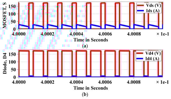
Figure 5.
Current and voltage stress waveforms: (a) MOSFET switch, S; (b) Diode, D4.
From Figure 5, the MOSFET switch voltage stress and D4 are noticed as 170 V and are equal to the theoretical discussion as per Equation (8). To prove the converter operation in CCM, the current wave shape of inductors is seen in Figure 6. It is seen from Figure 6 that the converter is operating at CCM (current never reaches zero at any instant). The inductor’s average current is equivalent to 6.95 A.
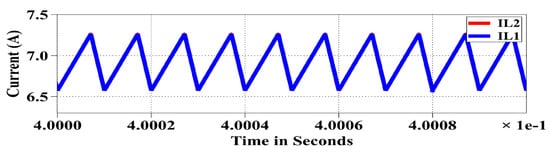
Figure 6.
Inductor current waveforms of the converter.
The current and voltage stresses of the diodes, D1–D3 and D5 are demonstrated in Figure 7. From Figure 7a,b, the diode voltage stress, and are equivalent to 70 V. The diode voltages, , are equal to 30 V, as realized in Figure 7c. The voltage across the diode, , is equal to 100 V, as realized in Figure 7d. All the voltages are equal to the theoretical values as per Equations (5), (9) and (10).
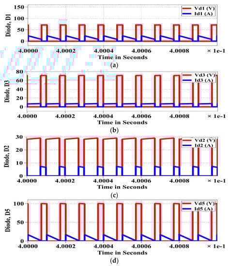
Figure 7.
Current and voltage stress waveform: (a) Diode, D1; (b) Diode, D3; (c) Diode, D2; (d) Diode, D5.
Figure 8 depicts the waveforms for the capacitor, the source voltage, and the input current. From Figure 8a, it is noticed that the capacitor voltage is equal to 170 V as per Equation (4). The main benefit of the MQZS step-up converter is a continuous input current. The input current is continuous, as seen in Figure 8b.
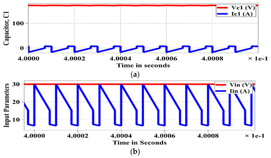
Figure 8.
Current and voltage stress waveforms: (a) Capacitor, C1; (b) Input source.
Figure 9 illustrates the output voltage and current waveforms of the MQZS converter. It is noticed from Figure 9a that the load voltage is equal to 200 V with the output current of 2 A, as seen in Figure 9b.
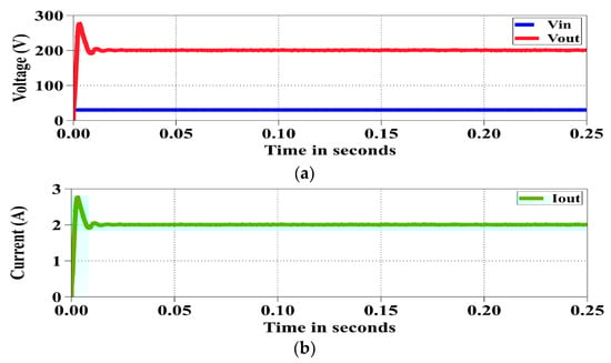
Figure 9.
Current and voltage waveforms: (a) Output voltage; (b) Output current.
From the above simulation results, the MQZS converter performs better according to theoretical analysis, as noted. In addition, the proposed MQZS DC-DC converter accomplishes better performance than the traditional QZS converter.
5. Hardware Results
The experimental prototype of the suggested MQZS converter with a 400 W rating is made and verified in the research laboratory environment. The electrical specification of the MQZS converter is recorded in Table 1, and the devices required for the prototype are recorded in Table 2.
Table 2.
Required Devices of the MQZS Converter.
The duty cycle of the MOSFET device is tuned to 70% to obtain the essential voltage gain from the proposed converter. The MQZS converter’s current and voltage waveforms are seen in Figure 10 for Vin = 30 V and Vout = 200 V. The switching frequency of the MOSFET switch is 100 kHz. The source voltage and input current waveform are illustrated in Figure 10a. As seen in Figure 10a, the input voltage is 30 V, and the average input current is 14.2 A. It is also noted that the source current is continuous. The voltage across L1 and L2 is depicted in Figure 10b. The average current of both L1 and L2 is equal to 7.08 A, and the CCM operation of the converter was also observed. In addition, the output voltage and output current of the MQZS converter is depicted in Figure 10c.
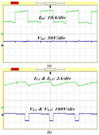
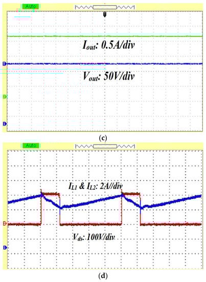
Figure 10.
Experimental waveforms of the MQZS converter.
As seen in Figure 10c, the output current of the MQZS converter is equal to 2.1 A, and the output voltage of the converter is equivalent to 198.2 V. The MOSFET switch voltage stress is less than 200 V as per Equation (8), and it has been seen in Figure 10d. In addition, the continuous conduction mode of the converter is confirmed, as seen in Figure 10d. The voltage waveforms, such as , , and , are depicted in Figure 11.
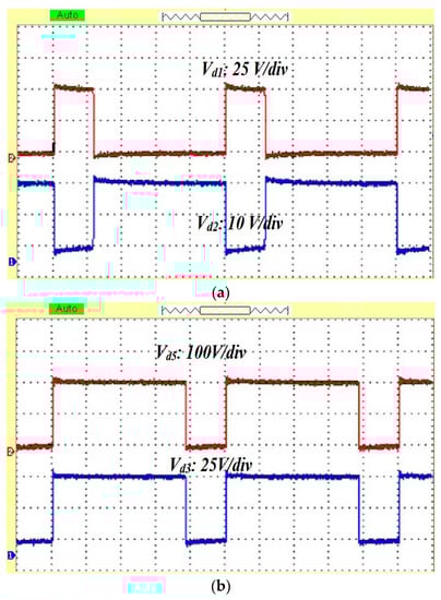
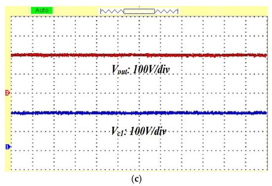
Figure 11.
Various waveforms: (a) and ; (b) and ; (c) and Vout.
As seen in Figure 11a, the voltage of the diode D1 is less than 70 V, and the voltage across the diode D2 is less than 30 V, and these voltages are the same as per Equation (5) and Equation (9). Figure 11b displays the voltage waveforms of and , and the values of these voltages are equal to 58 and 200 V, respectively, as per Equation (5) and Equation (10). The capacitor voltage, , waveform is illustrated in Figure 11c and equals less than 170 V.
The proportional-integral (PI) controller verifies the dynamic response of the MQZS converter. The output voltage of the converter is sensed using the voltage sensor, LEM LV 25-P, and fed to the comparator to compare the actual voltage and converter’s reference voltage. The controller gain of the PI controller is chosen as Ki = 0.01 and Kp = 0.5 based on the trial-and-error method. The voltage control can control the output voltage at 200 V, even if the input voltage is continuously changed, as shown in Figure 12, from 35 to 25 V. The source voltage is retained as 30 V at the beginning, and at t = 5 s, the source voltage is changed to 35 V and changed to 25 V in 10 s again. The proposed converter’s dynamic output voltage waveform for the change in input voltage is seen in Figure 12. As seen in Figure 12, the MQZS converter maintains a constant output voltage, regardless of the input voltage change.
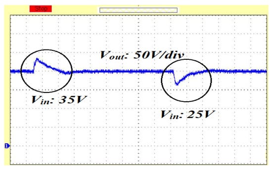
Figure 12.
Dynamic response of the MQZS converter.
It is fair to compare the suggested converter with the conventional QZS converter. Therefore, the converter performance comparison in terms of the capacitor voltage, the output voltage, the switch voltage stress, and the input current with the traditional converter is listed in Table 3.
Table 3.
Performance comparison among QZS and MQZS converter at Vin = 30 V with same output voltage.
From Table 3, the switch voltage stress and capacitor voltage stress of the proposed converter are lesser than the traditional QZS converter for the same output voltage. The traditional converter can obtain the output voltage of 109.09 V at 57% of the duty cycle, whereas the proposed converter can obtain the same output voltage at 45% of the duty cycle. From these discussions, it is concluded that the performance of the proposed converter better than the traditional QZS converter in all aspects. Thus, the dimensions and cost of the suggested MQZS converter have been reduced mostly. Figure 13 displays the voltage gain characteristics of the MQZS converter and other similar converters in the literature. Besides, the MQZS converter voltage gain by considering the internal elements of various components is also demonstrated in Figure 13.
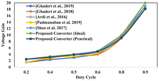
Figure 13.
Voltage gain characteristics of various converters [18,19,20,25,26].
Figure 13 shows that the voltage gain is reduced at a high duty cycle due to the influence of parasitic components of various devices. Therefore, it is not advisable to operate the converter at a high duty cycle, i.e., beyond 70% duty cycle. In addition, the high duty cycle also reduces the conversion efficiency due to high voltage drop across the parasitic elements and the conduction power losses. The efficiency curve assessment of the suggested MQZS converter with the other converter structures is illustrated in Figure 14. As seen in Figure 14, the effectiveness of the suggested MQZS converter is high due to a smaller number of components when related to the converters discussed in the literature. The maximum efficiency of the MQZS converter at 300 W is 94.2%, and the converter’s efficiency at full load is equivalent to 93.1%.
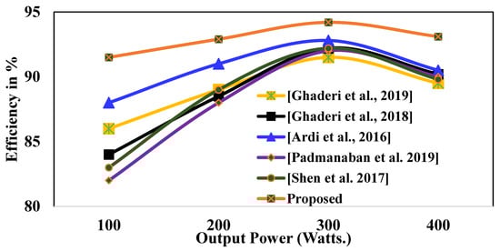
Figure 14.
Efficiency curve of different converters [18,19,20,25,26].
6. Conclusions
This paper comprehensively studied and analyzed the traditional QZS converter and modified the QZS dc-dc boost converter with one MOSFET switch. The proposed MQZS converter is an enhanced version of the traditional QZS converter, as it offers a high voltage gain, similar to the QZS converter. The prototype of the proposed MQZS dc-dc converter is made and experimented with in the laboratory environment. The experimental outcomes confirm the theoretical discussion and simulation results of the MQZS dc-dc converter. The operation, analysis, and parameter selection of the proposed MQZS converter were detailed in this paper. Moreover, the performance comparison is made with converters in previous works, and it is noted that the proposed MQZS converters offer high performance in the non-isolated converter category. The MQZS dc-dc converter can attain high output voltage gain with less voltage switch stress of the MOSFET, diodes, and capacitor. It also has benefits such as low cost and high-power density. Thus, the suggested MQZS converter is more appropriate for renewable energy systems that require a high output voltage from a low source voltage. In the future, the proposed converter can also be extended to various applications, such as electric vehicle power train systems, solar photovoltaic powered pumping systems, DC microgrid systems, etc.
Author Contributions
Conceptualization, M.P., R.S. and C.R.; methodology, M.P.; software, M.P., and R.S.; validation, M.P., P.J., C.K. and R.S.; formal analysis, M.P., C.R. and P.J.; investigation, M.P., T.R.S. and R.S.; resources, M.P., C.R. and C.K.; data curation, M.P., T.R.S. and R.S.; writing—original draft preparation, M.P. and R.S.; writing—review and editing, C.R., C.K., T.R.S. and P.J.; visualization, M.P.; supervision, M.P.; project administration, M.P. and P.J. All authors have read and agreed to the published version of the manuscript.
Funding
This research received no external funding.
Informed Consent Statement
Not applicable.
Data Availability Statement
Not applicable.
Acknowledgments
The authors would like to acknowledge the blind reviewers for their constructive comments to improve the paper. The authors would like to thank the management of Dayananda Sagar College of Engineering, Bengaluru, for providing the facility to experiment.
Conflicts of Interest
The authors declare no conflict of interest.
References
- Wu, G.; Ruan, X.; Ye, Z. Non-isolated high step-up DC-DC converter adopting auxiliary capacitor and coupled inductor. J. Mod. Power Syst. Clean Energy 2018, 6, 384–398. [Google Scholar] [CrossRef]
- Premkumar, M.; Kumar, C.; Sowmya, R. Analysis and implementation of high-performance DC-DC step-up converter for multilevel boost structure. Front. Energy Res. 2019, 7, 149. [Google Scholar] [CrossRef]
- Leon-Masich, A.; Valderrama-Blavi, H.; Bosque-Moncusí, J.; Martínez-Salamero, L. A High-Voltage SiC-Based Boost PFC for LED Applications. IEEE Trans. Power Electron. 2016, 31, 1633–1642. [Google Scholar] [CrossRef]
- Premkumar, M.; Kumar, C.; Anbarasan, A.; Sowmya, R. A novel non-isolated high step-up DC-DC boost converter using single switch for renewable energy systems. Electr. Eng. 2020, 102, 811–829. [Google Scholar] [CrossRef]
- Premkumar, M.; Sowmya, R.; Karthick, K. A dataset of the study on design parameters for the solar photovoltaic charge controller. Data Brief 2018, 21, 1954–1962. [Google Scholar] [CrossRef]
- Premkumar, M.; Sumithira, T.R. Design and implementation of new topology for solar PV based transformerless forward microinverter. J. Electr. Eng. Technol. 2019, 14, 145–155. [Google Scholar] [CrossRef]
- Forouzesh, M.; Siwakoti, Y.; Gorji, S.; Blaabjerg, F.; Lehman, B. Step-Up DC-DC Converters: A Comprehensive Review of Voltage-Boosting Techniques, Topologies, and Applications. IEEE Trans. Power Electron. 2017, 32, 9143–9178. [Google Scholar] [CrossRef]
- Richard, C.; McDonald, K.; St-Onge, X.; Saleh, S. A New Isolated DC-DC Converter for Discontinuous Input and Continuous Output. IEEE Trans. Ind. Appl. 2019, 55, 4215–4224. [Google Scholar] [CrossRef]
- Park, K.; Moon, G.; Youn, M. Non-isolated High Step-up Boost Converter Integrated with Sepic Converter. IEEE Trans. Power Electron. 2010, 25, 2266–2275. [Google Scholar] [CrossRef]
- Dwari, S.; Parsa, L. An Efficient High-Step-Up Interleaved DC-DC Converter with a Common Active Clamp. IEEE Trans. Power Electron. 2011, 26, 66–78. [Google Scholar] [CrossRef]
- Liu, H.; Li, F. Novel High Step-Up DC-DC Converter with an Active Coupled-Inductor Network for a Sustainable Energy System. IEEE Trans. Power Electron. 2015, 30, 6476–6482. [Google Scholar] [CrossRef]
- Dhananjaya, M.; Potnuru, D.; Manoharan, P.; Alhelou, H.H. Design and Implementation of Single-Input-Multi-Output DC-DC Converter Topology for Auxiliary Power Modules of Electric Vehicle. IEEE Access 2022, 10, 76975–76989. [Google Scholar] [CrossRef]
- Tang, Y.; Wang, T.; Fu, D. Multicell Switched-Inductor/Switched-Capacitor Combined Active-Network Converters. IEEE Trans. Power Electron. 2015, 30, 2063–2072. [Google Scholar] [CrossRef]
- Prabhala, V.; Fajri, P.; Gouribhatla, V.; Baddipadiga, B.; Ferdowsi, M. A DC-DC Converter with High Voltage Gain and Two Input Boost Stages. IEEE Trans. Power Electron. 2016, 31, 4206–4215. [Google Scholar] [CrossRef]
- Premkumar, M.; Sumithira, T.R. Design and implementation of new topology for non-isolated DC-DC microconverter with effective clamping circuit. J. Circuits Syst. Comput. 2019, 28, 1950082. [Google Scholar] [CrossRef]
- Abdel-Rahim, O.; Orabi, M.; Abdelkarim, E.; Ahmed, M.; Youssef, M.Z. Switched inductor boost converter for PV applications. In Proceedings of the Twenty-Seventh Annual IEEE Applied Power Electronics Conference and Exposition, Orlando, FL, USA, 5–9 February 2012; pp. 2100–2106. [Google Scholar]
- Tang, Y.; Xie, S.J.; Zhang, G.H.; Xu, Z.G. Improved Z-source inverter with reduced Z-source capacitor voltage stress and soft-start capability. IEEE Trans. Power Electron. 2009, 24, 409–415. [Google Scholar] [CrossRef]
- Ghaderi, D.; Bayrak, G. Performance Assessment of a High-Powered Boost Converter for Photovoltaic Residential Implementations. Elektron. Elektrotech. 2019, 25, 40–47. [Google Scholar] [CrossRef]
- Ghaderi, D.; Çelebi, M.; Minaz, M.R.; Tören, M. Efficiency improvement for a DC-DC quadratic power boost converter by applying a switch turn-off lossless snubber structure based on zero voltage switching. Elektron. Elektrotech. 2018, 24, 15–22. [Google Scholar] [CrossRef]
- Ardi, H.; Ajami, A.; Kardan, F.; Avilagh, S.N. Analysis and implementation of a nonisolated bidirectional DC-DC converter with high voltage gain. IEEE Trans. Ind. Electron. 2016, 63, 4878–4888. [Google Scholar]
- Piresa, V.F.; Foitoa, D.; Silvab, J.F. A single switch hybrid DC/DC converter with extended static gain for photovoltaic applications. Elect. Power Syst. Res. 2017, 146, 228–235. [Google Scholar] [CrossRef]
- Marzang, V.; Hosseini, S.H.; Rostami, N.; Alavi, P.; Mohseni, P.; Hashemzadeh, S.M. A high step-up non-isolated dc-dc converter with flexible voltage gain. IEEE Trans. Power Electron. 2020, 35, 10489–10500. [Google Scholar] [CrossRef]
- Lee, S.; Do, H. Quadratic boost DC-DC converter with high voltage gain and reduced voltage stresses. IEEE Trans. Power Electron. 2018, 34, 2397–2404. [Google Scholar] [CrossRef]
- Maroti, P.K.; Al-Ammari, R.; Bhaskar, M.S.; Meraj, M.; Iqbal, A.; Padmanaban, S.; Rhaman, S. New tri-switching state non-isolated high gain DC-DC boost converter for microgrid application. IET Power Electron. 2019, 12, 2741–2750. [Google Scholar] [CrossRef]
- Padmanaban, S.; Maroti, P.K.; Holm-Nielsen, J.B.; Blaabjerg, F.; Leonowicz, Z.; Yaramasu, V. Quazi Z-Source Single Stage High Step-Up DC-DC Converter for Grid-connected PV Application. In Proceedings of the International Conference on Environment and Electrical Engineering and IEEE Industrial and Commercial Power Systems Europe, Genova, Italy, 10–14 June 2019; pp. 1–6. [Google Scholar]
- Shen, H.; Zhang, B.; Qiu, D. Hybrid Z-Source Boost DC-DC Converters. IEEE Trans. Ind. Electron. 2017, 64, 310–319. [Google Scholar] [CrossRef]
Publisher’s Note: MDPI stays neutral with regard to jurisdictional claims in published maps and institutional affiliations. |
© 2022 by the authors. Licensee MDPI, Basel, Switzerland. This article is an open access article distributed under the terms and conditions of the Creative Commons Attribution (CC BY) license (https://creativecommons.org/licenses/by/4.0/).