Communication

A Novel Electronic Chip Detection Method Using Deep Neural Networks

1
National Research Base of Intelligent Manufacturing Service, Chongqing Technology and Business University, Chongqing 400067, China
2
Bio-Computing Research Center, Harbin Institute of Technology, Shenzhen 518055, China
3
Shenzhen Key Laboratory of Visual Object Detection and Recognition, Harbin Institute of Technology, Shenzhen 518055, China
4
School of Electrical and Electronic Engineering, University of Adelaide, Adelaide, SA 5005, Australia
5
Department of Electrical Electronics and Telecommunications Engineering, University of Cuenca, Cuenca 010105, Ecuador
6
School of Engineering and Sciences, Campus Guadalajara, Tecnologico de Monterrey, General Ramon Corona 2514, Zapopan CP 45138, Mexico
*
Author to whom correspondence should be addressed.
These authors contributed equally to this work.
Machines 2022, 10(5), 361; https://doi.org/10.3390/machines10050361
Submission received: 21 April 2022 / Accepted: 7 May 2022 / Published: 10 May 2022
(This article belongs to the Special Issue Feature Papers to Celebrate the First Impact Factor of Machines)

Abstract

:
Electronic chip detection is widely used in electronic industries. However, most existing detection methods cannot handle chip images with multiple classes of chips or complex backgrounds, which are common in real applications. To address these problems, a novel chip detection method that combines attentional feature fusion (AFF) and cosine nonlocal attention (CNLA), is proposed, and it consists of three parts: a feature extraction module, a region proposal module, and a detection module. The feature extraction module combines an AFF-embedded CNLA module and a pyramid feature module to extract features from chip images. The detection module enhances feature maps with a region intermediate feature map by spatial attentional block, fuses multiple feature maps with a multiscale region of the fusion block of interest, and classifies and regresses objects in images with two branches of fully connected layers. Experimental results on a medium-scale dataset comprising 367 images show that our proposed method achieved m A P 0.5 = 0.98745 and outperformed the benchmark method.

1. Introduction

Electronic chip assembly is a key link of electronic manufacturing, and its task is to place and solder chips onto printed circuit boards (PCBs). After electronic chip assembly, the chip and PCB are combined for electronic production. In this process, placement error is the distance between the real and ideal positions that causes functional defects in electronic products. With chip detection methods, electronic products with large placement errors can be found as early as possible. Machine vision techniques can also be used to detect chip position without damaging electronic products. Therefore, chip detection methods based on machine vision play an important role in electronic industries.
Our electronic chip detection method was designed to estimate the class and location of chips in a PCB. This is implemented by a electronic chip detection system that integrates various electronic parts. As shown in Figure 1, the detection system consists of four parts: PCB conveyer, image capture module (including camera, lens, and lighter), x y moving module (not shown in Figure 1 for simplicity), and an industrial PC. The PCB to be detected is first transferred to the center of the chip detection system by the conveyor; the image capture module is moved to several predefined positions and takes pictures of the PCB; lastly, these pictures are processed by an industrial PC to classify and locate chips. Three examples of PCB images are illustrated in Figure 2, and their characteristics are given as follows:
(1)
there are multiple chips in one picture;
(2)
the background of PCB image is complex, including pins, pads, flame retardant layer, and silk screen;
(3)
the size, color, and other characteristics of chips vary greatly.

2. Related Work

To classify and locate chips from images, there are many research achievements on electronic chip detections methods based on machine vision. Crispin [1] incorporated a normalized cross-correlation (NCC) template-matching approach that could reduce computational cost by constraining the search space, and optimize the search strategy of template positions using a genetic algorithm. A tree step algorithm for light-emitting diode (LED) chip localization was proposed by Zhong [2]. First, the positions of potential chips were extracted by applying a image segmentation and blob analyzation method; then, orientations of potential chips were predicted on the basis of dominant orientations; lastly, chips were precisely located using gradient orientation features according to the predicted positions and orientations. Gao [3] proposed a novel algorithm to inspect ball grid array (BGA) component defects: first, a grayscale image of solder balls was extracted with an adaptive thresholding algorithm with modified ( ϵ , δ ) -component segmentation; then, the ball array was generated with a line-based-clustering method; lastly, the precise position and orientation of BGA were estimated from the recognition results. The main cause of errors in chip detection was analyzed by applying a two-step calibration algorithm in Wang [4]. Zhong [5] proposed a three-step algorithm to exclude polycrystalline and fragmentary LED chips. First, blobs were obtained from an image with a simple but efficient image segmentation algorithm; second, abnormal blobs were excluded, and the position and orientation of a potential object were predicted on the basis of the pose of the minimal enclosing rectangle of each candidate blob; lastly, precise LED chips in the originally captured image were located on the basis of gradient orientation features. Bai [6] studied an online component positioning problem based on corner points that incorporated preprocessing, coarse positioning, and fine positioning stages. The preprocessing stage applied Harris corners and subpixel corner points that were extracted from images of real components. The coarse positioning step used distance and shape feature matching methods to compute correct correspondences between key points and Harris corner points. Lastly, the coarse and fine positioning problems were formulated as least-squares error problems.
With the development of deep-learning theory, object detection methods have recently achieved great success [7,8,9]. Object detection methods based on deep learning can generally be divided into two categories: one- and two-stage methods. One-stage object detection methods directly embed location and classification subnetworks into the font of a main backbone network. Typical one-stage object detection methods include YOLO [10,11,12], SSD [13], and DSSD [14]. Two-stage object detection methods introduce region proposal networks to predict candidate bounding boxes, and estimate class and location with multilayer fully connected networks from these bounding boxes. Typical two-stage object detection methods include R-CNN [15,16,17] and ThunderNet [18]. One-stage object detection methods are faster than two-stage object detection methods, and two-stage object detection methods are more precise than one-stage object detection methods.
Deep-learning-based detection methods come from training a multilayer convolutional neural network from training data; thus, neural network architectures learning features from training data is a research hotspot. Lin [19] designed a two-pathway architecture that contained a top–down and a down–top pathway to extract multiscale hierarchical feature maps. Qin [18] proposed a lightweight architecture to realize real-time object detection. To enrich feature representation, several blocks were introduced in that network, such as the context enhancement module (CEM) and spatial attention module (SAM). Liu [20] proposed a context embedding object detection network to detect concealed objects from millimeter wave images. In context embedding object detect networks, backbone features are attached to tree parallel branches with dilation sizes of 3, 6 and 12 to form the context embedding module and to incorporate surrounding information. Fang [21] fused the semantic object feature extraction module (Conv2dNet), the spatiotemporal feature extraction module (Conv3DNet) and the saliency feature-sharing module to generate the final saliency map for real-time video processing. Wang [22] combined dual-branch feature extraction and gradually refined the cross-fusion module in the network for camouflaged object detection. Gu [23] assembled an X-ray proposal network that applies data augmentation to enlarge input image datasets, and an X-ray discriminative network that fuses region of interest (ROI) feature maps from several levels for baggage inspection. A bidirectional attention feature pyramid network with cosine similarity was proposed for photovoltaic cell defect detection [24].
Table 1 shows the advantages of existing methods, which have two disadvantages: (1) they cannot detect multiple chips at the same time, and (2) cannot process chip images with a complex background. These drawbacks render them unsuitable for real applications. To solve these problems, we propose a novel chip detection method motivated by [18,23,25].

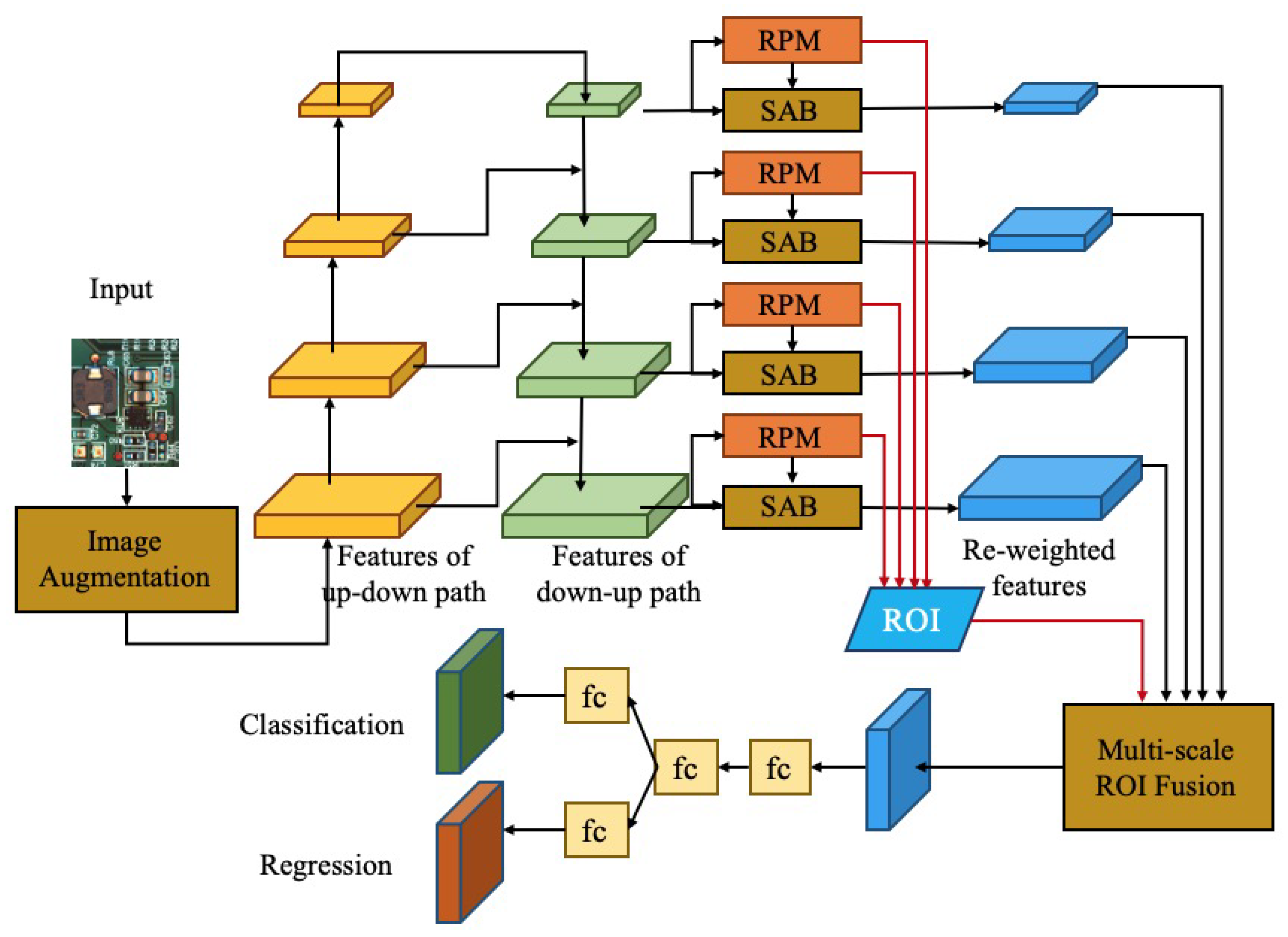
3. Proposed Methodology

In the electronic industry, the main aim of the proposed electronic chip detection method is to classify and locate chips in images. To overcome these challenges, a novel chip detection method is proposed in this work. Its methodology is composed of three steps: (1) AFF-embedded CNLA and pyramid-feature modules are combined to extract multiscale pyramid feature maps from chip images; (2) candidate bounding boxes are proposed in the region proposal module (RPM); (3) region intermediate feature maps are fused into enhanced feature maps from the spatial attentional block, and chip class and location are estimated by two branches of fully connected layers. The overall structure of the novel chip detection method is demonstrated in Figure 3.

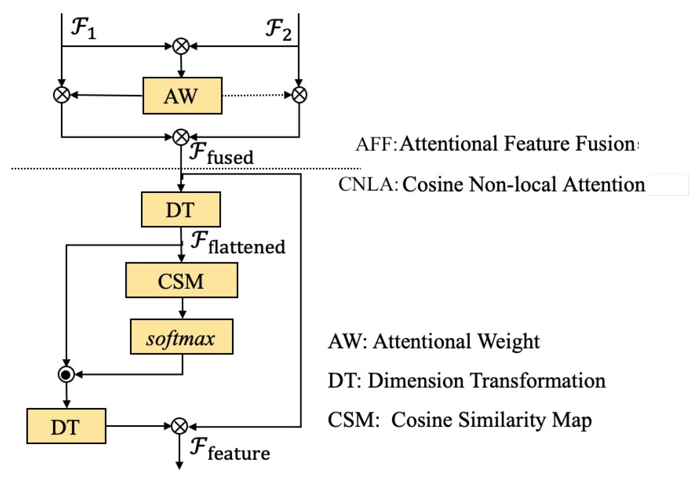
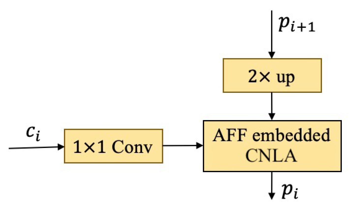
3.1. Feature Extraction Module

In traditional deep-learning-based object detection methods, a multilayer framework that contains a series of convolutional layers is utilized to extract high-level features from images. In the feature extraction framework, each layer takes the output of the lower layer as input and output features to the higher layer as input. The input of the lowest layer is the raw image, and the output of highest layer is used as the final feature of the detection module. To drop memory usage, convolutional layers in the feature extraction framework apply stride to reduce the feature map. This multilayer structure is able to learn feature extraction methods from large-scale training datasets, and its performance exceeds that of handcrafted feature extraction methods. Several research works [23,26] revealed that multilayer feature extraction cannot extract semantic and location information at the same time: semantic information exists in the upper layers but not in the lower layers, and the opposite for location information. As demonstrated in Figure 3, an improved feature pyramid framework was applied to extract image features in our work. Similar to feature pyramid networks (FPNs) [19], the feature extraction module (FEM) consists of two pathways: the bottom–up and up–bottom pathways.
In the proposed improved feature pyramid framework, the bottom–up pathway was designed to extract hierarchical features; hence, traditional multiple convolutional layer structure ResNet was employed, which is composed of 5 stages, and every layer of the same stage had the same output size. To save memory, the output of the first stage was ignored, and the output of remaining stages { C 2 , C 3 , C 4 , C 5 } was chosen to form the reference set.
Both semantic and location information is essential for object detection, but it is distributed in different layers in the bottom–up pathway. To combine this information, it is necessary to fuse features from different layers in the up–bottom pathway. In the highest layer of up–bottom pathway p 5 , the highest layer of bottom–up pathway c 5 was attached to a 1 × 1 convolutional layer. In other layers of up–bottom pathway { p i , i = 1 , . . . , 4 } , a building block was applied. The building block is illustrated in Figure 4: the feature from the same layer of down–up pathway c i was attached to a 1 × 1 convolutional layer, the feature from the higher layer of up–down pathway p i + 1 was attached to a 2 × up layer, and these two features were then fused into feature p i with the AFF-embedded CNLA block.
AFF-embedded CNLA block in Figure 4 demonstrated as in Figure 5, consisting of two parts: (top) AFF block; (bottom) CNLA block.
The AFF block [25] was designed to combine two input features F 1 and F 2 . To improve detection performance, global feature context (GFC) and local channel context (LCC) were both taken into account in the AFF block.
Considering feature F R C × H × W of C channels whose width and height were W and H, the GFC is defined as follows:
GFC ( F ) = BN ( W 2 · ReLU ( BN ( W 1 · g a p ( F ) ) ) ) ,
where W 1 and W 2 are two learnable parameters. BN in Equation (1) means batch normalization (BN) [27] that is proposed to address the internal covariate shift phenomenon in deep-learning networks. The internal covariate shift phenomenon is caused by the change in the input of each layer, increasing training epochs. In the BN layer, two parameters are introduced to scale and shift normalized values; then, normalization transformation can represent the identified transform. For input { x 1 . . . m } over a minibatch, the output of BN layer y i = BN ( x i ) is defined as follows:
μ B = 1 m i = 1 m x i ,
σ B 2 = 1 m i = 1 m ( x i μ B ) 2 ,
x ^ i = x i μ B σ B 2 + ϵ ,
y i = BN ( x i ) = γ x ^ i + β ,
where γ and β are two learnable parameters, and ϵ is the smallest positive value. ReLU in Equation (1) denotes rectified linear unit (ReLU) [28], and is an activation function for convolutional networks. The activation function can activate neural layers when the output reaches a predefined threshold, so it transforms input into the required output. ReLU is a nonlinear function that directly outputs the input value if it is positive; otherwise, it outputs zero. Mathematically, the ReLU is defined as follows:
y ( x ) = ReLU ( x ) = m a x ( 0 , x ) .
g a p ( F ) in Equation (1) is global average pooling of feature F :
g a p ( F ) = 1 H × W h = 1 H w = 1 W F [ : , h , w ] .
LCC of F is defined as below:
LCC ( F ) = BN ( P W C o n v 2 ( ReLU ( BN ( P W C o n v 1 ( F ) ) ) ) ) ,
where P W C o n v is pointwise convolution that uses a 1 × 1 kernel to aggregate channel context for each spatial position.
With GFC ( F ) and LCC ( F ) in Equations (1) and (8), the attentional weight ( AW ) of feature F in Figure 5 is defined as:
AW ( F ) = GFC ( F ) LCC ( F ) ,
where ⊕ is the broadcasting addition that adds scalars to higher-dimensional tensors. Lastly, as shown in the upper part of Figure 5, AFF is defined as:
F f u s e d = AFF ( F 1 , F 2 ) = AW ( F 1 F 2 ) F 1 + ( 1 AW ( F 1 F 2 ) ) F 2 ,
where ⊕ is the same broadcasting addition as that in Equation (9), and ⊗ is the element-wise multiplication that adds corresponding elements between tensors.
The second part of the AFF-embedded CNLA block is the CNLA block that is calculated from the output of the AFF block F f u s e d . The CNLA block is based on an improved nonlocal (NL) block [29]. In [29], the NL operation was defined as:
y i = 1 C ( x ) j f ( x i , x j ) g ( x j ) ,
where i is the position index of the output, and j enumerates all possible positions. x and y are input and output signals, respectively, with the same size. The f ( x i , x j ) function generates a scalar value between i and all j, and it is discussed in the next section. Function g ( x j ) generates a value for position i, and it can be considered in the form of linear embedding: g ( x j ) = W g x j , where W g is a learnable parameter. C ( x ) is the normalization coefficient. With the NL operation that is defined in Equation (11), the nonlocal block is defined as:
z i = W z y i + x i
where y i is defined in Equation (11), + x i denotes a residual connection, and W z is a learnable parameter.
The function of f ( x i , x j ) in Equation (11) has multiple potential options. In [24], cosine similarity was introduced as the f ( x i , x j ) function into the CNLA block:
f ( x i , x j ) = x i T x j x i x j .
Lastly, output y j of CNLA is defined as:
y j = j s i , j g ( x j ) + x j ,
where s i , j is the s o f t m a x operation performed on a row of the similarity map:
s i , j = exp f ( x i , x j ) j exp f ( x i , x j ) .

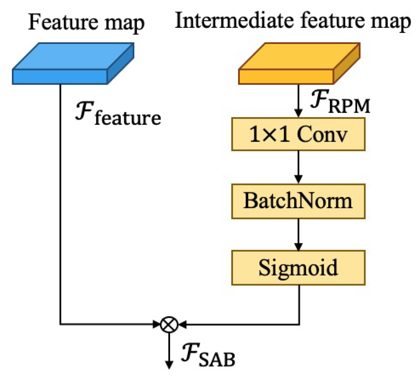
3.2. Region Proposal Module

Following FEM described in Section 3.1, the region proposal module (RPM) [17] is applied to estimate the rough location of objects. As shown in Figure 6, in the RPM, a feature map is attached to a 3 × 3 convolutional layer to generate the intermediate feature map (IFM) F I F M , and it was designed to collect information from neighboring regions of the feature map. Referring to [17], k reference boxes, namely, anchors, were predefined with different aspect ratios in every location of the intermediate feature map. To obtain the rough position of chips, F I F M is input into two 1 × 1 convolutional layers to obtain the scoring and regression layers. The scoring layer had k channels, and the regression layer had 4 k channels. For each location in the feature map, anchors with a higher score than the predefined thresholding were chosen as candidate ROIs, and accuracy could be further improved with the regression layer.

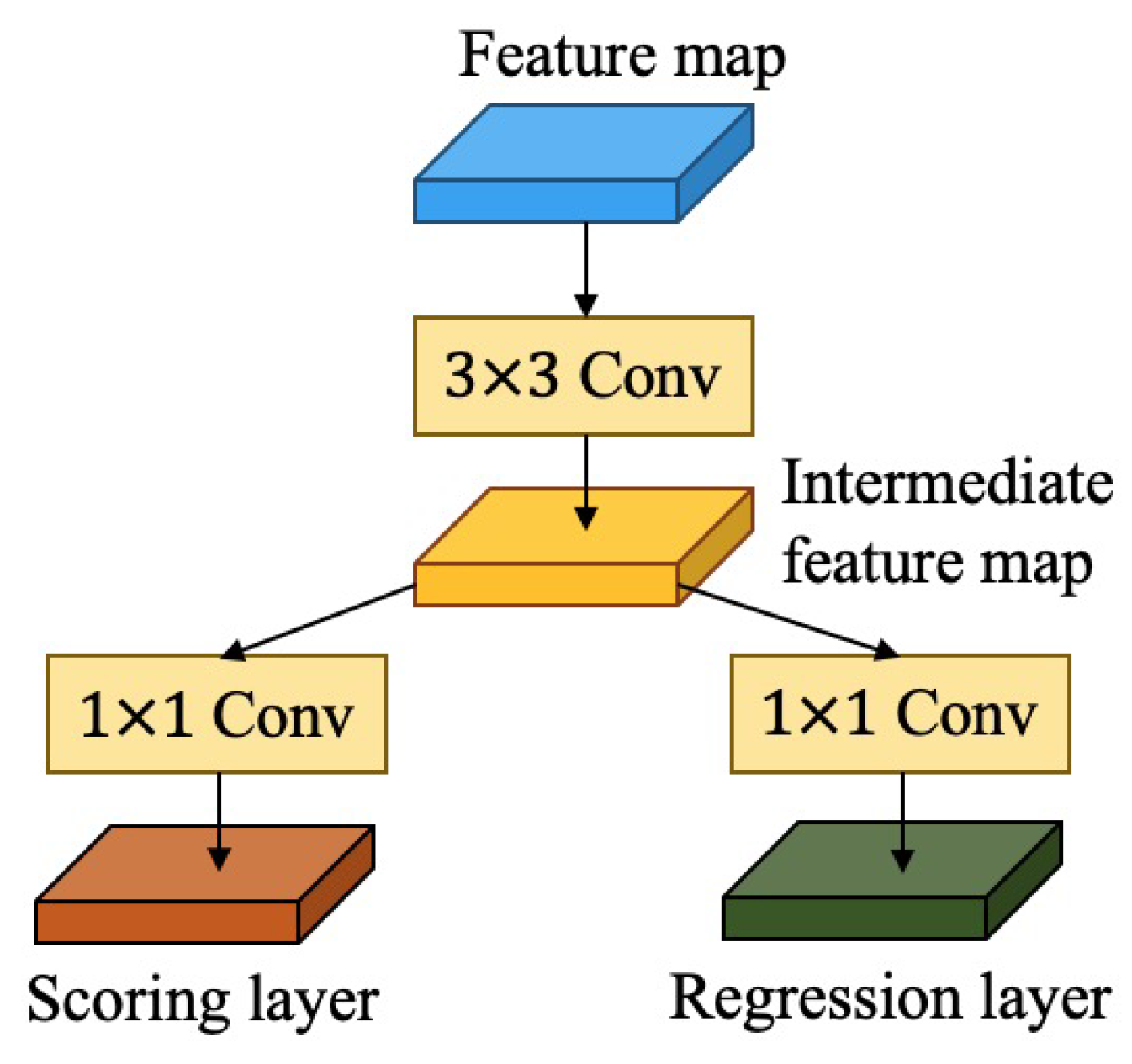
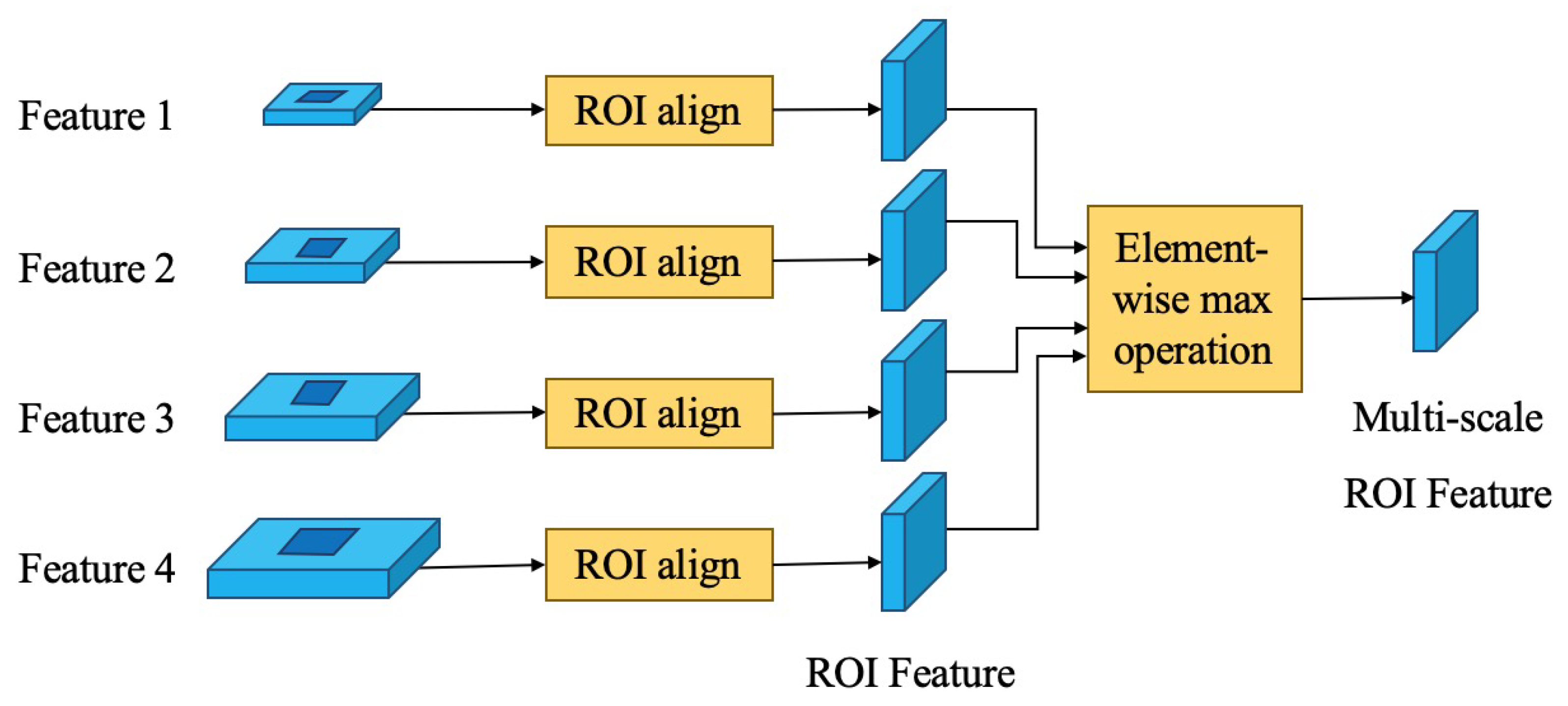
3.3. Detection Module

The detection module was designed to estimate the precise location and class of chips. Feature maps from FEM F f e a t u r e could be used in these tasks, but they could not provide feature distribution for the detection module. To solve this problem, the spatial attention block (SAB) [18] was applied to reweight F f e a t u r e with spatial dimensions from RPM. As shown in Figure 7, the intermediate feature map of FPM F I F M was attached to a 1 × 1 convolutional layer, followed by a BN layer and a sigmoid layer; then, it was multiplied by feature map F f e a t u r e to generate final result F S A M . The SAB is define as:
F S A B = F f e a t u r e · s i g m o i d ( BN ( F P R M ) ) ,
where BN denotes the BN layer described in Equation (5), and s i g m o i d is defined as:
s i g m o i d ( x ) = e x e x + 1 .
As shown in Figure 3, all of four outputs of the feature maps from FEM were attached to SAM to generate spatial attentional feature maps { s i , i [ 2 4 ] } . Although several measures were used in previous section, different information is contained in different feature maps. To combine these feature maps, as shown in Figure 8, the multiscale ROI fusion block [23] was introduced in our work. In the RPM section, ROIs were estimated in every feature map. Then, ROI information is input into the ROI align pooling (ROIAlign) layer [30] to extract ROI features that had the same size. In ROIAlign, ROIs are subdivided into spatial bins; the exact values of these bins are computed with bilinear interpolation and generate feature of ROI with aggregates. To obtain multiscale ROI features, these ROI features are fused with element-wise max operation.
Lastly, in order to detect the class and precise location of electronic chips, a fused feature is attached to a sequence of fully connected layers, followed by two branches of fully connect layers: one produces scores about k object classes, and the other generates four values for each K class that encodes refined bounding-box information.

3.4. Multitask Loss

Our detection network was assigned two tasks: classify and regress the bounding box that corresponded to two branches in the detection module. The loss function of our network is defined as follows [17]:
L ( { p i } , { t i } ) = 1 N c l s i L c l s ( p i , p i ) + λ 1 N r e g i p i L r e g ( t i , t i ) ,
where i is the index of anchors, and p i is the probability of the object in anchor i. The two terms are normalized by N c l s , N r e g , which are the minibatch size and the number of anchor locations, respectively, and they are weighted by a balancing parameter λ . L c l s ( p i , p i ) and L r e g ( t i , t i ) in Equation (18) are described as follows.
In Equation (18), p i is the ground truth of p i , defined as:
p i = 1 object is in the anchor i , 0 otherwise .
Classification loss L c l s is log loss over two classes (object versus not object).
L c l s ( p i , p i ) = log [ p i p i + ( 1 p i ) ( 1 p i ) ] .
t i is the reg vector with 4 elements that represents the predicted bounding box:
t x = x x a w a , t y = y y a h a , t w = w w a , t h = h h a .
t i is the ground truth of t i :
t x = x x a w a , t y = y y a h a , t w = w w a , t h = h h a ,
where x ,   y ,   w ,   and   h denote the central coordinates, width, and height of the predicted bounding box. To improve robustness, notation L r e g with L 1 smooth is defined as:
L r e g ( t i , t i ) = 0.5 ( t i t i ) 2 i f | t i t i | < 1 , | t i t i | 0.5 otherwise .
With loss function L defined in Equation (18), learnable parameters can be trained with the stochastic gradient descent method:
θ ( t + 1 ) = θ ( t ) γ L θ ,
where θ is one of learnable parameters, and γ is the learning rate.

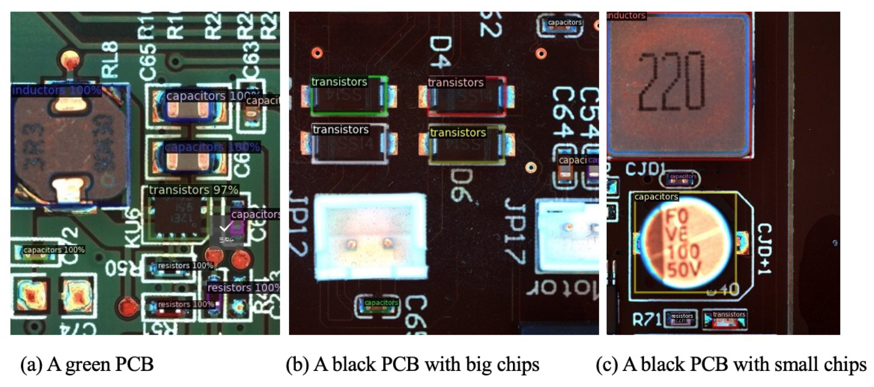
4. Experimental Results
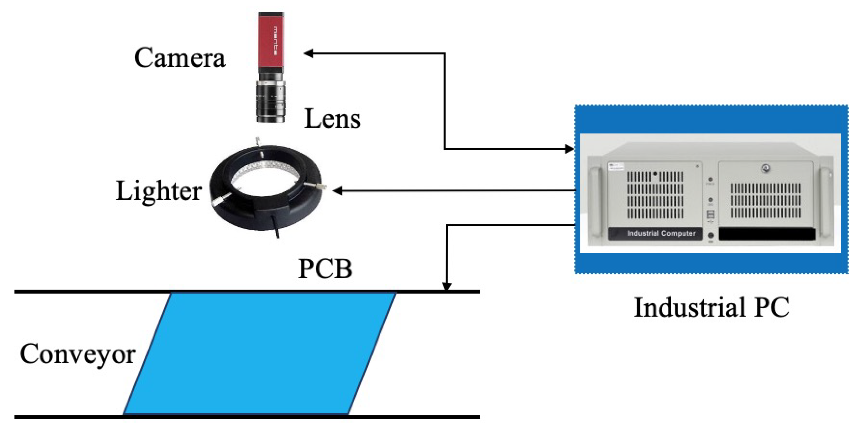
4.1. Dataset

In this section, the proposed chip detection method is evaluated on our chip image dataset. In the electronic industry, the appearance of PCBs and chips largely varies. So, it is impossible to generate a unified dataset that meets the requirements of all chip detection applications. To this end, chip detection application generally relies on small-scale datasets. This image dataset had 367 images, and was divided into two subsets: the training dataset contained 330 images, and the evaluation dataset contained 37 images. Images of the dataset were captured by the electronic chip detection system that is illustrated in Figure 1. On the basis of the image capture strategy, chip images were randomly cropped, and their width was between 300 and 700 pixels. Each image contained at least five chips belonging to at least two classes. Distribution of instances of the chip dataset is shown in Table 2.

4.2. Implement Details

The proposed chip detection method was evaluated on a workstation with an Intel Xeon (R) Gold 6278C CPU and a Nvidia Tesla V100 GPU. The network was implemented with Python programming language based on PyTorch [31] and its expansion pack Detectron2 [32]. The pretrained checkpoint of ResNet from Detectron2 was used to initialize the backbone of our method.
As discussed in Section 4.1, electronic chip detection methods are always trained with small-scale datasets and are prone to overfitting. To solve this problem, data augmentation was applied to our method. Through expanding the training dataset, data augmentation technology is able to improve generalization and robustness against changes in the input image, such as regarding image density, object position, and object orientation. In this paper, three augmentations are used:
(1)
random crop augmentation: cropping a region with random size from raw images;
(2)
random flip augmentation: randomly flipping the image;
(3)
small object augmentation [33]: copying small objects from the original position and pasting them to different positions.
To learn parameters for our method, a back-propagation-based optimization method is applied to minimize the loss defined in Equation (18), which is a function of weight parameters. First, the derivative of the loss function to each weight was calculated; then, a stochastic gradient descent method with momentum was applied to update weights in the direction of the fastest gradient decent until the maximal iteration. The previous momentum was used to accelerate the current gradient: update direction was defined by the previous update direction and the gradient of the current batch. In other words, if current and previous gradient directions are the same, update speed is higher; otherwise, update speed is lower. In our work, the learning rate was set to 0.0001, momentum was set to 0.9, and the maximal iteration was to 40,000.
In the RPM, the area of anchors for every pyramid feature maps was assigned to { 32 2 , 64 2 , 128 2 , 256 2 , 512 2 } , and the aspect ratio of all anchors was [ 1 3 , 1 2 , 1 , 2 , 3 ] . The maximal iteration was set to 8000, and the loss curve in training our method is shown in Figure 9. Experimental results of our method are demonstrated in Figure 10.

4.3. Evaluation Metrics

The performance of our method was established with the PASCAL criteria [34]. First, detection results were sorted by their confidence scores; then, the IoU was calculated for these results:
I o U = D e t e c t i o n R e s u l t G r o u n d T r u t h D e t e c t i o n R e s u l t G r o u n d T r u t h ,
where D e t e c t i o n R e s u l t is the bounding box of the detection result, and G r o u n d T r u t h is the annotation box. Then, l i t is defined as:
l i t = 1 a i > t 0 o t h e r w i s e
where a i is the IoU of i-th detection result, and t is the threshold. Precision p and recall r are defined as follows:
p i t = t p i t t p i t + f p i t r i t = t p i t n p t
where n p t is number of positive samples, and t p i t and f p i t are true positive and false positive, respectively:
t p i t = t p i 1 t + l i t f p i t = t p i 1 t + 1 l i t
On the basis of the area under precision recall curve, the A P was calculated as follows:
A P t = i n p p i Δ r .
The final m A P was calculated with the average value of A P for N classes:
m A P t = 1 N j = 1 N A P i t .
On the basis of m A P defined above, alternative criteria m A P c o c o were calculated by the average value of A P with t = 0.05:0.05:0.95 [35,36].

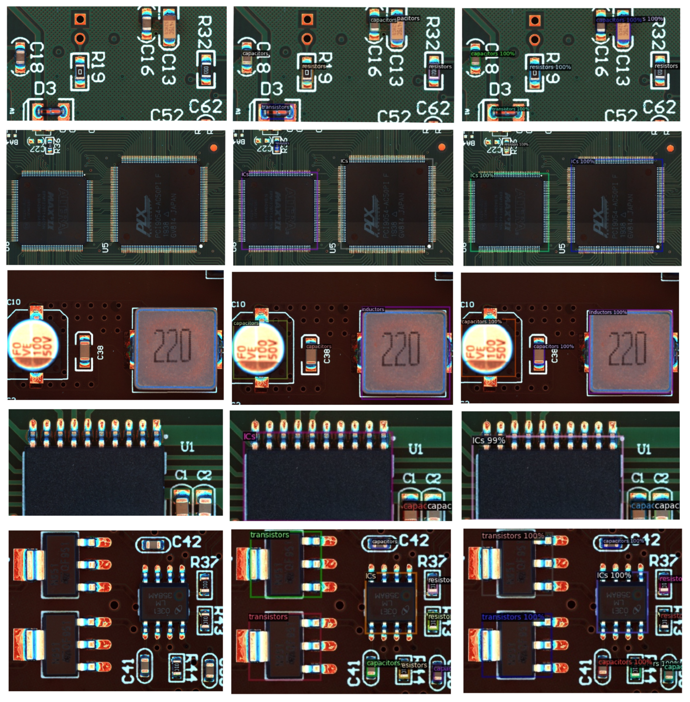
4.4. Evaluation Results

Table 3 shows the accuracy gap between our method and the faster R-CNN method, and Table 4 shows the difference between these two methods by category. As shown in Table 3, our method achieved promising results, outperformomg benchmark method R-CNN.
As shown in Table 3, the results of m A P 0.5 and m A P 0.75 in our method were 0.98745 and 0.95142 , respectively, while m A P C O C O was only 0.81130 . According to the definitions, m A P 0.5 evaluates detection results with the IoU threshold between bounding boxes of the detection results and ground truth, and this was equal to 50 % . m A P 0.75 evaluates detection results with a threshold equal to 75 % ; and m A P C O C O combines the IoU threshold from 50 % to 95 % in intervals of 5 % , that is, the requirement for IoU is higher. Therefore, our method could roughly detect electronic chips from the image, but, as shown in Figure 10, there was a certain error in the central coordinates and the size area. Hence, the accuracy of the bounding box could be further improved.
As shown in Table 4, the m A P C O C O the results of our method in detecting capacitors, transistors, ICs, and inductors were 0.80324 , 0.77550 , 0.88759 and 0.86782 , respectively, which ertr lower in detection resistors than those in the faster R-CNN method. According to our analysis, this result was because the surface of the resistors had text indicating the resistance value, so their surface texture was relatively complex. Compared with the faster R-CNN method, due to the extraction of more object features, our method was prone to overfitting when the amount of data was not large enough. Therefore, it is necessary to improve the accuracy of our method in detecting complex objects with a small amount of training data.

5. Conclusions

This paper proposed a novel electronic chip detection method that was trained with a small-scale chip dataset. Three aspects distinguish our work from previous works: first, our method was designed to detection chips that belong to different classes in complex backgrounds; second, AFF-embedded CNLA module and pyramid feature module were combined to extract features from chip images; third, pyramid feature maps were enhanced with the region intermediate feature map to classify and locate chips. The experiment showed that our work outperformed a landmark method. There are two challenges for our work: (1) the accuracy of the bounding box needs to be further improved; (2) the detection accuracy of objects with complex textures needs to be further improved. We will focus on improving the precision of the bounding boxes of electronic chips and the performance of the few-shot electronic chip detection method.

Author Contributions

Conceptualization, H.Z. and H.S.; data curation, H.S.; formal analysis, H.S.; funding acquisition, H.Z.; methodology, H.S.; project administration, H.S.; resources, H.S.; software, H.S.; supervision, P.S.; validation, P.S.; visualization, P.S.; writing—original draft, H.Z.; writing—review and editing, H.Z. and L.I.M. All authors have read and agreed to the published version of the manuscript.

Funding

This work was supported by the National Natural Science Foundation of China (62003062), the Science and Technology Research Project of Chongqing Municipal Education Commission (KJZD-M201900801 and KJQN201900831), the Chonqqing Natural Science Foundation (cstc2020jcyj-msxmX0077), the High-Level Talents Research Project of CTBU (1953013, 1956030, ZDPTTD201918), MOST Science and Technology Partnership Program (KY201802006), and the Open Fund Project of Chongqing Key Laboratory of Manufacturing Equipment Mechanism Design and Control (1556031).

Institutional Review Board Statement

Not applicable.

Informed Consent Statement

Not applicable.

Data Availability Statement

The source codes and datasets used to support the findings of this study are available from the corresponding author upon request via email: [email protected].

Conflicts of Interest

The authors declare no conflict of interest.

Abbreviations

The following abbreviations are used in this manuscript:
BGABall Grid Array
ROIRegion of Interest
PCBPrinted Circuit Board
NCCNormalized Cross Correlation
LEDLight-Emitting Diode
CEMContext Enhancement Module
SAMSpatial Attention Module
RPMRegion Proposal Module
FPNFeature Pyramid Network
FEMFeature Extraction Module
AFFAttentional Feature Fusion
CNLACosine Non-Local Attention
ReLURectified Linear Unit
SABSpatial Attention Block
IoUIntersection over Union

References

  1. Crispin, A.; Rankov, V. Automated inspection of PCB components using a genetic algorithm template-matching approach. Int. J. Adv. Manuf. Technol. 2007, 35, 293–300. [Google Scholar] [CrossRef] [Green Version]
  2. Zhong, F.; He, S.; Yi, J. A fast template matching method for LED chip Localization. MATEC Web Conf. 2015, 34, 04002. [Google Scholar] [CrossRef] [Green Version]
  3. Gao, H.; Jin, W.; Yang, X.; Kaynak, O. A line-based-clustering approach for ball grid array component inspection in surface-mount technology. IEEE Trans. Ind. Electron. 2016, 64, 3030–3038. [Google Scholar] [CrossRef]
  4. Wang, Z.; Gong, S.; Li, D.; Lu, H. Error analysis and improved calibration algorithm for LED chip localization system based on visual feedback. Int. J. Adv. Manuf. Technol. 2017, 92, 3197–3206. [Google Scholar] [CrossRef]
  5. Zhong, F.; He, S.; Li, B. Blob analyzation-based template matching algorithm for LED chip localization. Int. J. Adv. Manuf. Technol. 2017, 93, 55–63. [Google Scholar] [CrossRef]
  6. Bai, L.; Yang, X.; Gao, H. Corner point-based coarse–fine method for surface-mount component positioning. IEEE Trans. Ind. Inform. 2017, 14, 877–886. [Google Scholar] [CrossRef]
  7. Noe, S.M.; Zin, T.T.; Tin, P.; Kobayashi, I. Automatic detection and tracking of mounting behavior in cattle using a deep learning-based instance segmentation model. Int. J. Innov. Comput. Inf. Control 2022, 18, 211–220. [Google Scholar]
  8. Naufal, G.R.; Kumala, R.; Martin, R.; Amani, I.T.A.; Budiharto, W. Deep learning-based face recognition system for attendance system. ICIC Express Lett. Part B Appl. 2021, 12, 193–199. [Google Scholar]
  9. Putra, E.P.; Michael, S.; Wingardi, T.O.; Tatulus, R.L.; Budiharto, W. Smart traffic light model using deep learning and computer vision. ICIC Express Lett. 2021, 15, 297–305. [Google Scholar]
  10. Redmon, J.; Divvala, S.; Girshick, R.; Farhadi, A. You only look once: Unified, real-time object detection. In Proceedings of the IEEE Conference on Computer Vision and Pattern Recognition, Las Vegas, NV, USA, 27–30 June 2016; pp. 779–788. [Google Scholar]
  11. Redmon, J.; Farhadi, A. YOLO9000: Better, faster, stronger. In Proceedings of the IEEE Conference on Computer Vision and Pattern Recognition, Honolulu, HI, USA, 21–26 July 2017; pp. 7263–7271. [Google Scholar]
  12. Redmon, J.; Farhadi, A. Yolov3: An incremental improvement. arXiv 2018, arXiv:1804.02767. [Google Scholar]
  13. Liu, W.; Anguelov, D.; Erhan, D.; Szegedy, C.; Reed, S.; Fu, C.Y.; Berg, A.C. Ssd: Single shot multibox detector. In Proceedings of the European Conference on Computer Vision, Munich, Germany, 8–14 September 2016; pp. 21–37. [Google Scholar]
  14. Fu, C.Y.; Liu, W.; Ranga, A.; Tyagi, A.; Berg, A.C. Dssd: Deconvolutional single shot detector. arXiv 2017, arXiv:1701.06659. [Google Scholar]
  15. Girshick, R.; Donahue, J.; Darrell, T.; Malik, J. Rich feature hierarchies for accurate object detection and semantic segmentation. In Proceedings of the IEEE Conference on Computer Vision and Pattern Recognition, Columbus, OH, USA, 23–28 June 2014; pp. 580–587. [Google Scholar]
  16. Girshick, R. Fast R-CNN. In Proceedings of the IEEE International Conference on Computer Vision, Washington, DC, USA, 7–13 December 2015; pp. 1440–1448. [Google Scholar]
  17. Ren, S.; He, K.; Girshick, R.; Sun, J. Faster R-CNN: Towards real-time object detection with region proposal networks. IEEE Trans. Pattern Anal. Mach. Intell. 2017, 39, 1137–1149. [Google Scholar] [CrossRef] [PubMed] [Green Version]
  18. Qin, Z.; Li, Z.; Zhang, Z.; Bao, Y.; Yu, G.; Peng, Y.; Sun, J. ThunderNet: Towards real-time generic object detection on mobile devices. In Proceedings of the 2019 IEEE/CVF International Conference on Computer Vision (ICCV), Seoul, Korea, 27 October–2 November 2019; pp. 6717–6726. [Google Scholar]
  19. Lin, T.Y.; Dollár, P.; Girshick, R.; He, K.; Hariharan, B.; Belongie, S. Feature pyramid networks for object detection. In Proceedings of the 2017 IEEE Conference on Computer Vision and Pattern Recognition (CVPR), Honolulu, HI, USA, 21–26 July 2017; pp. 936–944. [Google Scholar]
  20. Liu, T.; Zhao, Y.; Wei, Y.; Zhao, Y.; Wei, S. Concealed object detection for activate millimeter wave image. IEEE Trans. Ind. Electron. 2019, 66, 9909–9917. [Google Scholar] [CrossRef]
  21. Fang, Y.; Ding, G.; Wen, W.; Yuan, F.; Yang, Y.; Fang, Z.; Lin, W. Salient object detection by spatiotemporal and semantic features in real-time video processing systems. IEEE Trans. Ind. Electron. 2020, 67, 9893–9903. [Google Scholar] [CrossRef]
  22. Wang, K.; Bi, H.; Zhang, Y.; Zhang, C.; Liu, Z.; Zheng, S. D2C-Net: A dual-branch, dual-guidance and cross-refine network for camouflaged object detection. IEEE Trans. Ind. Electron. 2022, 69, 5364–5374. [Google Scholar] [CrossRef]
  23. Gu, B.; Ge, R.; Chen, Y.; Luo, L.; Coatrieux, G. Automatic and robust object detection in X-Ray baggage inspection using deep convolutional neural networks. IEEE Trans. Ind. Electron. 2021, 68, 10248–10257. [Google Scholar] [CrossRef]
  24. Su, B.; Chen, H.; Zhou, Z. BAF-detector: An dfficient CNN-based detector for photovoltaic cell defect detection. IEEE Trans. Ind. Electron. 2022, 69, 3161–3171. [Google Scholar] [CrossRef]
  25. Dai, Y.; Gieseke, F.; Oehmcke, S.; Wu, Y.; Barnard, K. Attentional feature fusion. In Proceedings of the 2021 IEEE Winter Conference on Applications of Computer Vision (WACV), Waikoloa, HI, USA, 5–9 January 2021; pp. 3559–3568. [Google Scholar]
  26. Wang, P.; Chen, P.; Yuan, Y.; Liu, D.; Huang, Z.; Hou, X.; Cottrell, G. Understanding convolution for semantic segmentation. In Proceedings of the 2018 IEEE Winter Conference on Applications of Computer Vision (WACV), Lake Tahoe, NV, USA, 12–15 March 2018; pp. 1451–1460. [Google Scholar]
  27. Ioffe, S.; Szegedy, C. Batch normalization: Accelerating deep network training by reducing internal covariate shift. In Proceedings of the 32nd International Conference on Machine Learning (ICML), Lille, France, 6–11 July 2015; pp. 448–456. [Google Scholar]
  28. Nair, V.; Hinton, G.E. Rectified linear units improve restricted boltzmann machines. In Proceedings of the 27th International Conference on International Conference on Machine Learning (ICLM), Haifa, Israel, 21–24 June 2010; pp. 807–814. [Google Scholar]
  29. Wang, X.; Girshick, R.; Gupta, A.; He, K. Non-local neural networks. In Proceedings of the 2018 IEEE/CVF Conference on Computer Vision and Pattern Recognition, Salt Lake City, UT, USA, 18–23 June 2018; pp. 7794–7803. [Google Scholar]
  30. He, K.; Gkioxari, G.; Dollár, P.; Girshick, R. Mask R-CNN. IEEE Trans. Pattern Anal. Mach. Intell. 2020, 42, 386–397. [Google Scholar] [CrossRef]
  31. Paszke, A.; Gross, S.; Massa, F.; Lerer, A.; Bradbury, J.; Chanan, G.; Killeen, T.; Lin, Z.; Gimelshein, N.; Antiga, L.; et al. Pytorch: An imperative style, high-performance deep learning library. Adv. Neural Inf. Process. Syst. 2019, 32, 8026–8037. [Google Scholar]
  32. Wu, Y.; Kirillov, A.; Massa, F.; Lo, W.Y.; Girshick, R. Detectron2. 2019. Available online: https://github.com/facebookresearch/detectron2 (accessed on 11 October 2019).
  33. Kisantal, M.; Wojna, Z.; Murawski, J.; Naruniec, J.; Cho, K. Augmentation for small object detection. arXiv 2019, arXiv:1902.07296. [Google Scholar]
  34. Everingham, M.; Van Gool, L.; Williams, C.K.; Winn, J.; Zisserman, A. The pascal visual object classes (voc) challenge. Int. J. Comput. Vis. 2010, 88, 303–338. [Google Scholar] [CrossRef] [Green Version]
  35. Lin, T.Y.; Maire, M.; Belongie, S.; Hays, J.; Perona, P.; Ramanan, D.; Dollár, P.; Zitnick, C.L. Microsoft coco: Common objects in context. In Proceedings of the European Conference on Computer Vision, Zurich, Switzerland, 6–12 September 2014; pp. 740–755. [Google Scholar]
  36. Hosang, J.; Benenson, R.; Dollár, P.; Schiele, B. What makes for effective detection proposals? IEEE Trans. Pattern Anal. Mach. Intell. 2015, 38, 814–830. [Google Scholar] [CrossRef] [PubMed] [Green Version]
Figure 1. Electronic chip detection system.
Machines 10 00361 g001
Figure 2. PCB images.
Machines 10 00361 g002
Figure 3. Overall structure of our chip-detection neural network.
Machines 10 00361 g003
Figure 4. Building block to combine features from down–up and up–down pathways.
Machines 10 00361 g004
Figure 5. AFF-embedded CNLA block.
Machines 10 00361 g005
Figure 6. Region proposal module.
Machines 10 00361 g006
Figure 7. Spatial attention block.
Machines 10 00361 g007
Figure 8. Multiscale ROI fusion block.
Machines 10 00361 g008
Figure 9. Loss curve in training our method.
Machines 10 00361 g009
Figure 10. Experimental results of our method. (left) Raw image; (center) ground truth; (right) result of our method.
Machines 10 00361 g010
Table 1. Advantages of existing methods.
MethodReferenceAdvantages
Computer-vision-based methodsFTM [2]Fast template-matching method applied to LED chip localization.
LBC [3]Line-based clustering approach applied to BGA component localization.
VF [4]Main cause of errors in chip detection was analyzed.
BATM [5]Blob-analysis-based template matching method introduced into LED chip detection.
CPCF [6]Corner-point-based coarse fine method introduced into chip localization.
Deep-learning-based methodFPNFeature-pyramid-based feature extraction introduced into object detection.
Thunder Net [18]Context-enhancement and spatial-attention modules introduced into object detection.
COB [20]Context-embedding module introduced into concealed object detection form millimeter wave image.
SOD [21]Semantic object feature extraction module (Conv2dNet), spatiotemporal feature extraction module (Conv3DNet), and saliency feature-sharing module fused for real-time video object detection.
D2C-Net [22]Dual-branch feature extraction and gradually refined cross-fusion module fused for camouflaged object detection.
XRBI [23]X-ray proposal and X-ray discriminative networks assembled for baggage inspection.
PCDD [24]Bidirectional attention feature pyramid network introduced for photovoltaic-cell defect detection.
Table 2. Distribution of instances.
DatasetResistorCapacitorsTransistorICInductorTotal
Training665670307183541879
Evaluation706232168188
Table 3. m A P 0.5 , m A P 0.75 , and m A P c o c o on testing dataset.
mAP 0.5 mAP 0.75 mAP COCO
Faster R-CNN0.965700.916850.76109
Our method0.987450.951420.81130
Table 4. m A P c o c o on testing dataset and per category of bounding box m A P c o c o .
mAP COCO ResistorCapacitorsTransistorICInductor
Faster R-CNN0.761090.734930.773810.756770.813870.72608
Our method0.811300.722340.803240.775500.887590.86782
Publisher’s Note: MDPI stays neutral with regard to jurisdictional claims in published maps and institutional affiliations.

