Abstract
In this paper, the performance variations of SiC MOSFET-based voltage and current source inverters under gate oxide degradation are studied. It is confirmed that the turn-on and turn-off delays of SiC MOSFETs change significantly by high electric field stress, which accelerates the gate oxide degradation. Variations in the turn-on and turn-off delays of switching devices extend or reduce the duty error of voltage source inverters and current source inverters. The performance variations of the voltage and current source inverter due to the duty error changes caused by the gate oxide degradation are analyzed through simulations. As a result, the gate oxide degradation worsens the performance of the voltage source inverter. Furthermore, the negative gate oxide degradation, which lowers the threshold voltage, decreases the performance of the current source inverter.
1. Introduction
Along with gallium nitride (GaN) field effect transistor (FET), silicon carbide (SiC) metal-oxide-semiconductor field (MOSFET), a wide bandgap (WBG) device, is attracting attention as a next-generation power switching device due to its high efficiency and power density [1,2]. In particular, SiC MOSFET is increasingly used in systems close to human life, such as electric vehicles [3]. As a result, the reliability of SiC MOSFET is becoming more important.
A gate oxide degradation is a major aging phenomenon that affects the reliability of SiC MOSFET along with a package degradation [4]. The package degradation is caused by thermomechanical stress caused by temperature change [5]. If the package degradation continues, phenomena, such as bond wire crack and lift-off, occur, leading to a switching device failure [6,7]. Meanwhile, SiC MOSFET has a thin gate oxide layer, so electrons can be injected into the oxide layer by the Fowler–Nordheim tunneling current. Moreover, there are more interface trapped charges on the SiC/SiO2 interface than Si MOSFET [8,9]. In particular, the interface trapped charge reduces the effective channel-carrier mobility and changes the threshold voltage (Vth). The reduced effective channel-carrier mobility eventually increases the on-resistance (Ron) of the switch. The shift direction of the Vth is determined by the sum of the oxide trapped charge and the interface trapped charge. These charges are changed more significantly by the gate oxide degradation. An increase in Vth causes an increase in conduction losses. Moreover, a decrease in Vth increases the risk of the switch being turned on undesirably [10,11]. If the gate oxide degradation continues, the gate insulation is eventually destroyed, and the control ability of the gate to switch is lost [12].
The gate oxide degradation is accelerated under high electric field (HEF) stress or high-temperature stress [13]. HEF stress is divided into positive HEF (PHEF) stress applying a positive voltage to the gate, and negative HEF (NHEF) stress using a negative voltage. Characteristic changes during the gate oxide degradation of SiC MOSFETs have been studied through muchresearch [8,10,13,14,15,16,17], and Table 1 summarizes the previous research about the characteristics of SiC MOSFETs under gate oxide degradation. In Table 1, characteristics covered by the study were marked with an O, and properties not investigated by the analysis were marked with an X. Furthermore, the characteristics measured when the switching state is fixed are defined as stationary properties, and the properties measured when the switching state changes are defined as transient properties. The stationary properties are Vth, Ron, gate–drain capacitance (Cgd), gate–source capacitance (Cgs), and body diode forward voltage (Vsd). Moreover, the transient properties are Miller plateau voltage (Vm), Miller plateau time (Tm), gate charge time (Tgc), turn-on delay (Tdon), and turn-off delay (Tdoff).

Table 1.
Summary of previous research about characteristics of SIC MOSFETs under gate oxide degradation.
As shown in Table 1, previous studies dealt with the SiC MOSFET’s stationary properties under gate oxide degradation. However, research about transient characteristics of SiC MOSFET has not been conducted much. Especially, except for Tdon in [13], no studies on Tdon and Tdoff under gate oxide degradation were conducted in previous studies. Tdon and Tdoff can impact the performance of voltage and current source converters. The voltage source converter has a dead time to prevent a short circuit accident when one leg’s switches are turned on simultaneously [18]. The dead time causes a duty error in the voltage vector. In addition to the dead time, Tdon and Tdoff introduce duty errors. These duty errors change the output quality of the voltage source converter. Furthermore, an overlap time is required in the current source converter to prevent an overvoltage of the DC link inductor from occurring when all upper or lower switches are turned off simultaneously [19]. Like the voltage source converter, the overlap time, Tdon, and Tdoff generate the duty errors in the current vector, resulting in changes in the output quality of the current source converter. Therefore, studies on changes in Tdon and Tdoff under gate oxide degradation are necessary.
In this paper, the changes of Tdon and Tdoff of SiC MOSFET in the gate oxide degradation are examined. In addition, the effects of Tdon and Tdoff variations caused by the gate oxide degradation on the performance of voltage and current source inverters are studied.
The structure of this paper is as follows. Section 1 is the introduction. Section 2 analyzes the effects of Vth on Ron, Tdon, and Tdoff. Section 3 describes HEF stress to accelerate the gate oxide degradation. Section 4 compares Vth and Ron changes of SiC MOSFET under HEF stress with those of Si-based devices. Section 5 compares the changes in Tdon and Tdoff of SiC MOSFET under HEF stress with those of Si-based devices. In Section 6, the performance variations of voltage and current source inverters according to the duty error changes due to the gate oxide degradation are examined by the simulation. Section 7 is the conclusion.
2. Effects of Threshold Voltage Variation on On-Resistance, Turn-On Delay and Turn-Off Delay
2.1. Gate Oxide Degradation
Gate oxide degradation is aging occurring in the gate oxide layer. Furthermore, it is one of the major degradations of MOSFETs, like package degradation. As the gate oxide degradation progresses, there is a change in Vth, and this change can be explained by the oxide trapped charge and the interface trapped charge in the gate oxide layer. Figure 1 is a structure of the MOSFET and the gate oxide layer.
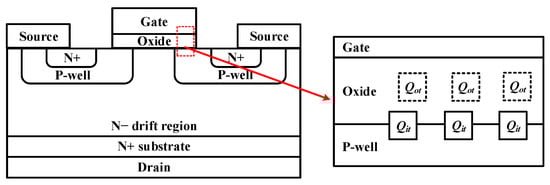
Figure 1.
Structure of the MOSFET and the gate oxide layer.
In Figure 1, Qot denotes the oxide trapped charge, and Qit means the interface trapped charge. By the gate oxide degradation, Qot is generated inside the oxide layer, and Qit is generated on the surface of the oxide layer. Vth can be expressed as (1) using Qot and Qit [20]:
In (1), Vth0 means Vth in a fresh condition where the gate oxide degradation does not proceed. Cox represents the gate oxide capacitance per unit area. Furthermore, q stands for the electric charge. Moreover, Nit and Not mean the interface trap density and the oxide trap density, respectively. When the gate oxide degradation proceeds, Qit and Qot are generated. Vth increases or decreases depending on which charge is more generated relatively. As seen from (1), when Qit occurs relatively significantly, Vth rises. On the other hand, when Qot is relatively large, Vth decreases. The gate oxide degradation is accelerated by HEF stress. In general, in PHEF stress where a positive voltage is applied to the gate voltage, Qit is generated significantly to increase Vth. Meanwhile, in NHEF stress where a negative voltage is applied to the gate voltage, Qot is generated relatively significantly, and Vth decreases.
2.2. On-Resistance Variation Caused by Threshold Voltage
Ron can be subdivided into several types of resistances as follows (2) [8]:
In (2), Rch is the channel resistance, RA is the accumulation resistance, RJFET is the JFET region resistance, Rd is the drift region resistance, and Rsub is the substrate resistance. In the case of SiC MOSFETs, among the five resistance types, Rch is the most dominant [8]. Rch can be expressed as (3) [8]:
In (3), Lch means the channel length, and Wch represents the channel width. In addition, μ and Vover represent the channel mobility and the overdrive voltage, respectively. Vover is expressed as the difference between the gate–source voltage (Vgs) and Vth. As seen from (3), the variation of Vover changes Rch. Therefore, when Vth changes, Rch also changes. When Vth increases, Vover decreases, and Rch increases. When Vth decreases, Vover increases, and Rch decreases. As a result, Ron increases when Vth increases, and Ron decreases when Vth decreases.
2.3. Turn-On Delay Variation Caused by Threshhold Voltage
A definition of Tdon is the time from when Vgs starts to rise to when the drain–source current (Ids) starts to increase [21]. Vth is related to Tdon because Vth is the voltage at which Ids starts flowing through the switch. Figure 2 shows Vgs and Ids waveforms when the switch is turned on.
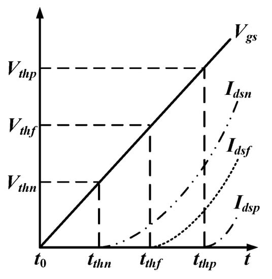
Figure 2.
Waveforms of Vgs and Ids in a turn-on state.
In Figure 2, t0 means the time when Vgs starts to increase to turn on the switch. In addition, tthf indicates the time when Ids in the fresh condition begin to rise. tthn and tthp denote a time at which Ids start to grow when Vth is negatively shifted and positively shifted, respectively. Vth and Ids in the fresh condition are expressed as Vthf and Idsf, respectively. Furthermore, Vth and Ids in the negative Vth shift are described as Vthn and Idsn, respectively. Moreover, Vth and Ids in the positive Vth shift are denoted as Vthp and Idsp, respectively. As shown in Figure 2, Ids starts to flow when Vgs becomes greater than Vth. Tdon of the fresh state, the negative Vth shift, and the positive Vth shift can be expressed by (4), respectively:
Tdonf, Tdonn, and Tdonp in (4) mean Tdon in fresh condition, negative Vth shift, and positive Vth shift, respectively. As shown in Figure 2, comparisons of Tdonf, Tdonn, and Tdonp are expressed as (5). Therefore, as Vth increases, Tdon increases:
2.4. Turn-Off Delay Caused by Threshold Voltage
A definition of Tdoff is the time from when Vgs starts to decrease to when the drain–source voltage (Vds) begins to grow [22]. The point at which Vds increases in the off transition is when Vgs enters Vm [22]. Therefore, the change in Tdoff can be explained by Vm. The relationship between Vm and Vth can be expressed by (6) [20]:
Partial differentiation of (6) with respect to Not and Nit gives the following (7) [20]:
From (7), it can be seen that an increase in Vth increases Vm and vice versa. Figure 3 shows the relationship between the change in Vm and Tdoff.
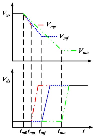
Figure 3.
Turn-off waveform of Vgs and Vds according to a variation of Vm.
In Figure 3, Vmp, Vmf, and Vmn mean Vm in positive Vth shift, fresh state, and negative Vth shift, respectively. In addition, tmp, tmf, and tmn indicate a time when Vds increases in positive Vth shift, fresh state, and negative Vth shift, respectively. tm0 is the point at which Vgs begins to decrease to turn off the switch. Figure 3 indicates that the time at which Vds increases is faster as Vm increases. Therefore, as Vm increases, Tdoff decreases and vice versa. Tdoff can be expressed as (8):
In (8), Tdoffp, Tdofff, and Tdoffn denote Tdoff in a positive Vth shift, fresh state, and negative Vth shift, respectively. The magnitudes of Tdoffp, Tdofff, and Tdoffn can be expressed as (9):
3. High Electric Field Stress
As shown in Figure 4, The HEF stress circuit was constructed to accelerate the gate oxide degradation. The fabricated circuit was configured to apply HEF stress to five devices simultaneously. The drain and source or collector and emitter of the switching device were shorted to be connected to the ground. A resistor of 200 Ω was inserted to alleviate the overshoot of the gate current when HEF stress was applied to the gate side [8]. HEF stress was applied for 3600 s at room temperature, and the switching devices were disconnected from the HEF stress circuit every 900 s to measure Vth, Ron, Tdon, and Tdoff of the switching devices. The gate bias value used for HEF stress should be the proper value for accelerating the gate oxide degradation and preventing the gate insulation destruction. For this, 50 V was used as the gate bias value in PHEF. In the case of NHEF, the gate bias value was set to −38 V. In this paper, characteristics, such as Vth, Ron, Tdon, and Tdoff, were compared by applying HEF stress under the same conditions to various Si-based devices as well as SiC MOSFET. The reason for this comparison is to confirm that SiC MOSFET is more susceptible to the gate oxide degradation compared to other Si-based devices. The Si-based devices used for comparison are Si IGBT, Si MOSFET, and Si IGBT with SiC diode. Information on the switching devices used for characteristic comparison is given in Table 2.
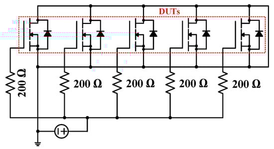
Figure 4.
HEF stress circuit.
Table 2.
Datasheet values of switching devices used in this paper.
The maximum gate voltages of Si IGBT, Si MOSFET, Si IGBT with SiC diode, and SiC MOSFET, as seen from the datasheet, are −30/+30 V, −30/+30 V, −20/+20 V, and −4/+22 V, respectively. Therefore, it can be inferred from the datasheet that the SiC MOSFET is most vulnerable to the large gate voltage. This paper experimentally checks a low-rated gate voltage of SiC MOSFET by applying the same voltage stress to four types of switching devices and examines a change of electrical characteristics caused by the gate oxide degradation.
4. Investigation of Threshold Voltage and On-Resistance under High Electric Field Stress
This paper investigated Vth and Ron according to HEF stress. The Vth and Ron measurement circuits were configured as shown in Figure 5.
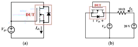
Figure 5.
Measurement circuits (a) Vth (b) Ron.
Figure 5 shows the case of Si MOSFET and SiC MOSFET. In the case of Si IGBT and Si IGBT with SiC diode, Vgs and Ids correspond to gate–emitter voltage (Vge) and collector–emitter current (Ice), respectively. Figure 5a shows the Vth measurement circuit.A device under test (DUT) is connected to measure Vth, as shown in Figure 5a.Then, the magnitude of Vgs is gradually raised from 0 V until Ids is 1 mA. Vgs, when Ids becomes 1 mA, is Vth [14]. As shown in Table 2, Ids (or Ice) used to measure Vth is very small for Si MOSFET and Si IGBT with SiC diode. These values are very small to measure with an oscilloscope. Therefore, Ids (or Ice) of 1 mA that can be measured with a small error is selected, and Vth is measured with 1 mA for all four devices.
Figure 5b represents the Ron measurement circuit. To measure Ron, the voltage used to measure Ron in the datasheet of each device is applied to Vgs. That is, Vgs for Ron measurement is 15 V for Si IGBT, 10 V for Si MOSFET, 15 V for Si IGBT with SiC diode, and 18 V for SiC MOSFET. Then, Ids and Vds when the switch is fully on are measured with an oscilloscope to eliminate the effect of parasitic components. Meanwhile, Ron varies with respect to the junction temperature.In order to reduce the variation caused by the junction temperature change, the temperature rise of the switch is minimized by applying Ids (about 2 A) which is much smaller than the rated value of the switch for a short time (about 40 ms). Ron is calculated using the measured Vds and Ids as (10):
Ron = Vds/Ids
The measured device characteristics are expressed as the rate of change concerning the initial value as (11):
Variation (%) = (Paging − Pfresh)/Pfresh·100
In (11), Paging represents a characteristic of the aging device. Moreover, Pfresh is a property of the fresh device. In Figure 6, the rules are established to distinguish the devices used in this paper.
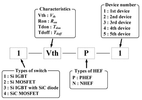
Figure 6.
Device naming rule in this paper.
Figure 6 shows the device naming rule used in this paper. A device’s name is divided into four parts. The first part indicates the type of switching device. As shown in Figure 6, a number is assigned to each switch type. The second part shows the measured device property. The third part is the type of HEF, and the last part means the device number. The example of Figure 6, 1-Vth-P-1, refers to the first switch among the five switches where PHEF stress is applied to the Si IGBT for the Vth measurement.
4.1. Threshold Voltage Variation under HEF Stress
Figure 7 is the Vth variations in PHEF stress according to the types of the switching device. In Figure 7, Si IGBT with SiC diode is named Si IGBT (hybrid). Figure 7a,b demonstrate that Vth of Si IGBT and Si MOSFET had little change under PHEF stress. For Si IGBT with SiC diode, as shown in Figure 7c, the average value of Vth increased by about 3% compared to the initial value. Figure 7d shows the Vth of SiC MOSFET according to PHEF stress time. In the case of SiC MOSFET, Vth rapidly increases after PHEF stress. After 900 s PHEF stress, the average variation of Vth exceeded 100%. Moreover, the average variation of Vth was 166% when PHEF stress was finished. Consequently, under PHEF stress, the SiC MOSFET’s Vth variation is more significant than Si-based devices. The Vth increment in SiC MOSFET indicates that Qit occurs relatively more than Qot.
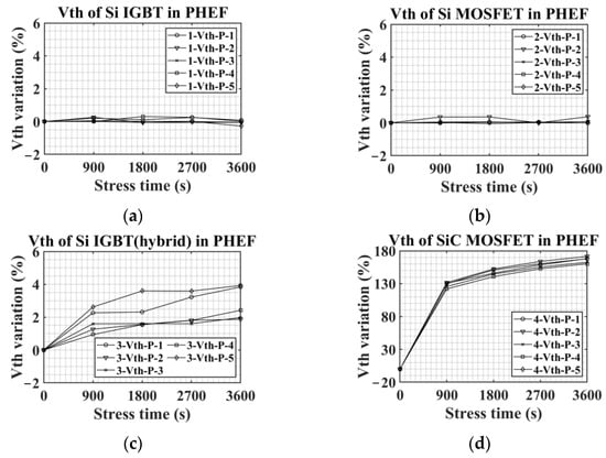
Figure 7.
Vth variations in PHEF stress: (a) Si IGBT, (b) Si MOSFET, (c) Si IGBT with SiC diode, and (d) SiC MOSFET.
A small level change in Vth without a noticeable increase or decrease trend can be regarded as a measurement error by the experimental equipment. Therefore, the Vth change of Si IGBT and Si MOSFET in Figure 7 can be considered as the measurement error. On the other hand, since Si IGBT with SiC diode and SiC MOSFET has a marked increase in Vth, even though considering the measurement error, Vth variations in Si IGBT with SiC diode and SiC MOSFET can be referred to as a permanent shift in Vth.
Figure 8 shows Vth variations in NHEF stress according to the types of the switching device. As demonstrated from Figure 8a, in the case of Si IGBT, there were few changes in Vth after NHEF stress. The average Vth variations of Si MOSFET and Si IGBT with SiC diode after 3600 s NHEF stress were −0.6% and −0.4%, respectively. For SiC MOSFET, the amount of Vth reduction was more significant than that of other types of switching devices. When the NHEP stress time was 900 s, averagely, Vth decreased by about 51% compared to the initial value, and when the stress was finished, Vth decreased by about 69%. The Vth reduction in SiC MOSFET means that Qot occurs more than Qit.
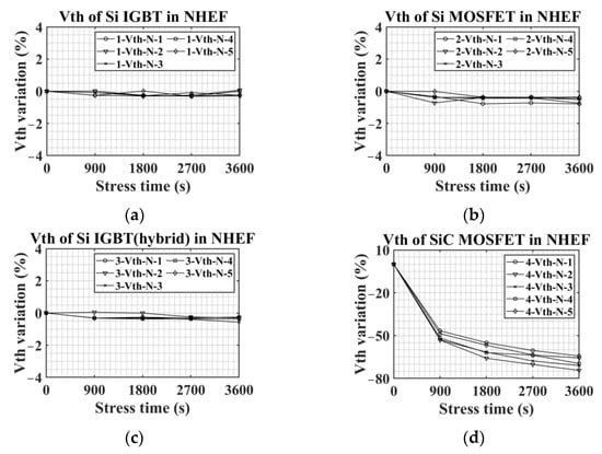
Figure 8.
Vth variations in NHEF stress: (a) Si IGBT, (b) Si MOSFET, (c) Si IGBT with SiC diode, and (d) SiC MOSFET.
Figure 8 indicates that, in NHEF stress, SiC MOSFET experiences considerable Vth reduction. This means that SiC MOSFETs have a greater risk of being switched on when they should be switched off than other types of switching devices. Therefore, SiC MOSFETs are more vulnerable to NHEF stress than Si-based devices.
4.2. On-Resistance Variation under HEF Stress
Figure 9 shows the changes of Ron in PHEF stress according to the switching device. For Si IGBT, shown in Figure 9a, Ron increased by about 1.3% compared to the initial value when the stress was finished. Furthermore, as shown in Figure 9b, the average Ron variation of Si MOSFET was about 0.3% after PHEF stress. For Si IGBT with SiC diode depicted in Figure 9c, four out of five DUTs showed little change, but 3-Ron-P-1 had a reduction tendency of Ron. From this, it can be seen that in the case of the Si-based device, the change in Ron according to PHEF stress is not significant. However, Ron of SiC MOSFET increased rapidly as PHEF stress progressed, as shown in Figure 9d. After the first 900 s of the stress, Ron increased by about 55% on average, and at the end of the stress, Ron rose to about 100% compared to the initial value. As shown in Figure 7d, Vth of SiC MOSFET in PHEF stress rose, resulting in the reduction of Vover in (3). As explained earlier, Ron of SiC MOSFET is greatly affected by Rch. Therefore, due to the decrement of Vover, Ron rose. Similar to the Vth trends in Figure 7, the rate of change of SiC MOSFET was the largest in Ron. These results indicate that the SiC MOSFET’s conduction loss can be larger than other Si-based devices in the positive gate oxide degradation that raises Vth.
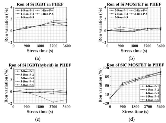
Figure 9.
Ron variations in PHEF stress: (a) Si IGBT, (b) Si MOSFET, (c) Si IGBT with SiC diode, and (d) SiC MOSFET.
Figure 10 shows the changes of Ron in NHEF stress according to the switching device. Figure 10a–c describe that Ron of Si IGBT, Si MOSFET, and Si IGBT with SiC diode had no trend according to NHEF stress. Ron of Si IGBT had the variation within about 6% depending on the stress. In the case of Si MOSFET, a device with an increase in Ron, a device with a decrease in Ron, and a device with few changes in Ron appear. Ron of Si IGBT (hybrid) had the slightest change according to NHEF stress. Meanwhile, Figure 10d demonstrates that SiC MOSFETs had a reduction trend of Ron according to NHEF stress. At the end of the stress, the variation in Ron of 4-Ron-N-1 was about −6%, and the variation in Ron of 4-Ron-N-5 was about 18%.
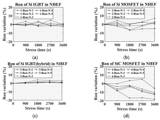
Figure 10.
Ron variations in NHEF stress: (a) Si IGBT, (b) Si MOSFET, (c) Si IGBT with SiC diode, and (d) SiC MOSFET.
The Ron reduction of SiC MOSFET in the NHEF stress can be explained by the Vth change. As shown in Figure 8d, Vth of SiC MOSFET decreases in NHEF stress. This Vth reduction raises Vover in (3). As a result, Ron decreases.
5. Turn-On and Turn-Off Delay under High Electric Field Stress
Figure 11 represents a double pulse test circuit (DPTC) used to measure Tdon and Tdoff. Figure 11 shows the DPTC used to measure the Tdon and Tdoff of the switching devices. A gate driver named SKHI22BR was used in this paper. The gate driver driving pulse in the DPTC was generated through a digital signal processor (DSP). The DSP used in this paper is TI TMS320F28335. Furthermore, UP-3005T was used for DC supply. Figure 11a is the circuit diagram for measuring Tdon and Tdoff. DUT is located at the bottom, as shown in Figure 11a. A large gate driver resistor was used to easily observe Tdon and Tdoff characteristics [17,21]. The gate driver resistor Rg for Tdon and Tdoff is 485 Ω.
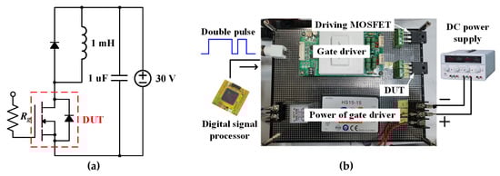
Figure 11.
DPTC (a) circuit diagram, and (b) picture of DPTC.
5.1. Turn-On Delay Variation under HEF Stress
Figure 12 shows some of the results of the Tdon experiment in PHEF stress. Tdon in the fresh state and Tdon after 3600 s of PHEF stress are displayed together. As shown in Figure 12, in the case of Si-based devices, the difference between before and after PHEF stress is not observed. However, as demonstrated from Figure 12d, Tdon of 4-Tdon-P-4, which is SiC MOSFET before the stress was about 232 ns, but Tdon measured after the stress was about 414.4 ns. Therefore, the Tdon of 4-Tdon-P-4 had an increase of about 79% compared to the initial value. A change in Tdon can be explained by Vth variation. As shown in Figure 12, the Vth of Si-based devices hardly changed after PHEF stress. However, in the case of SiC MOSFET, Vth grew significantly after PHEF stress. Therefore, the rise of Vth raised Tdon.
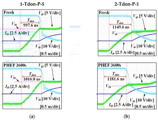
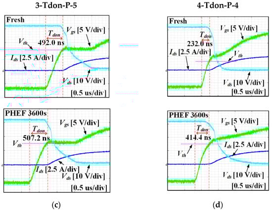
Figure 12.
Turn on waveforms in PHEF stress: (a) 1-Tdon-P-1, (b) 2-Tdon-P-2, (c) 3-Tdon-P-1, and (d) 4-Tdon-P-4.
Figure 13 shows all of the results of the Tdon experiment in PHEF stress according to the type of the switching device. Figure 13a–c indicate that there is no significant increase or decrease in Tdon according to PHEF stress for Si-based devices. However, in the case of SiC MOSFETs, an increasing trend of Tdon was observed in PHEF stress, similar to Vth in Figure 7d. At 900 s of PHEF stress, Tdon rose sharply and continued to increase. In particular, 4-Tdon-P-4 had a very large variation of about 80% in Tdon compared to the fresh condition after 3600 s of PHEF stress. Other SiC MOSFETs increased by 40% to 50% compared to the initial value. Based on Figure 12 and Figure 13, it can be seen that SiC MOSFETs have a more considerable Tdon increment during PHEF stress compared to Si-based devices.
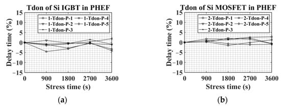
Figure 13.
Tdon variations in PHEF stress: (a) Si IGBT, (b) Si MOSFET, (c) Si IGBT with SiC diode, and (d) SiC MOSFET.
Figure 14represents some of the results of the Tdon experiment in NHEF stress. Figure 14 shows that no significant change in Tdon was observed for Si-based devices under NHEF stress. However, the Tdon of 4-Tdon-N-2 was reduced after NHEF stress. Tdon of 4-Tdon-N-2 in the fresh condition was 293.6 ns. Moreover, 4-Tdon-N-2 after NHEF stress was 248 ns. Therefore, the Tdon variation of 4-Tdon-N-2 was −16%. This change is opposite to the trend in the PHEF stress of SiC MOSFET. Tdon of 4-Tdon-N-2, a SiC MOSFET, was reduced because Vth decreased after NHEF stress.
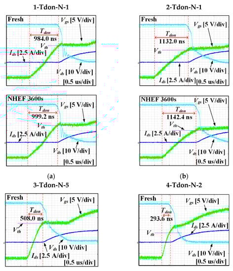
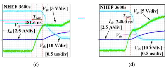
Figure 14.
Turn on waveforms in NHEF stress: (a) 1-Tdon-P-1, (b) 2-Tdon-P-2, (c) 3-Tdon-P-1, and (d) 4-Tdon-P-4.
Figure 15 shows all the results of the Tdon experiment in NHEF stress. Figure 15a–c describe that there was no significant change in Tdon of Si IGBT, Si MOSFET, and Si IGBT with SiC diode under NHEF stress. However, in SiC MOSET, Figure 15d shows that Tdon decreased as the NHEF stress progressed. After 3600 s of NHEF stress, the average Tdon of the five SiC MOSFETs decreased by about 13% compared to the initial value. The Tdon of SiC MOSFET decreases with the NHEF stress due to the reduction of Vth. As shown in Figure 2, Tdon is reduced as Vth decreases. Figure 8d shows that Vth of SiC MOSFET decreased after NHEF stress. Therefore, the Tdon of SiC MOSFET is reduced under NHEF stress.
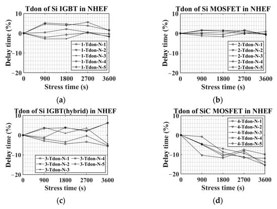
Figure 15.
Tdon variations in NHEF stress: (a) Si IGBT, (b) Si MOSFET, (c) Si IGBT with SiC diode, and (d) SiC MOSFET.
5.2. Turn-Off Delay Variation under HEF Stress
Figure 16 shows some of the results of the Tdoff experiment in PHEF stress. As shown in Figure 16, in the case of 1-Tdoff-P-1, 2-Tdoff-P-2, and 3-Tdoff-P-1, the difference between before and after PHEF stress was not clear. However, Tdoff of 4-Tdoff-P-4, as shown in Figure 16d, decreased sharply after PHEF stress. The Tdoff variation of 4-Tdoff-P-4 was −42%. This reduction in Tdoff can be explained by a change in Vm. Looking at the change in Vm before and after PHEF stress shown in Figure 16d, it can be seen that Vm increased after PHEF stress. Therefore, the Tdoff of the SiC MOSFET, 4-Tdoff-P-4, is reduced.
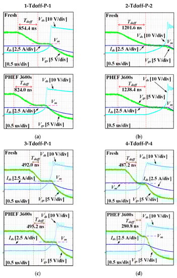
Figure 16.
Turn off waveforms in PHEF stress: (a) 1-Tdoff-P-1, (b) 2-Tdoff-P-2, (c) 3-Tdoff-P-1, and (d) 4-Tdoff-P-4.
Figure 17 is all the results of the Tdoff experiment in PHEF stress. For Si IGBT, Si MOSFET, and Si IGBT with SiC diode, Figure 17a–c demonstrate that there was no clear trend of increase or decrease in Tdoff in PHEF stress. However, in the case of SiC MOSFETs, Tdoff decreased steadily and sharply under PHEF stress. The average Tdoff variation of SiC MOSFET after 3600 s of PHEF stress was −46%. In PHEF stress, as shown in Figure 7d, Vth increases. In addition, Equation (7) indicates that when Vth increases, Vm also increases. The rise of Vm decreases Tdoff, as illustrated in Figure 3. Therefore, under PHEF stress, the Tdoff of SiC MOSFET is reduced, as shown in Figure 17d. Consequently, the Tdoff of SiC MOSFET is significantly reduced under PHEF stress compared to other Si-based devices. Figure 18 is some of the results of the Tdoff experiment in NHEF stress. Figure 18a–c indicate that Si-based devices did not have much change in Tdoff in NHEF stress. However, Tdoff of 4-Tdoff-P-4 had a noticeable difference. Tdoff of 4-Tdoff-P-4 in the fresh condition was 452.0 ns. Moreover, the Tdoff of 4-Tdoff-P-4 after 3600 s of PHEF stress was 560.8 ns. Therefore, the Tdoff variation of 4-Tdoff-P-4 was 24%. Figure 18d demonstrates that Vm decreased after NHEF stress. As shown in Figure 3, decreasing Vm raises Tdoff. Therefore, the Tdoff of 4-Tdoff-P-4 increased.
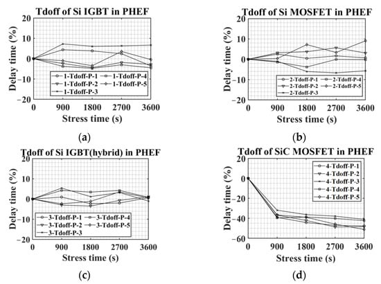
Figure 17.
Tdoff variations in PHEF stress: (a) Si IGBT, (b) Si MOSFET, (c) Si IGBT with SiC diode, and (d) SiC MOSFET.
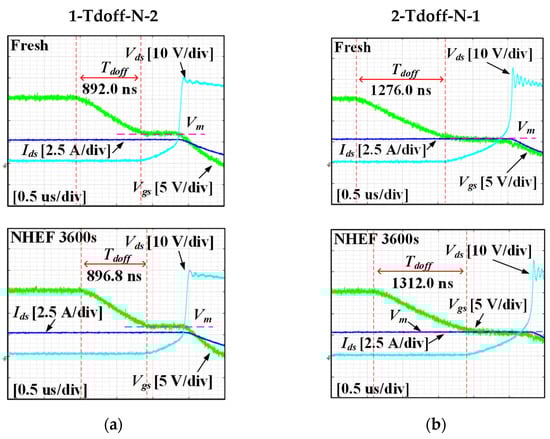
Figure 18.
Turn off waveforms in NHEF stress: (a) 1-Tdoff-P-1, (b) 2-Tdoff-P-2, (c) 3-Tdoff-P-1, and (d) 4-Tdoff-P-4.
Figure 19 represents all the results of the Tdoff experiment in NHEF stress. For Si-based devices, no clear trend was observed in NHEF stress. However, as shown in Figure 19d, the Tdoff of SiC MOSFETs increased as the NHEF stress continued. The average Tdoff of SiC MOSFETs after 3600 s of PHEF stress was 24%. In particular, 4-Tdoff-N-3 showed a significant change as Tdoff increased by about 33% compared to the initial value. It was mentioned in the previous discussion that the decrement of Vth raises Tdoff. Figure 8d demonstrates that Vth decreases with NHEF stress. Therefore, Tdoff rises in NHEF stress. Table 3 summarizes changes in Vth, Ron, Tdon, and Tdoff under HEF stress according to switch types. The values in Table 3 are results obtained after 3600 s of HEF stress. Table 3 demonstrates that Vth, Ron, Tdon, and Tdoff variations of SiC MOSFET are larger than those of Si-based devices.
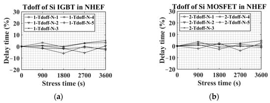
Figure 19.
Tdoff variations in NHEF stress: (a) Si IGBT, (b) Si MOSFET, (c) Si IGBT with SiC diode, and (d) SiC MOSFET.
Table 3.
Threshold voltage, on-resistance, turn-on delay, and turn-off delay variations according to switch types under HEF stress.
6. Performance of Voltage and Current Source Inverter with Duty Error Changes
The previous experimental results demonstrate that Tdon and Tdoff change after HEF stress. In other words, it means that the duty error of the converter changes as the gate oxide degradation progresses. This section analyzes the effects of duty error change according to HEF stress on the performance of voltage source and current source inverter. In the characteristic analysis according to HEF stress, a large gate resistance was used to sensitively observe changes in Tdon and Tdoff. Tdon and Tdoff of SiC MOSFET using a practical gate resistance of 15 Ω are shown in Figure 20.
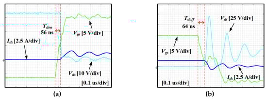
Figure 20.
Turn-on and turn-off waveforms when Rg = 15 Ω: (a) turn-on, and (b) turn-off.
Figure 20 shows the turn-on and turn-off waveforms when Rg is 15 Ω. As shown in Figure 20, a smaller Rg results in shorter Tdon and Tdoff because Vgs changes faster. However, since Vth, which is a parameter that determines Tdon and Tdoff, is the same regardless of Rg, the ratio of the change in Tdon and Tdoff according to Vth variation is similar even if Rg is different. Therefore, the rate of change of Tdon and Tdoff according to the HEF stress time obtained in this paper is applicable even when Rg is 15 Ω. As shown in Figure 20, when Rg is 15 Ω, Tdon is 56 ns, and Tdoff is 64 ns. In order to calculate the change of duty error according to the HEF stress time, it is necessary to know the rate of change of Tdon and Tdoff according to the stress time. As shown in Figure 13d, Figure 15d, Figure 17d and Figure 19d, Tdon, and Tdoff in each condition were obtained using five devices. Using the average value of the five devices, the rate of change of Tdon and Tdoff in PHEF and NHEF stress can be calculated. Figure 21 shows the rate of change of Tdon and Tdoff obtained by average values of results in Figure 13d, Figure 15d, Figure 17d and Figure 19d. In Figure 21, Ratedon represents the change rate of Tdon according to stress time, and Ratedoff means the change rate of Tdoff according to stress time.
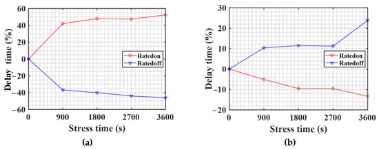
Figure 21.
Ratedon and Ratedoff according to the stress time in PHEF and NHEF stress: (a) PHEF stress, and (b) NHEF stress.
6.1. Performance Variation of Grid-Connected Voltage Source Inverter with Duty Error Change Due to Gate Oxide Degradation
This section examines the performance variation of the grid-connected voltage source inverter according to the duty error change due to the gate oxide degradation. Figure 22 shows a typical grid-connected voltage source inverter.

Figure 22.
Grid-connected voltage source inverter.
In general, a grid-connected voltage source inverter is controlled with a current alone or a current and power simultaneously [23]. Figure 22 shows a grid-connected voltage source inverter with both current and power controls. In Figure 22, Sv1, Sv2, Sv3, Sv4, Sv5, and Sv6 mean the switches of the voltage source inverter. In addition, Vdc is the inverter input voltage, and Cdc is the inverter input capacitor. Rl and Ll are line resistance and line inductance, respectively. Moreover, Lf and Cf mean the inductance and capacitance of the LC filter of the inverter output, respectively. Vg indicates the grid voltage, and ig represents the grid current. The voltage source inverter in Figure 22 simultaneously controls the grid current and instantaneous power. For the inverter control, first, the three-phase grid voltage and grid current are converted using abc to αβ transformation. The abc to αβ transformation is as (12). In (12), iga, igb, and igb are a-phase, b-phase, and c-phase grid current, respectively. Moreover, vga, vgb, and vgb are a-phase, b-phase, and c-phase grid voltages, respectively:
Using the α and β values of the three-phase grid voltage and current converted by (12), the instantaneous active power (P) and reactive power (Q) are calculated as in (13):
The instantaneous reactive power must be controlled to zero for the unity power factor control. Therefore, the reference of the instantaneous reactive power, denoted by Q*, is set to zero. Moreover, the reference of the instantaneous active power is applied as a desired value. In Figure 22, P* means the reference of the instantaneous active power. The instantaneous power calculated by (13) and its reference value are inputs to the PI controller for the power control.
Figure 23 shows the PI controller for the power control. The PI controller for the active power control generates an output value by amplifying and integrating the difference between P* and P, as shown in Figure 23. The output value of the active power becomes . Similarly, for the reactive power control, the output value, , is generated by amplifying and integrating the difference between Q* and Q. and mean the reference value of the d and q value of the grid current. Kpp, Kip, Kpq, and Kiq in Figure 23 represent coefficients used in the PI controller for the power control.
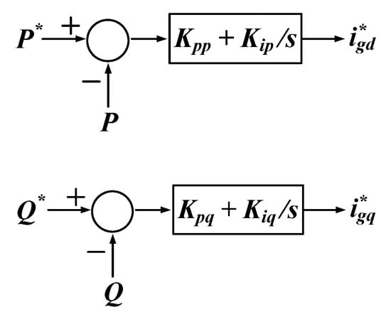
Figure 23.
PI controller for power control.
Meanwhile, for the grid current control, the d and q values of the grid current are required. By (14), the d and q values of the grid current are obtained:
In (14), θ is the phase of the grid voltage and is calculated through a phase-locked loop (PLL). The grid current reference values, which are the output of the PI controller for the power control, and the d and q values of the grid current from (14) are applied as the inputs of the PI controller for the grid current control.
Figure 24 shows the PI controller for the grid current control. As shown in Figure 24, to control the d value of the grid current, the output of the PI controller is generated by amplifying and integrating the difference between the reference value and the actual value of igd. The output of the PI controller controlling igd is , which is the d value of the voltage source inverter control signal. Similarly, to control the q value of the grid current, the output is generated by amplifying and integrating the difference between the reference value and the actual value of igq. means the q value of the voltage source inverter control signal. The reference values of igd and igq, which are expressed as and are the output of the PI controller for the power control, shown in Figure 23. Kpgd, Kigd, Kpgq, and Kigq in Figure 24 mean coefficients used in the PI controller for the grid current control.
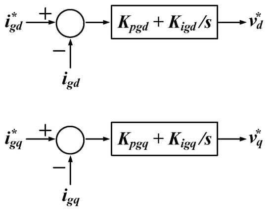
Figure 24.
PI controller for grid current control.
and undergoes dq to αβ conversion and αβ to abc conversion, resulting in , , and .The switching signals of the voltage source inverter are generated using space vector modulation [24]. The space vector modulation is implemented using an offset voltage, as shown in Figure 25 [25].
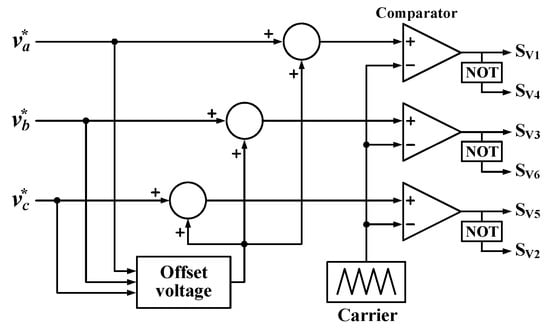
Figure 25.
Space vector modulation using the offset voltage.
Figure 25 shows the space vector modulation using the offset voltage. , , and in Figure 25 are the inverter control signal of a-phase, b-phase, and c-phase, respectively., , and are obtained from dq to αβ conversion and αβ to abc conversion of and . The offset voltage is calculated as follows (15):
In (15), voff means the offset voltage for the space vector modulation. Moreover, the largest of , , and becomes Vmax and the smallest becomes Vmin. Switching signals are generated by comparing the carrier with the values obtained by adding the offset voltage to , , and . Note that the switching frequency of the inverter is determined by the frequency of the carrier. In the voltage source inverter, the switches of one leg operate complementarily. Since a huge current can flow at the moment when all the switches of one leg of the voltage source inverter are on, the dead-time is set to make all switches of one leg be off when the switching state changes. In addition, the duty of the switch is changed by Tdon and Tdoff. Figure 26 shows gating signals and the a-phase pole voltage considering the dead time, Tdon, and Tdoff of Sv1 and Sv4 which are the a-phase switches of the grid-connected voltage source inverter in Figure 22.
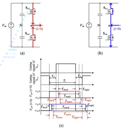
Figure 26.
Current path and gating signals of Sv1 and Sv4 considering dead time, Tdon, and Tdoff. (a) current path in i > 0 (b) current path in i < 0 (c) gating signals of Sv1 and Sv4.
In Figure 26, Td means the dead time. Furthermore, VaN is the a-phase pole voltage. Tr is the ideal dwelling time of VaN. Tactp/f is the dwelling time of VaN considering Td, Tdon, and Tdoff when the switching devices are fresh and the pole current (i) is positive. In addition, Tactn/f is the dwelling time of VaN considering Td, Tdon, and Tdoff when the switching devices are fresh and the pole current is negative. Tdon/a and Tdoff/a denote turn-on delay and turn-off delay in aged condition, respectively. Moreover, Tactp/a is the dwelling time of VaN considering Td, Tdon, and Tdoff when the switching devices are aging and the pole current is positive. In addition, Tactn/a is the dwelling time of VaN considering Td, Tdon, and Tdoff when the switching devices are aging, and the pole current is negative. Figure 26a,b show the current path according to the pole current direction. Figure 26a,b demonstrate that the dwell time of VaN changes, as shown in Figure 26c, because the path through which the current flows varies according to the sign of the pole current [26]. Equation (16) represents Tactp/f and Tactn/f:
Equation (16) becomes as (17) when aging is considered:
Tdon/a and Tdoff/a in (17) can be calculated through (18):
In (18), Ratedon and Ratedoff can be obtained from Figure 21. Meanwhile, the duty error due to aging can be calculated as (19) using (17) and the voltage source inverter switching frequency (Fswv):
In (19), Depv means the duty error of the voltage source inverter due to the gate oxide degradation when the pole current is positive. Denv also represents the duty error of the voltage source inverter due to the gate oxide degradation when the pole current is negative. Figure 27 shows the duty error of the voltage source inverter according to the aging stress time.
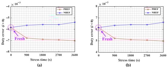
Figure 27.
Duty error according to stress time (a) i > 0, and (b) i < 0.
Figure 27a shows the duty error according to the stress time when the pole current is positive. When the pole current is positive, the duty error increases at PHEF stress and decreases at NHEF stress. Figure 27b shows the duty error according to the stress time when the pole current is negative. When the pole current is negative, the duty error at PHEF stress decreases and the duty error at NHEF stress increases. In this chapter, the effects of the change in the duty error due to the gate oxide degradation on the output of the grid-connected inverter are analyzed through simulation. The parameters of the inverter used in the simulation are summarized in Table 4.
Table 4.
Parameters of grid-connected voltage source inverter.
Figure 28 shows the simulation results of the grid-connected voltage source inverter according to HEF stress. Figure 28a–c are simulation results when using the duty error calculated from the fresh condition, PHEF stress during 3600 s, and NHEF stress during 3600 s, respectively. Figure 28 demonstrates that the THD of the grid current is the highest when the NHEF stress is applied for 3600 s. In addition, the peak-to-peak value of P is the largest in the case of PHEF stress. Moreover, the peak-to-peak value of Q is the largest in the case of NHEF stress.
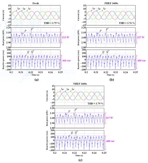
Figure 28.
Simulation results of the grid-connected voltage source inverter according to HEF stress: (a) fresh condition, (b) PHEF stress during 3600 s, and (c) NHEF stress during 3600 s.
Figure 29 showsgraphs summarizing the THD of the grid current and the peak-to-peak values of the instantaneous power according to the stress time. Figure 29 indicates that as the gate oxide degradation progresses, the quality of the grid current and the reference tracking ability of the voltage source inverter deteriorates.
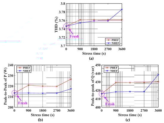
Figure 29.
Performance change of voltage source inverter under HEF stress time: (a) THD, (b) peak-to-peak value of P, and(c) peak-to-peak value of Q.
Figure 30 shows experiment waveforms of a three-phase voltage source inverter with RL load. A-phase of the inverter in Figure 30 was composed of SiC MOSFETs aged with PHEF stress. In addition, the remaining phases were composed of fresh SiC MOSFETs. Figure 30a represents the waveforms when the upper switch of a-phase is turned on. In Figure 30a, Vds_Sau means the Vds of the upper switch of a-phase. Furthermore, Vgs_Sau represents the Vgs of the upper switch of a-phase. Moreover, Ids_Sau is the Ids of the upper switch of a-phase. Figure 30a shows that the turn-on delay of the a-phase upper switch is 60 ns. Figure 30b is the three-phase current waveform of the inverter. In Figure 30b, iLa, iLb, and iLc represent the a-phase, b-phase, and c-phase inverter currents, respectively. Figure 30b demonstrates that the shape of the waveform hardly changes even when a-phase is aged.Therefore, Figure 30b shows that the aging degree of the inverter cannot be monitored by the load current shape.
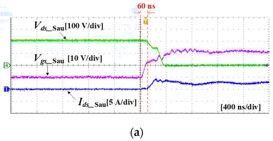
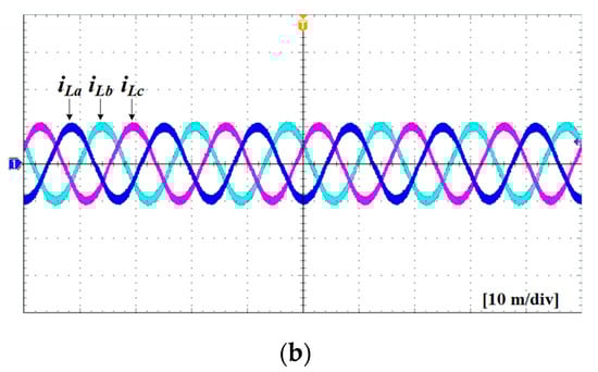
Figure 30.
Experiment waveforms of three-phase voltage source inverter with RL load: (a) turn-on waveform of aged a-phase upper switch, and (b) three-phase load current with aged a-phase.
6.2. Performance Variation of Current Source Inverter with Duty Error Change Due to Gate Oxide Degradation
This section examines the performance variation of the current source inverter (CSI) according to the duty error change due to the gate oxide degradation. Figure 31 shows a three-phase CSI.
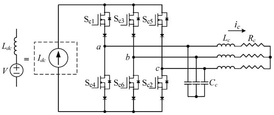
Figure 31.
Three-phase CSI.
In Figure 31, Sc1, Sc2, Sc3, Sc4, Sc5, and Sc6 represent the switches of the CSI. Additionally, Rc and Lc are the load resistor and inductor, respectively. Moreover, ic means the output current of the current source inverter. Idc is the input DC current supplied by the current source which can be expressed as a voltage source (V) and an inductor (Ldc) connected in series. Ldc represents the DC link inductor. Cc is the output capacitor required to drive the current source inverter. The current source inverter is usually controlled by space vector modulation [27].
In the CSI, Idc on the input side must flow without interruption. If the path through which Idc can flow disappears, an overvoltage is induced in Ldc. The voltage induced by the variation of Idc is expressed by (20). In (20), VLdc denotes a voltage induced in Ldc. Therefore, in the current source inverter, the overvoltage in Ldc is prevented by setting the overlap time when the switching state changes:
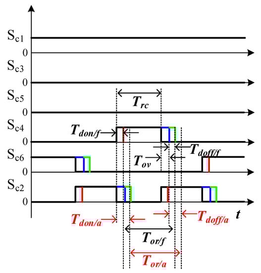
Figure 32.
Gating signals of CSI.
In Figure 32, Tov means the overlap-time set in advance when outputting the switching signals. In addition, Tor/f means the dwelling time of the switching signal considering Tov, Tdon, and Tdoff in the fresh state. Moreover, Tor/a represents the dwelling time of the switching signal considering Tov, Tdon, and Tdoff in the aged state. Trc indicates the dwelling time of the switching signal under ideal conditions. Tor/f and Tor/a are calculated through (21):
Tdon/a and Tdoff/a in (21) are calculated by (18). From (21), the duty error of the CSI when it is aged can be obtained as (22):
In (22), Dec means the duty error of the CSI according to aging. Moreover, Fswc represents the switching frequency of the CSI. Figure 33 shows the duty error of the CSI according to the HEF stress time. As shown in Figure 33, the duty error decreases under PHEF stress and increases under NHEF stress.
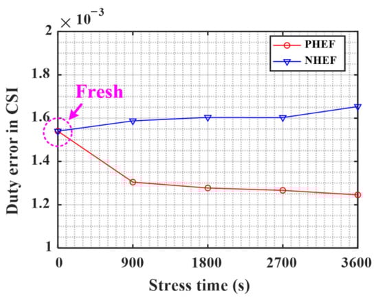
Figure 33.
Duty error in CSI according to HEF stress time.
A simulation was conducted to find out the effect of the change in duty error due to the gate oxide degradation on the CSI output current THD. Using the simulation, the THD of the output current of the CSI according to the duty error is examined. The CSI is controlled through space vector modulation, and open-loop control is performed. The parameters of the CSI used in the simulation are shown in Table 5.
Table 5.
Parameters of CSI.
Figure 34 shows the simulation results of the CSI according to HEF stress. ica, icb, and icc in Figure 34 represent the a, b, and c-phase output currents of the CSI, respectively. Figure 34 demonstrates that simulation results at PHEF stress have the smallest THD of the output current. In addition, the output current quality at NHEF stress is the worst.
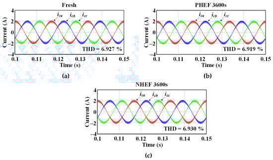
Figure 34.
Simulation results of the CSI according to HEF stress: (a) fresh condition, (b) PHEF stress during 3600 s, and (c) NHEF stress during 3600 s.
Figure 35 summarizes the average of the three-phase output current of the CSI according to the stress time. Figure 35 shows that in the case of PHEF stress, where the duty error decreases with the stress time, the THD of the three-phase output current is reduced as the stress time increases. However, in the case of NHEF stress, the THD of the output current slightly increases because the duty error rises with the stress time.
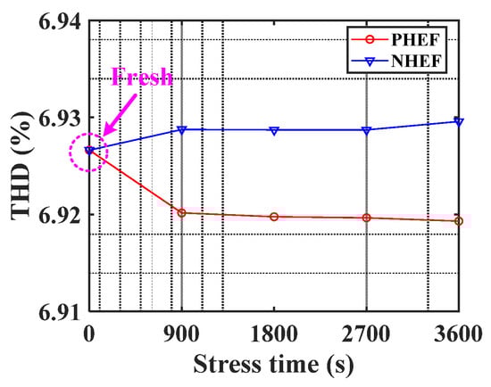
Figure 35.
THD of the output current of the CSI according to HEF stress.
7. Conclusions
This paper conducted studies on the changes in Tdon and Tdoff of SiC MOSFETs due to the gate oxide degradation. In addition, the performance variations of voltage and current source inverters due to changes in Tdon and Tdoff were examined. As a result, it was confirmed that Tdon and Tdoff of SiC MOSFETs significantly changed compared to other Si-based devices under the gate oxide degradation. In addition, variations in Tdon and Tdoff due to the gate oxide degradation worsened the output performance of the voltage source inverter. Moreover, changes in Tdon and Tdoff due to the negative gate oxide degradation reducing Vth declined the output performance of the current source inverter. These results indicate that the output performances of the SiC MOSFET-based voltage and current source inverter deteriorate under gate oxide degradation.
Author Contributions
Conceptualization, S.K. and S.C.; methodology, S.K. and S.C.; software, J.K.; validation, J.K.; formal analysis, J.K.; investigation, J.K.; resources, S.K.; data curation, J.K.; writing—original draft preparation, J.K.; writing—review and editing, S.K. and S.C.; visualization, J.K.; supervision, S.K.; project administration, S.K.; funding acquisition, S.K. All authors have read and agreed to the published version of the manuscript.
Funding
This work was supported by Technology Development Program to Solve Climate Changes through the National Research Foundation of Korea(NRF) funded by the Ministry of Science, ICT (2021M1A2A2060313) and the Korea Electric Power Corporation (Grant number: R21XA01-3).
Conflicts of Interest
The authors declare no conflict of interest.
References
- Zhang, C.; Liu, S.; Li, S.; Ma, Y.; Lu, W.; Huang, J.; Sun, W.; Yang, Z.; Zhu, Y.; Ni, L. Investigation on the Degradation Mechanism for GaN Cascode Device Under Repetitive Hard-Switching Stress. IEEE Trans. Power Electron. 2021, 37, 6009–6017. [Google Scholar] [CrossRef]
- Hazra, S.; Madhusoodhanan, S.; Moghaddam, G.K.; Hatua, K.; Bhattacharya, S. Design considerations and performance evaluation of 1200-V 100-A SiC MOSFET-based two-level voltage source converter. IEEE Trans. Ind. Appl. 2016, 52, 4257–4268. [Google Scholar] [CrossRef]
- Jahns, T.M.; Sarlioglu, B. The incredible shrinking motor drive: Accelerating the transition to integrated motor drives. IEEE Power Electron. Mag. 2020, 7, 18–27. [Google Scholar] [CrossRef]
- Pu, S.; Yang, F.; Vankatalapati, B.T.; Akin, B. Aging mechanisms and accelerated lifetime tests for SiC MOSFETs: An overview. IEEE J. Emerg. Sel. Top. Power Electron. 2022, 10, 1232–1254. [Google Scholar] [CrossRef]
- Ugur, E.; Xu, C.; Yang, F.; Pu, S.; Akin, B. A new complete condition monitoring method for SiC power MOSFETs. IEEE Trans. Ind. Electron. 2021, 68, 1654–1664. [Google Scholar] [CrossRef]
- Luo, H.; Iannuzzo, F.; Baker, N.; Blaabjerg, F.; Li, W.; He, X. Study of current density influence on bond wire degradation rate in SiC MOSFET modules. IEEE J. Emerg. Sel. Topics Power Electron. 2020, 8, 1622–1632. [Google Scholar] [CrossRef]
- Baba, S.; Gieraltowski, A.; Jasinski, M.; Blaabjerg, F.; Bahman, A.S.; Zelechowski, M. Active power cycling test bench for SiC power MOSFETs—Principles, design, and implementation. IEEE Trans. Power Electron. 2021, 36, 2661–2675. [Google Scholar] [CrossRef]
- Farhadi, M.; Yang, F.; Pu, S.; Vankayalapati, B.T.; Akin, B. Temperature-independent gate-oxide degradation monitoring of SiC MOSFETs based on junction capacitances. IEEE Trans. Power Electron. 2021, 36, 8308–8324. [Google Scholar] [CrossRef]
- Lelis, A.J.; Habersat, D.; Green, R.; Ogunniyi, A.; Gurfinkel, M.; Suehle, J.; Goldsman, N. Time Dependence of Bias-Stress-Induced SiC MOSFET Threshold-Voltage Instability Measurements. IEEE Trans. Electron. Devices 2008, 55, 1835–1840. [Google Scholar] [CrossRef]
- Xin, J.; Du, M.; Ouyang, Z.; Wei, K. Online monitoring for threshold voltage of SiC MOSFET considering the coupling impact on BTI and junction temperature. IEEE Trans. Electron. Devices 2021, 68, 1–6. [Google Scholar] [CrossRef]
- Aichinger, T.; Rescher, G.; Pobegen, G. Threshold voltage peculiarities and bias temperature instabilities of SiC MOSFETs. Microelectron. Rel. 2018, 80, 68–78. [Google Scholar] [CrossRef]
- Ye, X.; Chen, C.; Wang, Y.; Zhai, G.; Vachtsevanos, G.J. Online condition monitoring of power MOSFET gate oxide degradation based on miller platform voltage. IEEE Trans. Power Electron. 2017, 32, 4776–4784. [Google Scholar] [CrossRef]
- Jensen, W.R.; Foster, S.N. Online detection of MOSFET gate oxide degradation in a three-phase inverter-drive application. IEEE Trans. Transp. Electrif. 2021, 7, 50–57. [Google Scholar] [CrossRef]
- Yang, L.; Castellazzi, A. High temperature gate-bias and reverse-bias tests on SiC MOSFETs. Microelecton. Rel. 2013, 53, 1771–1773. [Google Scholar] [CrossRef]
- Gonzalez, J.O.; Wu, R.; Jahdi, S.; Alatise, O. Performance and reliability review of 650 V and 900 V silicon and SiC devices: MOSFETs, cascode JFETs and IGBTs. IEEE Trans. Ind. Electron. 2020, 67, 7375–7385. [Google Scholar] [CrossRef]
- Xie, M.; Sun, P.; Wang, K.; Luo, Q.; Du, X. Online Gate-Oxide Degradation Monitoring of Planar SiC MOSFETs Based on Gate Charge Time. IEEE Trans. Power Electron. 2022, 37, 7333–7343. [Google Scholar] [CrossRef]
- Karki, U.; Gonzalez-Santini, N.S.; Peng, F.Z. Effect of gate-oxide degradation on electrical parameters of silicon carbide MOSFETs. IEEE Trans. Electron. Devices 2020, 67, 2544–2552. [Google Scholar] [CrossRef]
- Zhang, L.; Yuan, X.; Zhang, J.; Wu, X.; Zhang, Y.; Wei, C. Modeling and implementation of optimal asymmetric variable dead-time setting for SiC MOSFET-based three-phase two-level inverters. IEEE Trans. Power Electron. 2019, 34, 11645–11660. [Google Scholar] [CrossRef]
- Liu, P.; Wang, Z.; Xu, Y.; Xiao, H.; Li, Y. Optimal overlap-time distribution of space vector modulation for current-source rectifier. IEEE Trans. Ind. Electron. 2021, 68, 4586–4597. [Google Scholar] [CrossRef]
- Karki, U.; Peng, F.Z. Effect of gate oxide degradation on electrical parameters of power MOSFETs. IEEE Trans. Power Electron. 2018, 33, 10764–10773. [Google Scholar] [CrossRef]
- Yang, F.; Pu, S.; Xu, C.; Akin, B. Turn-on delay based real-time junction temperature measurement for SiC MOSFETs with aging compensation. IEEE Trans. Power Electron. 2021, 36, 1280–1294. [Google Scholar] [CrossRef]
- Zhang, Z.; Dyer, J.; Wu, X.; Wang, F.; Costinett, D.; Tolbert, L.M.; Blalock, B.J. Online junction temperature monitoring using intelligent gate drive for SiC power devices. IEEE Trans. Power Electron. 2019, 34, 7922–7932. [Google Scholar] [CrossRef]
- Wen, B.; Boroyevich, D.; Burgos, R.; Mattavelli, P.; Shen, Z. Analysis of D-Q small-signal impedance of grid-tied inverters. IEEE Trans. Power Electron. 2016, 31, 675–687. [Google Scholar] [CrossRef]
- Wu, B.; Narimani, M. High-Power Converters and AC Drives; IEEE Press: Piscataway, NJ, USA, 2006. [Google Scholar]
- Blasko, V. Analysis of a hybrid PWM based on modified space-vector and triangle-comparison method. IEEE Trans. Ind. Appl. 1997, 33, 756–764. [Google Scholar] [CrossRef]
- Shen, Z.; Jiang, D. Dead-time effect compensation method based on current ripple prediction for voltage-source inverters. IEEE Trans. Power Electron. 2019, 34, 971–983. [Google Scholar] [CrossRef]
- Kim, J.; Kwak, S. Direct power control method with minimum reactive power reference for three-phase AC-to-DC matrix rectifiers using space vector modulation. IEEE Access 2019, 7, 67515–67525. [Google Scholar] [CrossRef]
Publisher’s Note: MDPI stays neutral with regard to jurisdictional claims in published maps and institutional affiliations. |
© 2022 by the authors. Licensee MDPI, Basel, Switzerland. This article is an open access article distributed under the terms and conditions of the Creative Commons Attribution (CC BY) license (https://creativecommons.org/licenses/by/4.0/).