Review

Charge Density Waves in Solids—From First Concepts to Modern Insights

Department of Physics, University of Zagreb Faculty of Science, Bijenička 32, 10000 Zagreb, Croatia
Symmetry 2025, 17(7), 1135; https://doi.org/10.3390/sym17071135
Submission received: 16 June 2025 / Revised: 4 July 2025 / Accepted: 10 July 2025 / Published: 15 July 2025
(This article belongs to the Section Physics)

Abstract

We present a brief overview of the field of charge density waves (CDW) in condensed systems with focus set to the underlying mechanisms behind the CDW ground state. Our intention in this short review is not to count all related facts from the vast volume of literature about this decades-old and still developing field, but rather to pinpoint the most important, mostly theoretical ones, presenting the development of the field. Starting from the “early days”, mainly based on weakly coupled, chain-like quasi-1D systems and Peierls instability, in which the Fermi surface nesting has been the predominant and practically paradigmatic mechanism of the CDW ground state stabilisation, we track the change in paradigms while entering the field of layered quasi-2D systems, with Fermi surface far away from the nesting regime, in which rather strong, essentially momentum-dependent interactions and particular reconstructions of the Fermi surface become essential. Examples of real quasi-1D materials, such as organic and inorganic conductors like Bechgaard salts or transition metal trichalcogenides and bronzes, in which experiment and theory have been extremely successful in providing detailed understanding, are contrasted to layered quasi-2D materials, such as high-T c superconducting cuprates, intercalated graphite compounds or transition metal dichalcogenides, for which the theory explaining an onset of the CDWs constitutes a frontier of this fast-evolving field, strongly boosted by development of modern ab initio calculation methods.

1. Introduction

The field of density waves (DW), namely charge density waves (CDW) and spin density waves (SDW), in condensed systems is a decades-old, still developing field with considerable impact on condensed matter physics, yielding a remarkable success in relating theory and experiment. As a rule of thumb, the appearance of DWs is related to so-called systems with “reduced dimensionality”, which in the real world refer to materials with highly anisotropic unit cells. In a simplified picture described in terms of three tight binding approximation (TBA) transfer integrals in three crystal directions, t x , t y and t z , we distinguish two particular principal classes: (1) t x t y t z , which we call “quasi-1D” systems, realised as crystal consisting of conducting chains weakly coupled in y-direction with coupling in z-direction practically negligible; (2) t x t y t z , which we call “quasi-2D” systems, realised as layered crystals with more or less weakly coupled isotropic planes. CDWs, among other ground states of broken symmetry, were observed in both classes. Instead of presenting all related physics from the vast volume of literature on the topic of CDWs (see, for example, collections [1,2,3,4,5]), or to repeat numerous reviews, our intention in this review is to pinpoint the most important facts related to the CDW ground state stabilisation, and depict the evolution of required theoretical paradigm between the “early days” quasi-1D and “nowadays” quasi-2D systems.
The first prediction of stabilisation of electron CDW ground state, through the instability of normal metal, was stated almost a hundred years ago by Sir Rudolf E. Peierls [6,7]. Essentially, the idea was that in a 1D metal with a half-filled electron band, if the every second atom in its crystal lattice is equally shifted (i.e., the lattice is dimerised), the gap would open due to the introduced periodic potential exactly at the Fermi level, leading to the lowering of electron band energy, thus stabilising the distorted configuration and turning a metal into insulator. If one perceives a 1D metal as a one-dimensional crystal with electron gas placed upon a chain-like crystal lattice where electrons are coupled to lattice vibrations (phonons), such a distortion may appear self-consistently. As it will be shown later, due to electron–phonon coupling, the phonon propagator undergoes a renormalisation of frequency proportional to the static susceptibility of an electronic system known as the Kohn anomaly [8,9]. As the latter quantity can attain large values—for example, the zero-temperature static susceptibility of 1D electron gas diverges at the wave vector Q = 2 k F connecting two points at ± k F ( k F is the Fermi wave number) constituting the Fermi surface in 1D—the phonon dispersion gets softened at that wave vector. That renormalisation can be large enough that at such a wave vector and certain temperature, the corresponding phonon mode attains a zero frequency, consequently “freezing” the lattice in the shape dictated by that particular phonon mode. Such a static lattice deformation appears through condensing a macroscopic occupation of the corresponding phonon displacement operator state, for which the energy is provided by the electronic subsystem, self-consistently forming the CDW. This mechanism of stabilisation is known as the Peierls-Fröhlich instability. The 1D electron band contribution to the condensation energy of such an ordered state features the characteristic logarithmic term in an ordered parameter contrasted to its square over the coupling strength, which in turn yields an exponential dependence of the zero-temperature order parameter on reciprocal coupling strength [10]. It implies that zero-temperature ordering can be established for arbitrarily small coupling. Electron–electron interactions, such as the Hubbard interaction that correlates electron spins for example, are generally in competition with electron–phonon coupling. In 1D systems with those prevailing, a similar type of instability based on divergent static susceptibility through the Stoner enhancement mechanism leads to an ordered antiferromagnetic ground state, comprising alternating electron spins along the undisturbed crystal lattice, known as the SDW ground state [11,12]. The further extension of this concept to spin–lattice interaction, involving elastic lattice coupled to electronic spin through the exchange interaction, leads to the so-called spin–Peierls transition, with spatially dimerised antiferromagnetic modulation, depending on parameters imposed by the system [13,14,15]. The subtle interplay of Coulomb interactions, electron spin, band filling and commensurability with the lattice may lead to different kinds of more complex orderings [16]. Although being a very important part of phase diagrams of many low-dimensional metallic systems at low temperatures, with a huge volume of literature covering the well-developed theory and related experiments, other ordered states apart from CDWs will not be covered in this short review, but only mentioned in places where their relation to CDWs appears to be important.
Since the real materials are always three-dimensional, one needs to determine those among them, as well as conditions under which, if any, the 1D physics briefly described above can be applied to. Among the aforementioned quasi-1D materials, there are metallic or semimetallic systems in which degrees of freedom along the third, z-direction can be neglected in a basic description, leaving layers of conducting ( x , y ) -planes with open Fermi surfaces due to high anisotropy of the unit cell. Such a class of materials is based on a weakly interconnected chain-like molecular structure, among them examples of organic conductors such as Bechgaard and Fabre salts, some transition-metal trichalcogenides, and bronzes [17,18,19,20,21]. In their description, the Fermi surface consists of two slightly corrugated sheets in a reciprocal space. If there exists a unique vector Q in the reciprocal space by which one can map one sheet exactly to another inside the Brillouin zone, we say that the Fermi surface possesses a property of the perfect nesting [22]. Vector Q is closely related to the 2 k F distance between the “left” and “right” sheet of the open Fermi surface. In that case, the electron band properties and related ground state induced by the static interaction at that particular wave vector can be one-to-one mapped onto the 1D Peierls mechanism, with a fully gapped Fermi surface and established DW ordering. Since in the real systems the Fermi surface nesting usually deviates from perfect, the interaction-driven electron scattering at wave vector Q usually creates pockets of particle states at the Fermi surface, leaving it only partially gapped, which in turn “cuts” the logarithmic singularity in the zero-temperature susceptibility. However, if these pockets are small enough, the zero-temperature susceptibility can still attain large enough values to trigger the Peierls-Fröhlich (Kohn anomaly) or Stoner mechanism and establish the CDW or SDW ground state with critical temperatures on the order between 1 K and 10 K [23]. The way to “restore” the perfect nesting, in a sense, is by applying a strong static magnetic field perpendicular to the sample plane. The Landau quantisation of 2D electron pockets at the Fermi surface transforms the electron spectrum to one-dimensional in quantum number, effectively restoring the perfect nesting since the states are degenerate at the Landau levels. As the magnetic field is increased, the position of the Fermi energy switches between adjacent Landau levels, consequently causing a cascade of phase transitions between DW ground states with abrupt change of the ordering wave vector related to the “active” Landau level. This phenomenon is called the field-induced density wave and is observable as the SDW cascade in systems with very small Fermi pockets of imperfect nesting and strong magnetic fields, since only a dozen such phases, counting from the zeroth Landau level (most pronounced) can be detected [24,25,26]. Furthermore, through the Pauli coupling of magnetic field to electron spin, SDW and CDW state gets hybridised and tuned by magnetic field [27,28,29,30], or may even be induced by magnetic breakdown through the delocalisation of Landau-quantised states and creation of magnetic bands [31,32]. The model based on the Fermi surface nesting and Peierls/Stoner instability, through the weak-coupling random phase approximation approach, has been working so well in terms of developed theory backed by experiments in wide class of quasi-1D materials, that it practically became a paradigm for the CDW and SDW physics over the last several decades.
However, the CDW ground state has been observed in an entirely different class of physical systems, the layered materials consisting of conducting planes with rather weak interaction between them. Among them, we single out examples of high-T c superconducting cuprates [33,34], intercalated graphite compounds (GIC) [35,36], and transition metal dichalcogenides (TMD) [37,38,39]. Their Fermi surfaces, while in the conducting ground state, are closed 2D contours. This class of materials is called quasi-2D and, regarding this topic, most of them share one important property: the Fermi surface is far away from nesting, yet the CDW appears as a possible ground state in the phase diagram, with critical temperature up to an order of 10 2 K. It seems that the nesting paradigm has been so deeply rooted in the onset of CDWs that a great part of the scientific community struggled for decades in various unsuccessful attempts to find some form of nesting, ceasing to pursue the real underlying mechanism. For some materials, this clutching at straws has even appeared to yield a partial success. For example, a very complex shape of the Fermi surface present in number of TMDs, involving the saddle band, permits the possibility of its close to nesting portions [40,41], or even nesting of higher order [42], but the critical temperatures predicted by the weak-coupling based susceptibility calculated within the standard random phase approximation (RPA) remained too high with respect to experiments. This approach, naturally, excludes most materials in which the Fermi surface possesses no nesting properties whatsoever, such as high-T c cuprates or intercalated graphite compounds. The nesting mechanism has, in fact, been challenged since the early 1980s by attempts to make the Kohn anomaly criterion more realistic by supplementing the standard weak-coupling model with lattice-related contributions such as electron Coulomb and exchange energies [43,44], and by taking into account anharmonic phonon self-energy contributions [45]. In the lack of nesting, the attempts to understand the CDW state have been primarily directed towards the role of strong, momentum-dependent electron–phonon interaction [46] which, together with phonon entropy taken into account (pinpointed quite some time ago in an early work by McMillan [47] although still related to some degree of nesting), appeared essential in understanding the softening of phonon modes related to the aforementioned Kohn anomaly and establishing the onset of CDW outside of the nesting paradigm [48]. Since then, among the novel concepts parting from the nesting requirement, several different directions have developed besides the previously mentioned one. For example, the onset of CDW can be related to a soft electronic mode, perceived as formation of an excitonic insulator, i.e., the condensate of electron–hole pairs periodic in space [49,50,51], or as a result of the strong coupling nature of the electronic structure in specific band configurations (through e.g., polarons) [52]. In this paper, we shall cover the approach mentioned first as it appears to be, so far, the most founded in the experiment. By that we do not exclude the other mechanisms as possible in certain materials. In considered systems, based on electron–phonon coupling and the Kohn anomaly, the zero-temperature CDW transition behaves as a quantum phase transition in the coupling strength domain. It appears yielding a finite order parameter only if the coupling strength has a value larger than the critical, determined by the properties of a material, particularly of the electron band. The essential contribution to the CDW condensation energy comes from an electron band that gets reconstructed in the process of self-consistent CDW formation, providing the energy for the condensation of a specific boson mode (i.e., phonon of specific wave vector through the Kohn anomaly) [53]. Apart from the rigorous mathematical model, it can be seen even intuitively whenever the wave number of the softened phonon mode typically attains the value involving the electronic 2 k F , related to the Fermi surface, instead of some other random value independent of the electronic subsystem. Such a band reconstruction in 2D predominantly leads to the significant reduction in the electron density of states (DOS) around the Fermi energy, forming so-called pseudo-gap, and creation of the logarithmic type of van Hove singularity below it [54]. The redistribution of electron states around the Fermi energy to lower energies in the van Hove singularity self-consistently leads to the stabilisation of the very ordering that created it, i.e., to the periodic CDW potential. The zero-temperature ground state can be grasped to the great extent even within the mean-field approximation, with the benefits of analytical approach revealing the very nature of the mechanism behind the CDW stabilisation, indicating condensation of the softest phonon mode, which manifests the strongest coupling to electrons exactly at the wave vector corresponding to the CDW in accordance with experiment, as demonstrated on an example of intercalated CaC 6 [35,55]. However, the material-specific quantitative description at finite temperatures requires a way more sophisticated ab initio approach, with special focus on phonon entropy and anharmonicity effects appearing to play the key role for the CDW stabilisation in that regime besides the essentially momentum-dependent strong electron–phonon coupling [56,57,58,59]. In a number of materials, it has been observed that the CDW ordering is augmented in the sense of increased magnitude of the order parameter and correlation length, in the presence of the strong magnetic field of several dozen Tesla perpendicular to the conducting plane of the sample [60,61,62]. Besides the basic Landau quantisation of closed Fermi pockets, such a strong magnetic field naturally involves the field-assisted over-gap tunnelling between them (magnetic breakdown) in systems with the CDW order parameter typically on the order of 10 2 K. In clean samples, with a typical electronic Larmor radius, small compared to its scattering length, this tunnelling of electron wave packages permits for coherent magnetic breakdown, creating the non-trivial interference effects and leading to the formation of magnetic bands. Such a subtle interplay of electron dynamics, involving the delocalisation of Landau quantised states, i.e., creating electron open orbits as well as restoring the closed ones, impacts the system in number of ways such as additionally stabilising the CDW state [63], inducing a field-driven change in the sign of the Hall coefficient [64,65]. Unconventional, huge quantum oscillations of otherwise non-oscillating classical magnetoconductivity appear alongside the standard Shubnikov-de Haas effect or is absent [66].
The main motivation and central goal of this review is to present the problem of the CDW formation from a specific angle, i.e., to grasp and compare the simplest theoretical frameworks that, for the sake of physical understanding, can be solved analytically, but still to contain basic mechanisms explaining the onset of the CDW ground state in Q1D and Q2D systems where the Fermi surface nesting, playing the key role in the first, does not appear to be the necessary requirement in the latter. Those, giving the qualitative and, up to the order of magnitude, quantitative understanding, can in no way substitute the advanced ab initio models that provide the material-specific quantitative results, but rather supplement them by providing a basic understanding of the background physical mechanisms of the investigated phenomenon. The paper is organised as follows: after this Introduction, there are three main sections. The first one covers the quasi-1D systems belonging to “the early days” of CDW physics, the second one covers some modern insights related to the quasi-2D systems, and finally we present the Conclusions. Each main section, covering quasi-1D and quasi-2D systems, is divided into subsections, first containing a brief description of relevant materials and experiments, then followed by the theoretical description of the main features related to the mechanism associated with the onset of the CDW ground state, as well as some of its most important properties.

2. Basic Model: Condensation Energy of the CDW State and Kohn Anomaly

The textbook definition of the condensation energy of the newly established ground state is the difference between the total ground state energy of that state and the total ground state energy of the initial state. If positive, it indicates the new stable ground state, implying that its total energy is lower than that of the initial state. We consider a system of interacting electrons and phonons on a 2D lattice as the basic model we adopt to understand the onset of the CDW state, and write the Hamiltonian as
H = H e l + H p h + H e l p h ,
where
H e l = k , σ ε ( k ) a k σ a k σ ,
H p h = q , η ω η ( q ) b q η b q η ,
H e l p h = 1 V k , q , σ , η g q η a k + q σ a k σ b q η + b q η
represent the one-electron band contribution, the phonon contribution and the contribution of electron–phonon coupling, respectively. We define the following quantities used in the above expressions: ε ( k ) is the initial one-electron band dispersion characterised by wave vector k = ( k x , k y ) , ω η ( q ) is the phonon dispersion characterised by wave vector q = ( q x , q y ) and polarisation vector η = ( η x , η y ) , g q η is the momentum- and polarisation-dependent electron–phonon coupling, V is the volume of the unit cell, σ electron spin (degenerate in our consideration), while a k σ and b q η are electron and phonon creation operators respectively. To describe the onset of the CDW state stabilised through the Kohn anomaly, it is obvious what kind of approximation on the electron–phonon coupling we apply: out of all dependencies we only keep the dependence on the phonon momentum and its polarisation; in general 2D systems, we need to distinguish possible coupling to different modes with different momenta. Such a CDW is established through the macroscopically large occupation of the phonon state with the wave vector Q and polarisation η , i.e., we have the non-vanishing expectation value of the corresponding phonon operator b Q η = b Q η 0 . Accordingly, within the mean-field approximation, which has many flaws but appears to be sufficient to grasp a basic analytical insight into the onset of the CDW state in both Q1D and Q2D systems, we define the CDW order parameter Δ exp ( i Φ ) 2 g Q η b Q η / V , where Δ and Φ are its amplitude and phase (in principle dependent on Q and η , but we omit explicitly writing it for the sake of simplicity). While phase Φ is not important in the model considering only the ground state, i.e., not considering processes involving some aspects of collective dynamics of the CDW, optimal values of Δ , Q and η are determined self-consistently by maximisation of condensation energy of the imposed CDW state with Δ 0 contrasted to the initial state with Δ = 0 . In that sense, the CDW is a periodic potential that, in principle, scatters electrons from the state k to states k ± n Q , where n is a positive integer. Among the Fourier harmonics of potential, we keep only n = 1 , which appears with the largest matrix element, consequently opening the largest gap in the electron spectrum, which would govern the CDW stabilisation process anyway. It implies that the self-consistent CDW potential is to be expected in the form of the simplest sinusoidal distribution of charge. The total mean-field Hamiltonian to be treated self-consistently reads [10]
H M F = k , σ ε ( k ) a k σ a k σ + Δ e i Φ a k + Q σ a k σ + Δ e i Φ a k Q σ a k σ + V ω Q η 2 g Q η 2 Δ 2 ,
where the first term represents the contribution of the electron band reconstructed by interaction, while the second term is often known as the “elastic” contribution coming from the crystal lattice that is statically deformed through the Kohn anomaly. The first term is straightforwardly diagonalised, yielding the (reconstructed) electron band dispersion
E ± ( k ) = 1 2 ε ( k Q 2 ) + ε ( k + Q 2 ) ± ε ( k Q 2 ) ε ( k + Q 2 ) 2 + 4 Δ 2 ,
where Δ appears as the gap parameter. The origin of reciprocal space is conveniently chosen at the point where the one-electron dispersions overlap and the Fermi surface reconstruction takes place by lifting the degeneracy, i.e., ε ( k ) , ε ( k + Q ) ε ( k Q / 2 ) , ε ( k + Q / 2 ) . Based on the second term, we define the dimensionless electron–phonon coupling constant
λ Q η g F 0 g Q η 2 ω Q η ,
where by g F 0 we denote an electron density of states in the metallic state, taken at the Fermi energy. Narrowing our basic consideration to zero temperature, the energy of the electron band is then
E b a n d ( Q , Δ ) = k , ν E ν ( k ; Q , Δ ) ,
where ν denotes all good quantum numbers such as spin, band, etc, while summation over wave vector goes up to the Fermi wave vector, the elastic energy of the deformed lattice is
E l a t t ( Q , Δ , η ) = g F 0 Δ 2 2 λ Q η ,
yielding the condensation energy of the CDW state
E CDW = E b a n d ( Δ = 0 ) E b a n d ( Δ 0 ) + E l a t t | Q , Δ , η = optimal ,
where E b a n d ( Δ = 0 ) = E b a n d ( Q , Δ = 0 ) and E b a n d ( Δ 0 ) = E b a n d ( Q , Δ 0 ) . Condensation energy E CDW , as a function, depends on parameters Q , Δ , η , whose values should be found self-consistently through the optimisation procedure to maximise it. As E l a t t is always positive, it is apparent that the gain in condensation energy that makes it positive, and by that stabilising the CDW state, should come from the band energy E b a n d ( Δ 0 ) which, through the reconstruction due to finite order parameter Δ , should appear to be lower enough with respect to the initial band energy E b a n d ( Δ = 0 ) .
The role of the electron subsystem also becomes evident through the Kohn anomaly, which is in essence the renormalisation of a phonon spectrum at a specific wave vector (suppression of frequency: “softening” of that particular mode) due to electron–phonon coupling. To obtain the expression for the renormalised energy of the phonon mode with the wave vector Q in the simplest way, yet sufficient to illustrate the physical background of the phenomenon, one can define equations of motion for phonon operators, describing the displacement of ions, coupled to electron density through a coupling constant g Q η , as described by the Hamiltonian (4) [10]. As the electronic dynamics is to the great extent adiabatic with respect to phonons (except in specific cases such as of considerably strong coupling, polaronic systems etc.), corresponding effective potential generated by the displacement of ions is related to electronic density through its zero-frequency density–density response function, i.e., static susceptibility χ ( Q , T ) , which measures the available phase space for that particular scattering process at temperature T. In essence, it directly determines the phonon self-energy due to coupling to electrons. The renormalised phonon frequency ω Q η r e n is then determined by the expression
ω Q η r e n 2 = ω Q η 2 + 2 ω Q η g Q η 2 χ ( Q , T ) ,
directly defining the instability condition, i.e.,
2 g Q η 2 ω Q η 1 χ ( Q , T ) ,
in which the critical temperature is determined by the point T = T c at which the left- and right-hand sides of expression (12) are equal. Electrons screen such potential, resulting in a negative response function χ . That, in turn, reduces the frequency of the corresponding phonon mode by virtue of Equation (11), depending on temperature T. This reduction may be severe enough to push the frequency ω Q η r e n to zero at temperature T c , effectively “freezing” the crystal lattice in the deformed shape, determined by phonon wave vector Q and polarisation η , and electron density modulated in the likewise way to provide optimal screening. In nature, this process appears spontaneously, where the system self-consistently picks Q and η (i.e., the phonon mode) for which the product of electron–phonon coupling and electron susceptibility is maximised at the highest temperature T c . This is a structural phase transition with critical temperature T c , in which the crystal lattice attains a new periodicity 2 π / Q and electron charge is redistributed in the form of CDW with wave vector Q along the polarisation direction η (see Figure 1). Particularly, in 1D systems, this is known as the Peierls–Fröhlich transition, where Q = 2 k F and CDW is governed entirely by the electron band properties.
The static electron susceptibility is given by the expression
χ ( q , T ) = 1 V k , σ f ε ( k ) f ε ( k + q ) ε ( k ) ε ( k + q ) ,
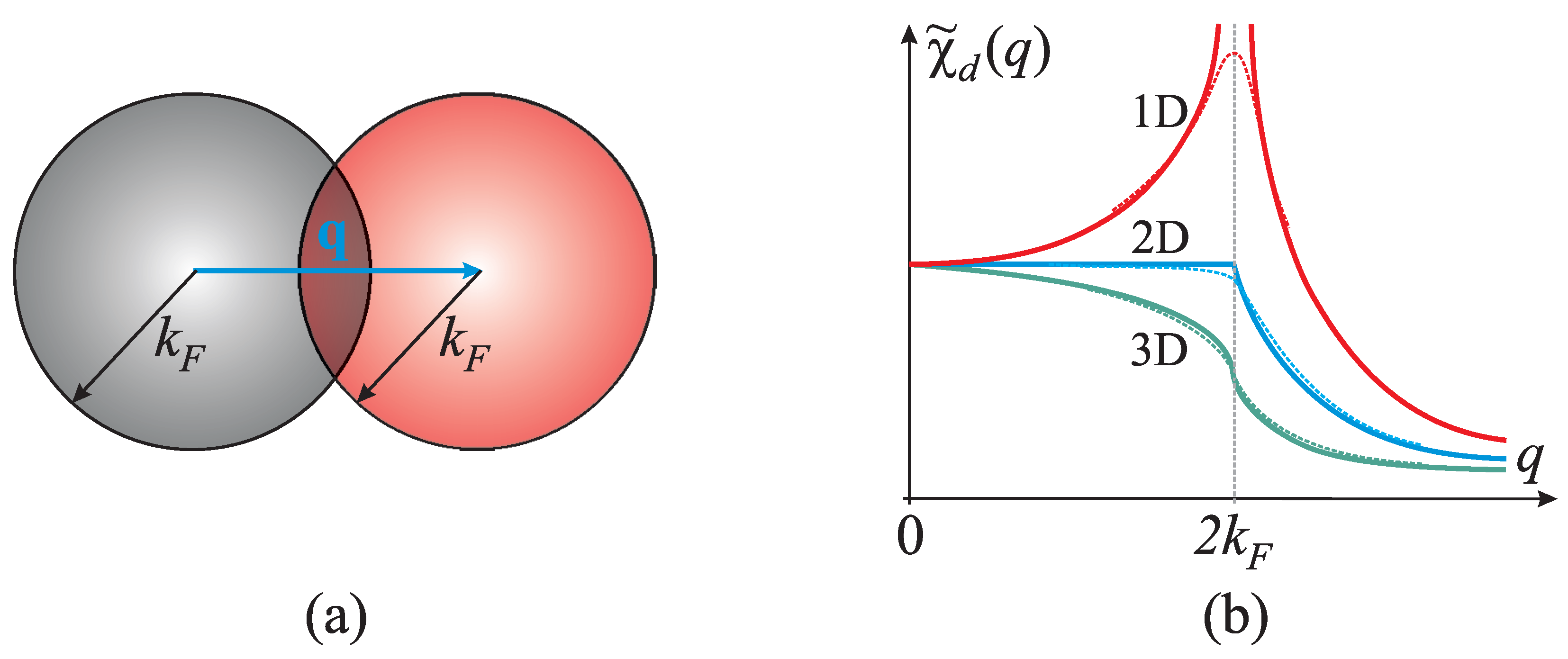
where f ( ε ) is the Fermi function at temperature T. For the simple metal with the band of the parabolic form ε ( k ) = 2 | k | 2 / 2 m , i.e., of the free electron gas with electron effective mass m, the zero-temperature result χ d ( q ) = g F ( d ) χ ˜ d ( q ) , with corresponding DOS is as follows:
g F 1 D = V 2 m π 2 k F , g F 2 D = V m π 2 , g F 3 D = V m k F π 2 2 ,
depending on the dimensionality of the system, d is
χ ˜ d ( q ) = k F q ln | 2 k F + q 2 k F q | , 1 D 1 Θ ( q 2 k F ) 1 2 k F q 2 , 2 D 1 2 + k F 2 q ln | 2 k F + q 2 k F q | , 3 D
as shown in Figure 2. We shall use and comment on this result in the sections that follow.

3. The Early Days: Quasi-1D Systems

3.1. Materials

Typically, the crystal structure of the quasi-1D class consists of molecular chains that are mutually interconnected in the sense of electron transfer. The unit cell is highly anisotropic in all three directions, consequently leading to huge differences between electron TBA transfer integrals t x t y t z , by an order of magnitude or more. Direction x along the chains is the highly conducting direction. Materials within that class are organic or inorganic room-temperature conductors, such as the following examples:
  • Bechgaard salts (TMTSF)2X, where TMTSF stands for tetramethyltetraselenafulvalene and X is an inorganic anion, e.g., PF 6 , AsF 6 , ClO 4 , ReO 4 , B, etc., or related Fabre salts (TMTTF)2X, where TMTTF stands for tetramethyltetrathiafulvalene, in which selenium is substituted with sulphur. The unit cell is of triclinic symmetry. The crystal structure consists of stacked TMTSF or TMTTF organic molecules with overlapping π -orbitals, resulting in high conductivity directed along the stacks, between which inorganic anions are placed. Those are so-called charge transfer salts in which 1/2 electrons are transferred from an organic molecule to an inorganic anion on average, resulting in three-quarter-filled electron bands. The slight structural dimerisation along the stacks, pronounced more in TMTTF than in TMTSF stacks, results in a small dimerisation gap opening and a half-filled conduction band. Typical low-temperature ground states, among others, are the spin–Peierls CDW, SDW, or superconductor, depending on the organic molecule and anion in the structure.
  • Transition metal trichalcogenides MX 3 , where M stands for group IV or V transition metal and X for chalcogen atom, such as NbSe 3 , TiSe 3 , TaS 3 , etc. The basic structural unit is a triangular prism MX 6 , with M in the centre, from which chains are formed by stacking them along a line. Depending on the material, there is a different number of neighbouring chains with slight geometrical variations (for example, in NbSe 3 , this number is three), resulting in triclinic ( NbSe 3 ) or monoclinic ( TaS 3 ) unit cell symmetry. The electron band is quarter-filled. The common low-temperature ground state of these materials is CDW.
  • Transition metal bronzes refer to the oxides of transition metals that may attain different crystal structures, i.e., layered or 3D structure of interconnected chains, with alkali metal atoms intercalated into the structure. The most well-known quasi-1D bronzes are those of molybdenum, X 0.3 MoO 3 , where X stands for K, Rb, or Tl, also known as “blue bronzes”. The structure is orthorhombic, with stacked MoO 6 clusters along the chain direction and alkali atoms intercalated between the chains. A rather complex band structure due to periodic distortion along the chains, resulting in a rather large unit cell, however, yields two overlapping, three-quarter-filled electron-conducting bands. This material is a typical low-temperature CDW system.
  • TTF-TCNQ (tetrathiafulvalene-tetracyanoquinodimethane) is an organic compound consisting of stacked planar molecules into parallel linear chains. Electrons are transferred from the TTF to TCNQ molecule (approximately 0.6 electrons per molecule), resulting in a partially filled electron band and room-temperature conducting properties. The low-temperature ground state is CDW.
  • α -(BEDT-TTF)4MHg(XCN)4, where BEDT-TTF = bis(ethylenedithio)tetrathiafulvalene, M = K, Tl and X = S, Se, is a monoclinic layered (conducting BEDT-TTF layers intertwined with insulating MHg(XCN)4 layers) organic charge-transfer salt with three-quarters-filled band. Together with open Fermi surface sheets, it also features closed Fermi pockets, with that involving its quasi-2D aspects. The low-temperature ground state is CDW.
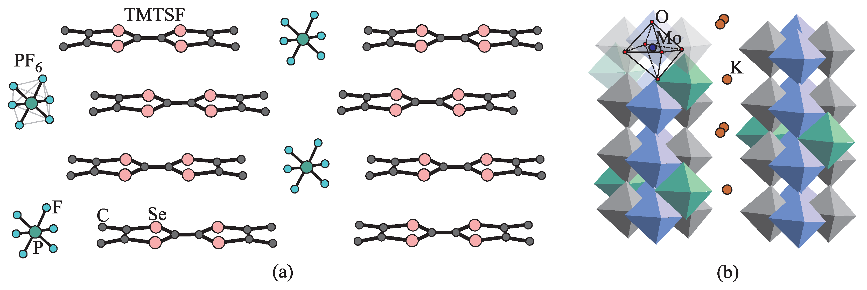
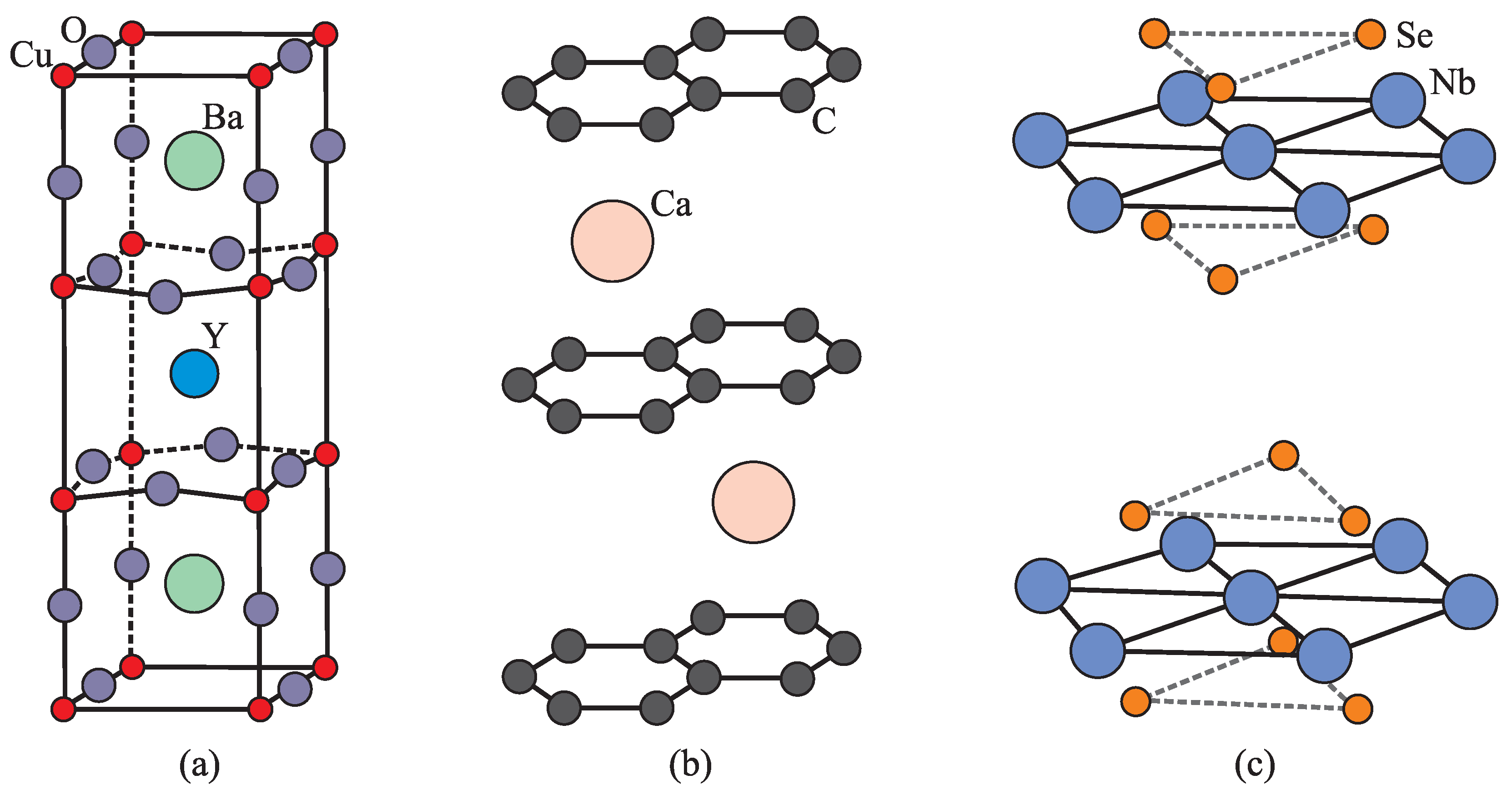
Schematic depiction of the crystal structure of two examples of quasi-1D materials is shown in Figure 3. The comprehensive overview of structural and electronic properties of quasi-1D materials can be found in the number of reviews, such as Refs. [17,18,19,20,21] and references within.
(TMTSF)2 PF 6 was the first, and probably the most studied organic conductor. The room temperature and ambient pressure lattice constants, a x 7.28 Å, a y 7.54 Å, a z 13.51 Å, comprise a triclinic unit cell of the volume of approximately 707.9 Å 3 . Under these conditions it has metallic properties, with Fermi energy of 6.1 eV and Fermi velocity on the order of 10 5 m/s, although with significantly lower concentration of carriers (∼ 10 3 Å 3 ) comparing to standard metals like copper (∼ 1 Å 3 ). The aforementioned weak structural dimerisation along the chains is important, among other things, because the band half-filling enhances the role of so-called umklapp processes of electron scattering, playing a decisive role in discrimination between CDW and SDW ground state stabilisation. The ground state of the system below 12 K at ambient pressure is the SDW, which under pressure higher than 6 kbar and below 1 K transitions into superconducting. On the other hand, the related (TMTTF)2 PF 6 salt is the ambient pressure spin–Peierls system below 19 K. Unlike the PF 6 anion, which is approximately centrosymmetric, the anions of tetrahedral shape, such as ClO 4 or ReO4 4 , can undergo an order–disorder transition into a spatially ordered state at low temperatures [67]. The additional periodic potential created by anion ordering may have nontrivial effects on the electron band, opening new gaps, and consequently altering properties of the ground state [68,69].
Due to reduced dimensionality of quasi-1D systems, implying the reduced phase space for electron scattering, interactions in such systems are modified and enhanced in a specific way [70]. A rather fascinating phenomenon appears in quasi-1D systems as one lowers the temperature from room temperature towards 1 K. At high temperature, the coherence is predominantly pronounced along the stacks (x-direction) due to strong thermal fluctuations, resulting in a one-dimensional motion in its character, manifesting the features of Luttinger liquid and related phenomena such as charge–spin separation, etc. As the temperature decreases, the scattering suppressing the inter-stack tunnelling is reduced, permitting the 2D motion in the ( x , y ) -plane first, and at even lower temperature for the full 3D motion, i.e., for the Fermi liquid. It is called the 1D → 3D dimensional crossover, which is important for the density wave or superconducting ground states that require 3D coherence to some degree to stabilise [71]. Furthermore, the low-temperature ground state of quasi-1D systems is very sensitive to hydrostatic pressure and magnetic field. As electronic TBA transfer integrals, determining the electron bands, which exponentially depend on the corresponding interatomic distance, the shape of the Fermi surface, and particularly its nesting properties, are essentially dependent on them, being tuned by an external pressure. The (small) deviations from the perfect nesting create electron pockets on the Fermi surface when they are scattered by interaction. In a strong, perpendicular magnetic field, those 2D pockets in the momentum plane undergo Landau quantisation, yielding the spectrum described by one quantum number, i.e., index of the Landau level, which effectively reduces dimensionality of the problem to 1D and in a sense restores the perfect nesting condition. As the magnetic field changes, depending on filling, the Landau level at which the nesting is best subsequently changes to the neighbouring one, causing the abrupt change of the corresponding wave vector. This results in the cascade of field-induced density wave phases (typically, but not exclusively of spin density waves, hence “FISDW”) in increasing magnetic field, described by nowadays practically paradigmatic standard model of quantised nesting [24,25].
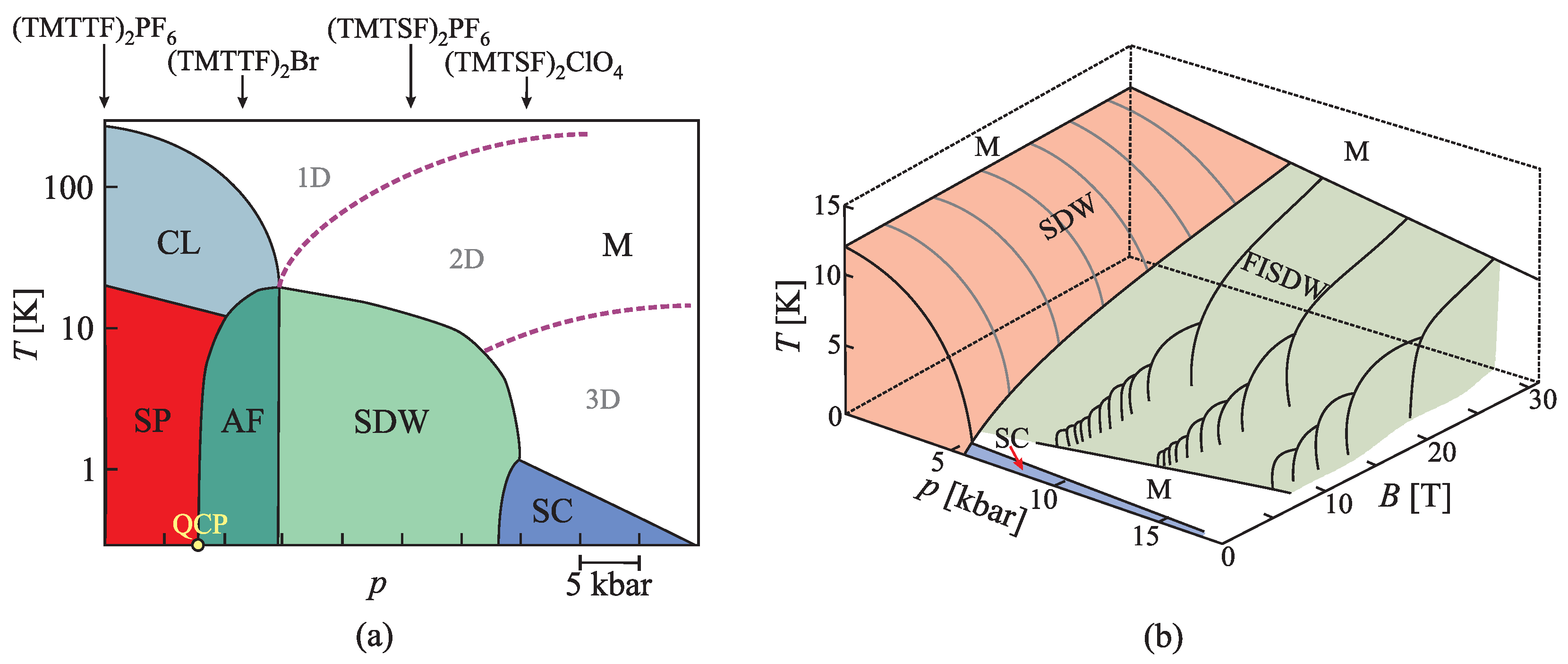
In summary, the quasi-1D materials have incredibly rich low-temperature phase diagrams, containing a variety of different phases governed by electrons “living” in the above-described environment, as shown by examples presented in Figure 4.

3.2. The Minimal Model of the CDW Transition in Quasi-1D Metal

In order to address the high anisotropy and open Fermi surface, we adopt the TBA description of a 2D metal, with the third dimension and deviation from the orthorhombic symmetry neglected in the first approximation. It is very important to stress that the description that follows is applicable at low temperatures in a so-called 3D regime where the Fermi liquid is relevant, in contrast to the high-temperature regime where the Luttinger liquid features take over in the same material. The quasi-1D single-electron band dispersion, dependent on wave vector k = ( k x , k y ) and centred around energy ε d , reads
ε ( k x , k y ) = ε d 2 t x cos ( k x a x ) 2 t y cos ( k y a y ) ε F + v F ( | k x | k F ) 2 t y cos ( k y a y ) 2 t y cos ( 2 k y a y ) ,
where
ε F ε d 2 t x cos ( k F a x ) , v F 2 a x t x sin ( k F a x ) , t y cos ( k F a x ) 4 sin 2 ( k F a x ) t y 2 t x .
Assuming the high anisotropy of the structure, we linearised the band dispersion along the high conductivity direction x around the corresponding value of the Fermi wave number k F , where the Fermi energy ε F and velocity v F emerge as a natural scale related to k F and band parameter t x . The absolute value | k x | accounts for linear dispersion with k x around + k F and with k x around k F . The t y parameter appears as the effective second-neighbour TBA hopping in the y-direction in linearised dispersion, appearing as a lowest correction term due to linearisation of dispersion in the x-direction (see that the second neighbour hopping is not present in the original dispersion before linearisation). It is generally small, i.e., t y t y ; for example, in Bechgaard salts, the ratio is t x : t y : t y 3000:300:10 K. The sheets comprising the Fermi surface are determined by the expression
| k x | k F + 2 t y v F cos ( k y a y ) + 2 t y v F cos ( 2 k y a y )
up to the lowest correction. Such a Fermi surface is open, consisting of two sheets slightly corrugated around ± k F ; see Figure 5.
As seen from the picture, when t y = 0 , the left sheet of the Fermi surface is exactly mapped to the right one by the nesting vector Q = ( 2 k F , π / a y ) . It is called the perfect nesting. Perfect nesting, in the sense shown below, effectively reduces the dimensionality of quasi-1D system to 1D with the wave vector Q = ( 2 k F , 0 ) (or Q = 2 k F ; see Figure 6a). In the case of t y 0 , mapping left to right Fermi sheet is not perfect, leaving electron pockets on the Fermi surface. In that case, the best vector of imperfect nesting, in the sense of maximising the susceptibility, is the vector connecting the inflexion points of the Fermi sheets. It vastly reduces the critical temperature through criterion (12) by reducing the susceptibility, in most cases making the CDW ground state not possible at all in weakly coupled systems. The imperfection of nesting can be controlled externally by affecting the TBA transfer integrals t x , y , which is routinely done by applying hydrostatic pressure applied upon the sample. Increased pressure reduces the interatomic distances, consequently increasing t y as well. The fine examples are shown in Figure 4a, e.g., (TMTSF)2 PF 6 at ambient pressure is in SDW phase, but with increased pressure above 5 kbar; nesting is deteriorated so much that the system transitions into a superconductor below 1 K. Although the physics of imperfect nesting governed by t y is extremely interesting, in particular through the Landau quantisation of the pockets by external magnetic field that effectively restores nesting, yielding the extremely successful standard model of quantised nesting, it is to the greatest extent related to an onset of the SDW, more precisely to field-induced SDWs (see Figure 4b), and only marginally to CDWs. Since the main purpose of this short review is to contrast the onset of the CDW in the nesting and “anti-nesting” regimes, it will not be described here.
The perfectly nested case corresponds effectively to the 1D band, which is in linearised form, based on Equation (16), by setting transverse band parameters t y , t y to zero, reads
ε ( k ) = ε F + v F ( | k | k F ) ,
where k is the wave vector along x-direction; see Figure 6b. For the 1D linearised dispersion (19), as well as for the quasi-1D linearised dispersion (16), with energy ε ˜ ( k ) ε ( k ) ε F measured from the Fermi energy ε F , or more precisely from the chemical potential, in the vicinity of Fermi points ± k F (i.e., k around k F and k + 2 k F around + k F ), one gets ε ˜ ( k + Q ) = ε ˜ ( k ) . Using that fact, static susceptibility (13) is evaluated to the following
χ ( q ˜ , T ) g F 1 D 2 ln 2 e γ D π k B T + Ψ 1 2 1 2 Ψ 1 2 + i v F q ˜ 4 π k B T 1 2 Ψ 1 2 i v F q ˜ 4 π k B T ,
where q ˜ q 2 k F , D is the cut-off energy i.e., the band-width parameter around ε F , Ψ ( . . ) is the digamma function and γ is the Euler constant [10]. Around q = 2 k F it possesses the same logarithmic behaviour peaking at the 2 k F value, with divergence for T = 0 , essentially as in the case of a strictly 1D system (see Figure 2). Due to such behaviour, the Kohn anomaly (11), which softens the coupled 2 k F phonon mode down to zero frequency, is triggered at a critical temperature
T c = 2 e γ π k B D e 1 λ ,
where λ is dimensionless electron–phonon coupling defined in Equation (7) for Q = 2 k F and polarisation along x-direction.
The zero-temperature condensation energy of the CDW state is calculated from Equation (10) using Equations (8) and (9). Taking the one-electron initial dispersion (19), the shifted dispersions needed to obtain spectrum (6) in the ordered phase (finite Δ ) are ε ( k ± Q / 2 ) ε ( k ± Q / 2 ) = ε F ± v F k to yield
E ± ( k ) = ε F ± v F k 2 + Δ 2
shown in Figure 7a. Using the simple 1D spectrum in an ordered state (22), measured with respect to the Fermi energy, it is easy to calculate the corresponding electron DOS:
g ( E ) = g F 1 D Θ ( | E | Δ ) E E 2 Δ 2 ,
as shown in Figure 7b. It clearly exhibits a full gap of width 2 Δ opened symmetrically around the Fermi energy ε F .
The zero-temperature CDW condensation energy is evaluated accordingly, taking the lower (occupied) band (22), E ( k ) , into account, i.e., performing summation up to the Fermi wave number
E CDW = k , σ v F k + ( v F k ) 2 + Δ 2 g F 1 D Δ 2 2 λ = g F 1 D 0 ε F ε + ε 2 + Δ 2 d ε g F 1 D Δ 2 2 λ g F 1 D 2 Δ 2 2 Δ 2 λ + Δ 2 ln 2 ε F Δ .
To obtain the final result, we used the expansion of the square root in terms of a small parameter Δ / ε F 1 . Also, it would be more precise to sum and integrate within the range defined by the cut-off energy D, but for the matter of presentation, we use the Fermi energy ε F instead since they are of the same order. Finally, an optimisation with respect to the order parameter, i.e., d E CDW / d Δ = 0 , yields the zero-temperature order parameter
Δ = 2 ε F e 1 λ
with corresponding condensation energy E CDW = 3 2 E 0 exp ( 2 / λ ) , where E 0 = 2 3 g F 1 D ε F 2 is the energy of the initial 1D band. The mechanism of stabilisation of the CDW ground state is intuitively understandable from Figure 7b: by self-consistently opening a gap at the Fermi energy, electrons initially filling the states up to ε F are “pushed” to lower energy states below ε F Δ permitted by (integrable) singularity appearing at that energy in electron DOS, lowering the energy of electron band in turn.
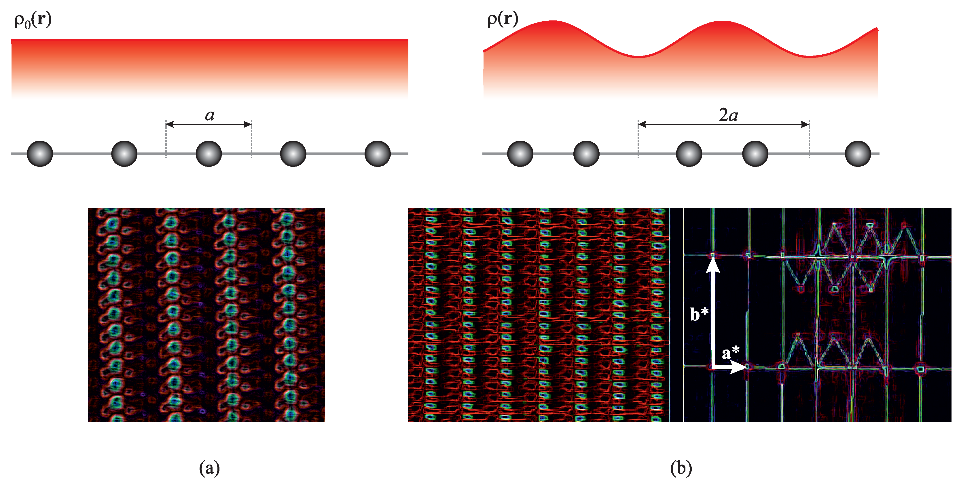
The magnitude of the gap parameter Δ , i.e., the order parameter of the CDW state, is stabilised by the deformation energy of the crystal lattice, proportional to its square. The non-vanishing mean value of phonon displacement operator b Q η + b Q η determines the displacement of atoms in the crystal lattice at position R n , m , i.e., d n , m = η A cos ( Q · R n , m ) . The amplitude of the displacement is A = a 0 Δ / g Q η , where a 0 is the amplitude of harmonic zero-point oscillations. Electron density is modulated accordingly, with respect to the initial homogeneous density, into a periodic structure following the deformation of the lattice. In the chain-like quasi-1D systems, it is a simple modulation along the chain with periodicity π / k F ; see Figure 8.
The presented mechanism of establishing the CDW ordering in 1D metal, mapped to quasi-1D nested systems, is known as the Peierls–Kohn instability. The results (25) reveal the remarkable property of systems with a perfectly nested Fermi surface: at zero temperature, the finite CDW order parameter appears even for arbitrarily small electron–phonon coupling. It is a direct consequence of the logarithmic term appearing in CDW condensation energy (24), which, in turn, originates from the fully gapped Fermi surface due to perfect nesting. An analogous type of behaviour is characteristic of the BCS superconductivity. It is a very important property of quasi-1D materials with highly isotropic, open Fermi surface, essentially distinguishing them from quasi-2D materials with closed and more or less isotropic Fermi surfaces to be elaborated in the section that follows. It should be stressed that what is presented in this section is the simplest picture of the onset of the CDW. The physics of real material, both experimentally and theoretically, is way more complex. For example, the CDW in TTF-TCNQ presented in Figure 8 (lower panel) is just the first one, after which at a lower critical temperature there follows a transition into the commensurate CDW phase driven by a double wave vector emerging due to the umklapp scattering [73,74]. All this complexity, now presented in a number of comprehensive reviews, is not the subject of this paper, serving merely to compare quasi-1D and quasi-2D basic mechanisms behind the CDW ordering.

4. Modern Concepts: Quasi-2D Systems

4.1. Materials

Typically, materials within the quasi-2D class are layered crystals with approximately isotropic properties in planes, but with strong anisotropy in the perpendicular direction, in terms of the TBA transfer integrals t x t y t z . In the metallic phase, the Fermi surface corresponding to the conducting plane is closed and more or less isotropic, depending on the symmetry of the crystal. In-plane conductivity is rather isotropic unless the material is some low-temperature ordered state, such as superconductivity, CDW, SDW, AF, etc. Some of the most well-known quasi-2D materials are as follows:
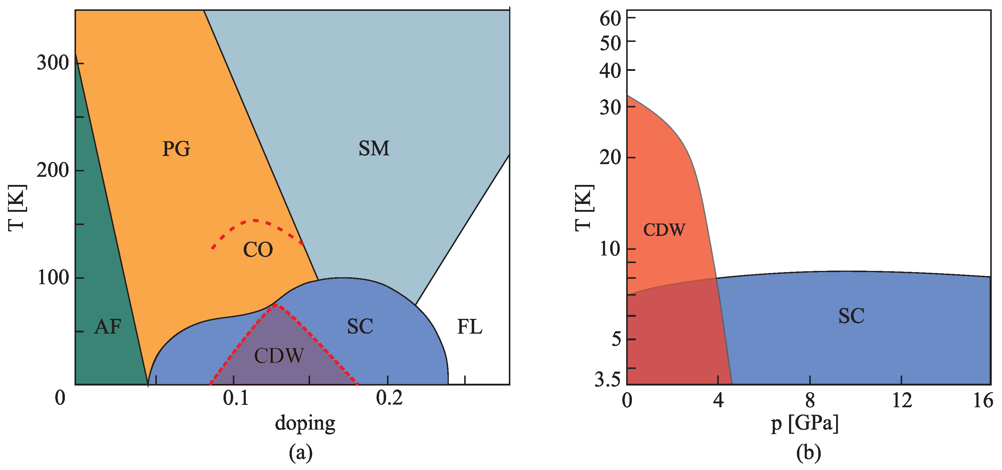
  • High-T c superconducting cuprates and related materials, e.g., YBa 2 Cu 3 O 7 p (“YBCO”), La 2 p Ba p CuO 4 (“LaSCO”), Bi 2 Sr 2 Ca 1 Cu 2 O 8 + p (“BSCCO”), HgBa 2 CaCu 2 O 6 + p (Hg-1212) and many others, where p determines stoichiometry that regulates amount of carrier doping, and thus the Fermi surface. The crystal structure of most of them is tetragonal (except YBCO, which is orthorhombic); see Figure 9a. Varying the stoichiometry of material by controlling amount of oxygen (p) in synthesis, copper–oxygen planes can be doped by holes or electrons resulting in an extremely rich phase diagram containing a vast number of phases among which charge ordering (different CDW phases) is the focus of this review; see Figure 10a. At zero-doping, the material is in an antiferromagnetic state due to band half-filling and perfect nesting of the square Fermi surface with Q = ( π , π ) wave vector. By doping, the nesting condition is deteriorated; the Fermi surface becomes a large, closed, hole-like pocket, almost circular; and other phases take place, i.e., superconductivity at lower temperatures and the so-called “pseudo-gap regime” above it. The pseudo-gap regime is characterised by a vastly reduced spectral function in the anti-nodal regions (i.e., ( π , 0 ) , ( 0 , π ) ) of the Fermi surface, leaving what resembles so-called “Fermi arcs” of high intensity around the nodal points ( k x , k y ) = ( ± k , ± k ) in ARPES spectra. Charge ordering appears within the pseudo-gap phase already at rather high critical temperatures of the order of 10 2 K, which is an order of magnitude higher than in weakly coupled quasi-1D materials, implying significantly stronger coupling responsible for it. Applying a strong magnetic field, on the order of several dozen Tesla perpendicular to the conducting plane, the “CDW dome” appears inside the SC phase where the charge ordering is significantly enhanced, gaining an-order-of magnitude-longer correlation lengths and even 3D ordering. A similar scenario is possible by doping the material with electrons, yielding an analogous but not a mirroring phase diagram.
  • Graphite intercalation compounds (GICs), with chemical formula XC n , are composed of graphite intercalated between the graphene layers comprising it, with alkali or alkaline earth metals X at each n carbon atoms ( n 6 ); see Figure 9b. The intercalation process yields a number of stable structures such as LiC 6 , CaC 6 , KC 8 , CsC 8 , etc, exhibiting interesting low-temperature superconductivity, and some of them a CDW phase at rather high critical temperatures on the order of 10 2 K. The intercalation of atoms between graphene layers, coupled by van der Waals interactions, increases the distance between layers and even inter-carbon distances inside them (e.g., in CaC 6 the interlayer distance is increased from 3.35 Å to 4.524 Å and the carbon–carbon distance from 1.42 Å to 1.444 Å). Charge transfer, taking place from metallic atoms to π -bands in graphene sheets, performs a chemical doping of carbon with electrons. It can attain high values compared to electrostatic doping and shift the Fermi energy by an order of electron volt, creating a well-developed Fermi surface in a metallic state of the material.
  • Transition metal dichalcogenides (TMDs) with chemical formula MX 2 , where M stands for transition metal (e.g., Mo, Ti, W, Nb, V) and X for chalcogen atom (e.g., S, Se, Te), form stable compounds that can be semiconducting (e.g., MoS 2 , WS 2 , MoSe 2 ) or metallic (e.g., TaS 2 , NbSe 2 ). In the context of this review, the metallic TMDs are more interesting since they can exhibit low-temperature superconducting or CDW ground states; see Figure 10b. Their crystal structure is layered, similar to that of graphite, where the MX 2 layers are coupled by van der Waals interactions, while the transition metal atoms within each monolayer are covalently bonded to chalcogen atoms from two layers sandwiching it in X-M-X structure; see Figure 9c. The Fermi surface in these materials is rather complex, in certain circumstances containing properties like saddle point or even partial nesting, rendering TMDs as materials very difficult for analytical analysis and requiring a comprehensive ab initio approach.
The shapes of the Fermi surface for three different quasi-2D materials are shown in Figure 11. They are very different from those in quasi-1D materials, definitely not perfectly, and in most cases not even partially nested, nevertheless, all these materials exhibit the CDW phase at a low enough temperature. In the section that follows, we set the minimal model looking for the very possibility and required conditions for establishing the CDW ground state in the Fermi surface configuration, fully excluding its nesting.

4.2. The Minimal Model of the CDW Transition in Quasi-2D Metal

Starting from the perspective of a weakly coupled 2D free electron gas and its zero-temperature susceptibility (see Figure 2), one cannot explain the onset of the Kohn anomaly due to the fact that the 2DEG susceptibility is a flat, featureless function for q ( 0 , 2 k F ) , unlike that in the 1D or quasi-1D nested systems. Susceptibility behaves this way if it is calculated in the model of rigid parabolic bands. This is not a realistic picture in real materials with rather strong electron–phonon coupling that alters electron bands. To address such processes and especially the finite temperature processes where anharmonicity effects start to play an important role, one would have to adopt the comprehensive ab initio approach. It is, however, possible to approach the problem analytically and grasp the qualitative description of the underlying CDW mechanism. The idea behind it is to self-consistently assume the existence of a finite CDW order parameter, calculate the CDW state condensation energy accordingly, and optimise it with respect to the new Fermi energy, the wave vector of the CDW potential and the order parameter itself. In modelling, we choose the zero-temperature case of rigid band yielding a closed, completely convex Fermi surface without any nesting features, to depict an “anti-nesting” regime and by that create “the worst possible scenario” for an order parameter should it exist at all. Any process of band modification then appears as a correction to the basic process of gap opening and Fermi surface reconstruction accordingly. The zero-temperature approach also makes the harmonic approximation in phonon description reasonable.
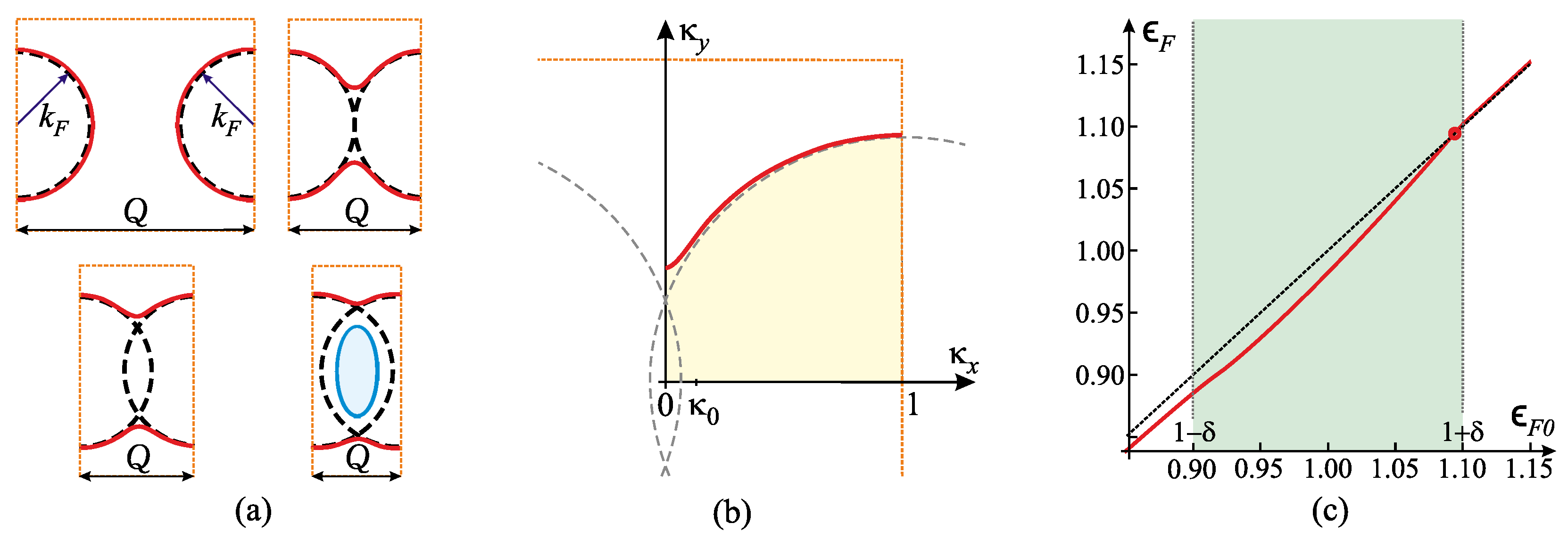
For the one-electron initial electron dispersion ε ( k ) in Equation (6), we choose the isotropic 2D free electron parabolic dispersion with circular Fermi surface, i.e., ε ( k ) = 2 | k | 2 / 2 m . The process of band reconstruction under the influence of self-consistent periodic potential created by the CDW with the wave vector Q = ( Q , 0 ) is illustrated in Figure 12.
Two bands are formed
E ± ( k ) = 2 2 m Q 2 4 + k x 2 + k y 2 ± ( Q k x ) 2 + 2 m Δ 2 2
with hyperbolic point at energy ε H in the lower band, and elliptic point at energy ε E in the upper band. The existence of a hyperbolic point in the lower band will turn out to be crucial for the stabilisation of the CDW ground state, particularly due to the fact that it is self-consistently created by the CDW potential. The region of energy, 2 Δ -wide between ε H and ε E , we refer to as the pseudo-gap, as we shall elaborate later (to be distinguished from the pseudo-gap often used in the field of high-T c superconductors).
Optimisation procedure in the self-consistent process of band reconstruction is performed with respect to wave vectors Q , which determine the overlap of the Fermi surfaces and the size of the new Brillouin zone (see Figure 12), order parameter Δ that acts as a gap parameter and Fermi energy of the reconstructed system ε F which can in principle change with respect to the initial Fermi energy ε F 0 . Optimisation is carried out under the constraint that the number of electrons before and after the band reconstruction is conserved, i.e., N 0 ( ε F 0 ) = N ( ε F ) . Number of electrons in the band, up to energy ε at zero temperature, is N ( ε ) = 0 ε g ( ε ) d ε = V 2 π 2 S ( ε ) , where g ( ε ) represents an energy-dependent density of states (DOS) of the system, either initial g g 0 , or reconstructed g g , and S ( ε ) is an area of reciprocal space enclosed by the contour of constant energy ϵ ( k ) = ε , either initial S S 0 , or reconstructed S S (see Figure 12). In the same manner, the zero temperature energy of electron band up to the one-electron energy ε is E b a n d ( ε ) = 0 ε ε g ( ε ) d ε = ε N ( ε ) V 2 π 2 0 ε S ( ε ) d ε , using integration by parts and assuming the relation g ( ε ) = d N ( ε ) / d ε . Then, the relation (10) for the zero-temperature CDW condensation energy can be expressed as
E CDW = ε F 0 N 0 ( ε F 0 ) ε F N ( ε F ) + V 2 π 2 0 ε F S ( ε ) d ε 0 ε F 0 S 0 ( ε ) d ε E l a t t .
In the first step, we optimise E CDW with respect to ε F and Q, keeping Δ fixed and to be optimised in the second step. Although present implicitly in choosing the phonon mode at the wave vector Q , we assume the Q -dependence of the coupling constant g Q η as well as of Δ to be slow enough to be neglected in the optimisation procedure (by that also excluding E l a t t from the first step of optimisation). Taking into account the particle number conservation constraint, we define the Lagrange function L = E CDW μ Δ N , where μ is the Lagrange multiplier and Δ N N ( ε F ) N 0 ( ε F 0 ) . Performing the standard optimisation procedure, we obtain the following three conditions:
( 1 . ) 0 = L ε F 0 = g 0 ( ε F 0 ) ( ε F 0 μ ) ( 2 . ) 0 = L ε F = g ( ε F ) ( μ ε F ) ( 3 . ) 0 = L Q = 0 ε F S ( ε , Q ) Q d ε .
System (28) yields the optimal value of the Fermi energy of the reconstructed system
ε F = ε F 0
being equal to the initial value as long as there is Q = Q o p t for which S ( ε F , Q ) has a maximum. It happens if this maximum is achieved in the lower band before the upper band starts to get filled (filling of the upper band immediately cancels all band energy changes due to reconstruction). In the process of reconstruction, the initial Fermi surfaces start to increasingly overlap as Q is reduced from large (larger than 2 k F ) to smaller values. The enclosed area S ( Q ) is first unchanged before there is an overlap and lifting of degeneracy, and then it starts to increase because of the finite gap parameter Δ and lifting of degeneracy due to the overlap, and then it starts to decrease due to the sole fact that the size of the Brillouin zone ( Q / 2 , Q / 2 ) is reduced by the reduction in Q (see Figure 13a). If a maximum is achieved in the lower band before the filling of the upper one, then it happens at energy ε F = ε F 0 . If the maximum is not reached before the upper band starts to get filled, then the reduction in Q stops there and the new Fermi energy remains lower than initial, i.e., ε F < ε F 0 [53,54,55].
The optimal value of the CDW wave vector, Q o p t , is determined from the condition of particle number conservation and Equation (29), which reduces to
S 0 ( ε F ) = S ( ε F , Q , Δ ) | Q = Q o p t ,
where S 0 ( ε F ) = 2 π m ε F / 2 . The reconstructed area is calculated by integration S ( ε F , Q , Δ ) = 4 0 Q / 2 k y ( k x ; E , Q , Δ ) | E = ε F d k x , where k y ( k x ; E , Q , Δ ) is easily found from Equation (26) taking into account the lower band, i.e., E ( k ) . As the integral cannot be taken in a closed form, for the purpose of an analytical approach, the special technique of controlled expansion is developed to evaluate it [53,55]. First, we put Q in scale with momentum and energy variables, i.e., we define them as
κ x , y k x , y Q / 2 , ϵ E ε Q , δ Δ ε Q ,
where ε Q 2 ( Q / 2 ) 2 / 2 m , and define an arbitrary scale κ 0 under condition δ κ 0 1 with respect to which we perform expansion of (scaled) expression k y ( k x ; E , Q , Δ ) (see Figure 13b), i.e.,
κ y < ( κ x ; ϵ , δ ) = ϵ 1 κ x 2 + 4 κ x 2 + δ 2 , κ x ( 0 , κ 0 ) κ y > ( κ x ; ϵ , δ ) = ϵ ( 1 κ x ) 2 + δ 2 8 κ x ϵ ( 1 κ x ) 2 , κ x ( κ 0 , 1 ) .
In terms of expressions (32), Equation (30) reads
π 4 ϵ F = 0 κ 0 κ y < ( κ x ; ϵ F , δ ) d κ x + κ 0 1 κ y > ( κ x ; ϵ F , δ ) d κ x .
In the second step, we define
ϵ F = 1 + δ + ζ ( δ ) δ
where ζ ( δ ) is a function to be determined, by assumption small, of the order δ > 1 , and expand integrals in Equation (33) in terms of ζ . The validity and order of expansion are controlled by asymptotic matching of terms containing the scale κ 0 from the upper limit of the first and the lower limit of the second integral, which must cancel each other up to the required order. The procedure yields the first non-vanishing contribution ζ ( δ ) = 1 2 π δ . Using the scaling relations (31), we find Q = 2 k F / ϵ F which, using Equation (34), directly yields the optimal CDW wave vector
Q o p t 2 k F 1 1 2 Δ ε F + 1 2 2 π Δ ε F 3 2 .
Correction to 1 in the square bracket of expression (35) determines an optimal overlap of initial Fermi surfaces in the process of the reconstruction with respect to touching of the Fermi pockets (i.e., Q = 2 k F is the value at which they exactly touch, while Q o p t < 2 k F ).
The zero-temperature condensation energy is calculated from Equation (10), using Equation (8) for the lower band (26), where
E b a n d Δ = 0 = 1 2 g F 2 D ε F 2 E 0
and
E b a n d Δ 0 = V 2 π 2 4 0 Q 2 d k x 0 k y F ( k x ; Q , Δ ) d k y E k x , k y ; Q , Δ | Q = Q o p t ε F = ε F 0 ,
with k y F ( k x ; Q , Δ ) k y ( k x ; ε F , Q , Δ ) denoting integration up to the Fermi energy (see Figure 13b). As the closed-form analytical result is not feasible, the strategy to extract terms that govern stabilisation of the CDW state is to use convenient expansions. Since the lattice term is ∼ Δ 2 , we expect that criticality, i.e., the instability of initial ground state, is determined by the electron band terms up to and of that order in Δ , while the first non-vanishing contribution ∼ Δ > 2 of the opposite sign provides compensation that stabilizes the CDW ground state, determining its order parameter. Using the scaling of variables (31), the band energy can be expressed as E b a n d Δ 0 = 2 π E 0 q 0 4 I | o p t , where q 0 Q / ( 2 k F 0 ) | Q o p t defined in Equation (35), and
I 4 0 1 d κ x 0 κ y F ( κ x ; δ ) d κ y ϵ ( κ x , κ y ; δ ) ,
in which we use scaled Equation (26) for the lower band
ϵ ( κ ) = 1 + κ x 2 + κ y 2 4 κ x 2 + δ 2 .
Analytical evaluation of integral I , being impossible directly, is carried out by evaluating its total derivative
d I d δ | o p t = I ϵ F ϵ F δ + I δ | o p t = π 2 ϵ F 0 2 δ 4 δ J ( δ ) ,
where we define
J 0 1 d κ x κ y F ( κ x ; δ ) 4 κ x 2 + δ 2 .
Terms in Equation (40) were evaluated straightforwardly, i.e., ϵ F I = 4 0 1 d κ x ϵ F κ y F ϵ ( κ x ; κ y F , δ ) = ϵ F ϵ F 4 0 1 d κ x κ y F ( κ x ; δ ) , using 4 0 1 d κ x κ y F ( x ; δ ) = π ϵ F 0 = π ϵ F by virtue of Equations (30) and (29). The number of particles with nullified terms where that integral had appeared under the derivative with respect to δ was conserved. Terms in I , containing required powers of δ , are calculated by formal integration of expression (40) obtained through appropriate expansions in terms of δ . The first term cancels the contribution of the initial unordered state, while the second term accounts for the gain in the CDW condensation energy due to band modifications introduced by the finite order parameter. Integral (41) is evaluated in terms of controlled expansions, using Equation (32) for κ y F ( κ x ; δ ) in the analogous way as Q o p t , yielding J = ( 2 + π ) / 4 δ / π + . It is evident that, after formal integration of Equation (40) with respect to δ , the zeroth order ∼ δ 0 in expansion of J yields the instability term ∼ δ 2 in E CDW , while the first non-vanishing one of opposite sign ∼ δ 1 stabilizes E CDW with term ∼ δ 3 . Collecting all the terms and returning from scaled to original variables, i.e., ϵ F = q 0 2 , δ = ( Δ / ε F ) q 0 2 , we evaluate the CDW condensation energy Equation (10) up to the third order in Δ to
E CDW E 0 = 1 + 2 π 1 λ Δ ε F 2 1 π Δ ε F 3 .
The coefficient appearing with Δ 3 has the proper sign to stabilise CDW, i.e., expansion up to the cubic term in Δ is sufficient to describe the basic physical picture. The straightforward optimization of condensation energy (42) with respect to order parameter Δ yields an equation
Δ 1 + 2 π 1 λ 3 π ε F Δ = 0 .
It describes a bifurcation with a change in stability between two solutions, Δ = 0 and Δ 0 , depending on the sign of the term 1 + 2 / π 1 / λ , i.e.,
Δ = 0 , λ < λ c 2 π 3 1 λ c 1 λ ε F , λ > λ c
where
λ c 1 + 2 π 1 0.611 .
The quantity λ c 0.611 is the critical electron–phonon coupling for a phonon mode ω Q η required to stabilise the CDW ground state [53]. The stable zero-temperature CDW state appears through a bifurcation, in a sense a quantum transition of the Lifshitz type on a domain of the coupling strength, when electron–phonon coupling λ exceeds the critical value λ c , with the emerging order parameter Δ ( λ λ c ) ε F close to the critical point. The result is shown in Figure 14a. Numerical analysis, taking into account the effective dimensionality of the metallic system with the free electron parabolic dispersion, shows that λ c monotonically increases from zero in the case of 1D system (effectively the case of perfect nesting) to the 3D value on the order of one (see Figure 14b) [54]. Corresponding condensation energy (42) for optimal order parameter (44) in the 2D system is E CDW = 4 π 2 27 E 0 1 λ c 1 λ 3 .
Calculating the area S ( ε , Q , Δ ) directly allows the electron DOS to be calculated, i.e., g ( E ) = V 2 π 2 d S ( E ) / d E . The result, taking into account both bands, E and E + , is presented in Figure 14c. It is easily shown that at the energy of the hyperbolic point ε H in the lower band, the main value of the integral indicates a logarithmic type of van Hove singularity, while at the energy of the elliptic point ε E in the upper band, the system develops a Heaviside step. Fermi energy is optimally positioned inside the pseudo-gap between ε H and ε E . Electron states inside the pseudo-gap are depleted and “pushed” to lower energies into the van Hove singularity. Since the very creation of such van Hove singularity below the Fermi energy is self-consistent, it has a profound effect on electron properties of the system, particularly the CDW condensation energy and, as we show in what follows for the particular material, leads to stabilisation of the CDW ground state.

4.3. Test of the Model: The CDW Ground State in CaC 6

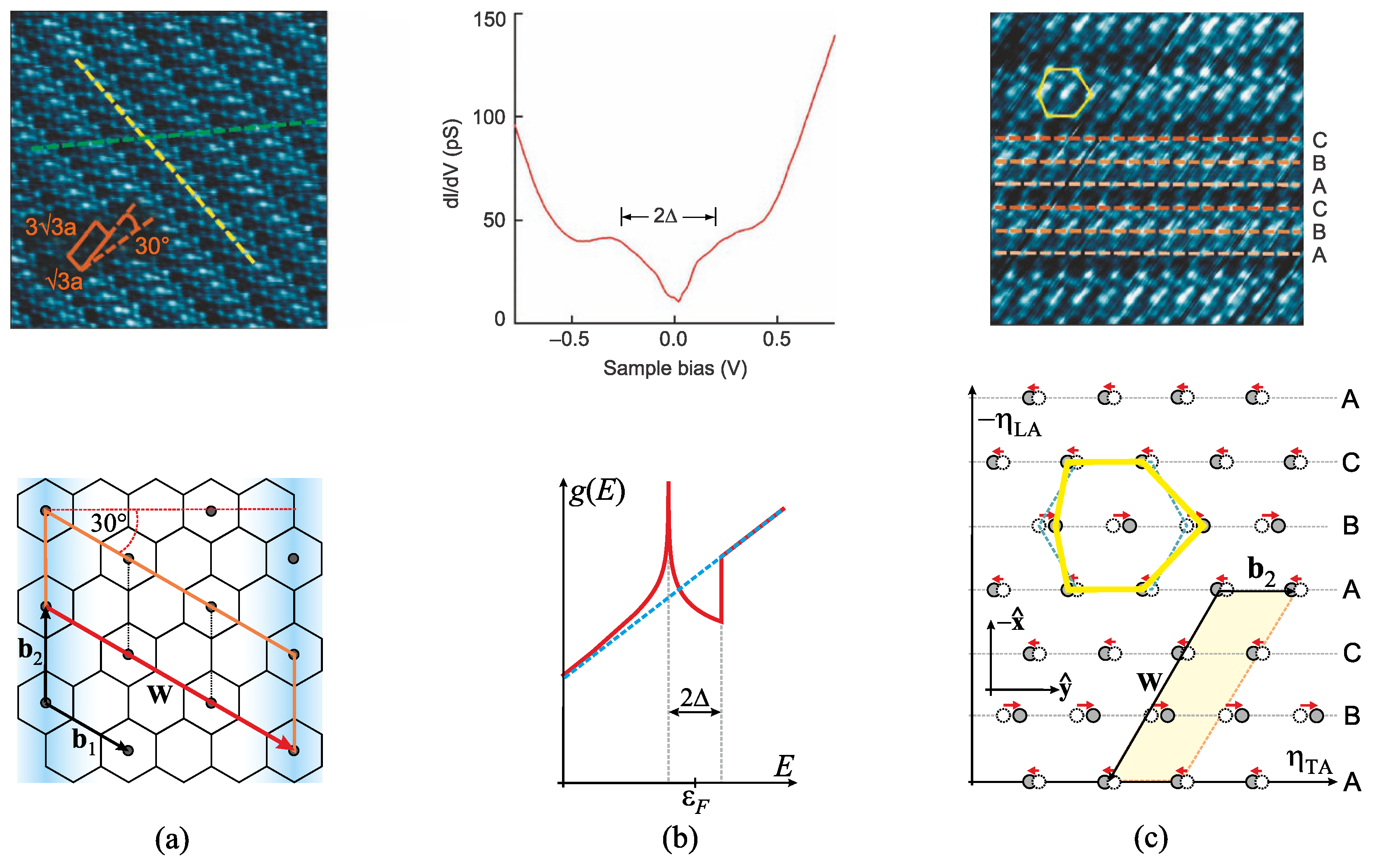
The intercalated graphite CaC 6 represents a perfect example system to check the model proposed in the previous section, due to the set of experimental data that exactly pinpoints key steps in the onset of the CDW ground state. At the same time, it does not exhibit such complexity of the relevant Fermi surface and corresponding bands, such as in the case of TMDs, for example, avoiding additional effects that can be addressed only numerically. In this section, we demonstrate explaining the following key findings in the experiment performed by Rahnejat et al. [35] by the considered analytical model: (1) The uniaxial CDW ordering is established in the graphene sheets that are chemically doped by electrons from the Ca atoms with 0.2 electrons per carbon atom into the π -band. The CDW formation triples the CaC 6 unit cell along one of its primitive vectors inclined by 60 degrees to the crests of the CDW (30 degrees with respect to the CDW wave vector). The charge lines (CDW crests) are formed along the graphene armchair direction, with a distance between them equal to 4.5 graphene lattice constants along the graphene zig-zag direction. (2) The pseudo-gap in electron DOS is formed around the Fermi surface in the CDW-ordered phase. (3) The Ca superlattice is deformed in a specific way: the line of Ca atoms “under” the CDW crest is shifted by 0.06 ± 0.02 nm along the crest direction, with respect to two parallel lines of Ca atoms between the crests. The analytical procedure is elaborated in detail in Ref. [55]. The calculation of the critical temperature, here T c 250 K, is not within the scope of this model due to reasons stated in the next section.
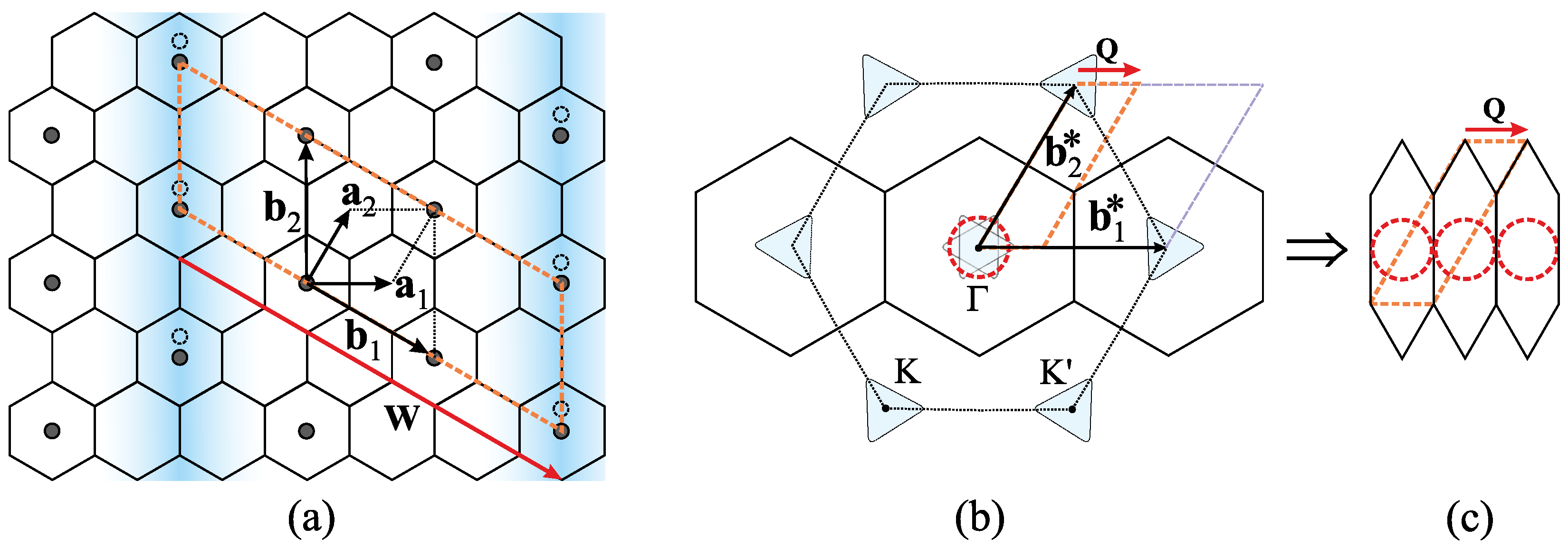
The geometry of the problem, approximated from quasi-2D to 2D real and reciprocal space, is presented schematically in Figure 15.
The technical difference with respect to the model presented in the previous section is linear initial electron dispersion instead of parabolic, i.e., ε ( k ) = v F | k | , which leads to some qualitative and mostly quantitative differences. The initial electron DOS in a metallic state is in this case linear in energy, i.e., g 0 ( E ) = 6 V π 2 v F 2 E . Linearity of initial electron dispersion does not permit obtaining a simple closed form of k y ( k x ; E , Q , Δ ) dependence, but its expansions in terms of scaled variables (31) can be obtained analytically
κ y < ( κ x ; ϵ , δ ) = 2 ϵ 1 + 4 κ x 2 + δ 2 , κ x ( 0 , κ 0 ) κ y > ( κ x ; ϵ , δ ) = ϵ 2 ( 1 κ x ) 2 1 + 1 + 4 κ x 4 κ x 2 2 κ x δ 2 , κ x ( κ 0 , 1 )
where ε Q v F ( Q / 2 ) has been used in scaling the energy variables. Additional difference is that in summation (8) to yield the band energy, now, besides spin (factor 2), we have additional degeneracies, i.e., valley (factor 2) and tripling the unit cell due to the Ca-superstructure (factor 3), yielding in total factor 12 instead of 2 in front of the summation over k . Equation (30) for conservation of particle number, which yields optimal CDW wave vector and Fermi energy, now reads
ε F 2 ε F 0 2 = 2 v F Q 2 ε F v F Q 2 + Δ ε F v F Q 2 Δ α π Δ 2 ,
where α = 0.5568 . This equation demonstrates an example of system that would, at ε F = ε F 0 , have Q < Q E 2 ( ε F 0 Δ ) / ( v F ) which corresponds to energies E > ε E , i.e., the upper band would have been filled. It therefore determines the reconstruction wave vector stopping at the value Q E and Fermi energy of the reconstructed system lower than the initial, ε F < ε F 0 , i.e.,
Q o p t = 2 k F 1 Δ ε F 0 , ε F = ε F 0 1 α 2 π Δ ε F 0 2 .
Using values (48) and using the previously elaborated technique of controlled expansion, we obtain the CDW condensation energy
E C D W E 0 = 3 2 1 λ c 1 λ Δ ε F 0 2 3 β 2 π Δ ε F 0 3 ,
where β = 5.578 . Here,
λ c π α 3 + β 1 0.54
appears to be the critical value of the electron–phonon coupling constant.
As it is seen from the result, | b 1 , 2 | 3 · 2 k F , i.e., the 2 k F 0.56 Å 1 is commensurate with the reciprocal lattice constant b 1.68 Å 1 by factor 3. It means that stabilising the CDW with wave vector Q o p t from Equation (48), having (although small) correction from the 2 k F value, would in principle lead to the incommensurability effects between periodicity of the CDW and the underlying lattice. A comprehensive analysis of those effects represents a formidable and important task which is beyond this basic model. Roughly, we may say that in this class of materials, such an incommensurability generally leads to a decrease in the order parameter, reduction in correlation length, the formation of domains, and other deteriorating effects on the CDW, visible in cuprates by the change in doping and in TMDs by pressure and intercalation [82,83,84,85,86,87]. Competition between commensurability and incommensurability is even more subtle in quasi-1D materials, involving the important role of the umklapp scattering and other effects related to anomalous dimensionality close to 1D. In most cases, the low-temperature phase is commensurate; thus, in what follows, we shall neglect this competition, assuming that the wave vector of the CDW ordering attains the commensurate value, i.e., Q = 1 3 b 1 * , which places the Fermi energy in the middle of the pseudo-gap.
The phonon mode that is softened, responsible for the onset of the CDW, is the one at the wave vector Q , with the maximal value of electron–phonon coupling λ to self-consistently maximise the order parameter Δ and correspondingly the E CDW . This mode, with maximal value of (dimensionless) electron–phonon coupling (7), λ Q η g Q η / ω Q η , is apparently one at polarisation η with maximal coupling g Q η and minimal frequency ω Q η at the wave vector Q , to maximise their ratio. To identify such a mode, it turns to numbers either from experimental data or comprehensive momentum-resolved ab initio studies of electron–phonon coupling, which are quite rare compared to those providing the cumulative or average value over momenta. Among number of ab initio studies [88,89,90,91,92,93,94], some address the soft in-plane vibrations of calcium superlattice Ca x y at ∼ 10 meV compared to order of magnitude harder carbon lattice vibrations at ∼ 100 meV [93,94]. Also, a significant value of very anisotropic electron–phonon coupling between carbon electrons and Ca-phonons is indicative in the vicinity of the M point in the CaC 6 Brillouin zone [90], which is exactly where the experimentally observed CDW wave vector is placed. This is quite enough motivation to investigate the possibility of an in-plane Ca-phonon as responsible for the CDW instability.
Vibrational modes of the 2D Ca lattice are described within the harmonic first-neighbour approximation. The in-plane atom displacement d n m from the equilibrium position at R n m is described by the equation
M d 2 d t 2 d n m = K i = 1 3 2 d ( R n m ) d ( R n m + b v i ) d ( R n m b v i ) · v i v i ,
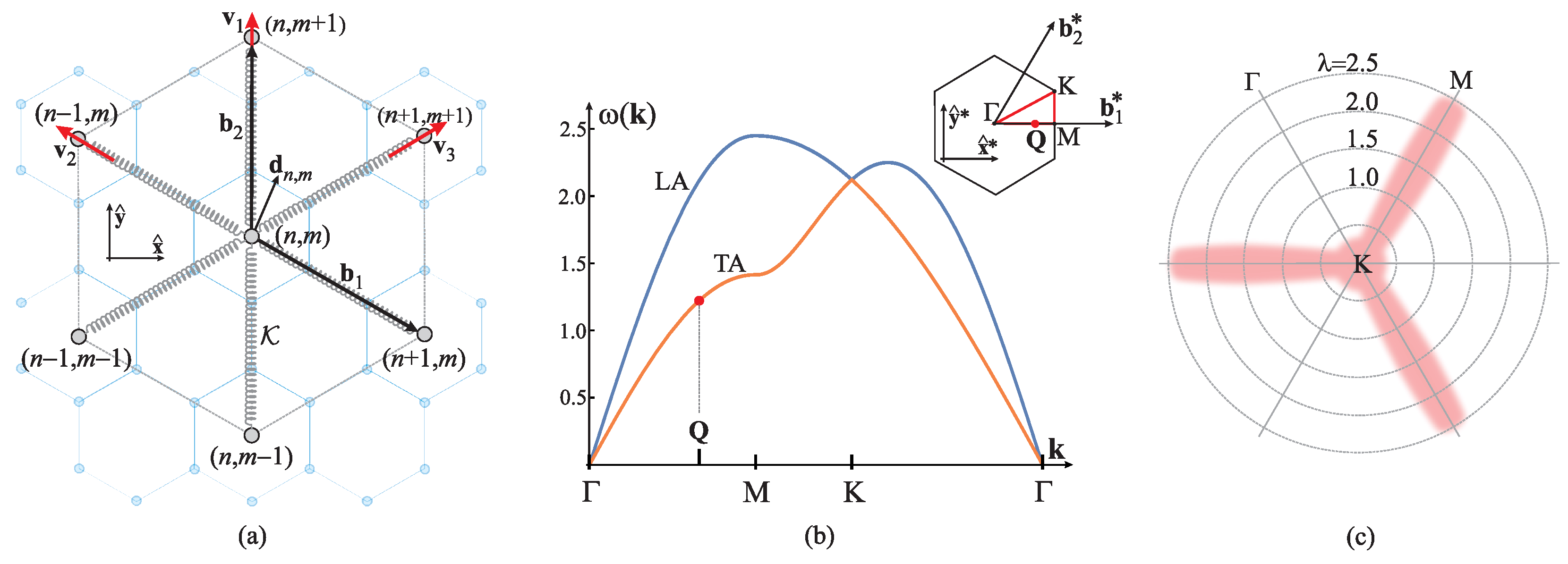
where M is the mass of the Ca atom, K is the linear elasticity constant, b is the lattice constant (Ca-Ca interatomic distance), while v i , i = 1 , 2 , 3 , are the unit vectors along three characteristic directions of motion for the hexagonal symmetry (see Figure 16a).
Assuming a solution of Equation (51) in the standard form, i.e., d n m = η exp i [ k · R n m ω t ] , where k is the wave vector, ω is the frequency and η = ( η x , η y ) is the polarisation vector of the phonon mode, Equation (51) reduces to the secular equation
3 K M 1 h 1 ( k ) ω 2 3 K M h 2 ( k ) 3 K M h 2 ( k ) K M 3 h 1 ( k ) 2 h 3 ( k ) ω 2 η x η y = 0 ,
where h 1 ( k ) cos ( 3 2 k x b ) cos ( 1 2 k y b ) , h 2 ( k ) sin ( 3 2 k x b ) sin ( 1 2 k y b ) , h 3 ( k ) cos ( k y b ) . It yields the dispersion relation of phonon modes
ω ± ( k ) = K M 3 2 h 1 ( k ) h 3 ( k ) ± ( h 1 ( k ) h 3 ( k ) ) 2 + 3 h 2 ( k ) 2 1 2
(see Figure 16b). At the CDW wave vector Q = 1 3 b 1 * , Equation (53) yields two frequencies, ω = 3 K / 2 M and ω + = 9 K / 2 M , and, by virtue of Equation (52), the corresponding polarisation unit vectors η = ( 0 , 1 ) y ^ (TA) and η + = ( 1 , 0 ) x ^ (LA), respectively. The TA mode apparently has a lower frequency (red dot in Figure 16b). Since the coupling g originates from the modification of electron–ion potential due to the ionic shift caused by the phonon, in the spirit of the TBA [95,96,97,98] it is g R R t ( R R ) · η , where t ( R R ) is the TBA transfer integral of electron hopping between atoms at positions R and R within the first neighbour approximation. The Ca atom is centred below the carbon hexagon (see Figure 16a) thus all t are equal, but the sum of their projections along the TA exceeds the sum along the LA direction yielding g T A > g L A . The shift of Ca along the TA direction “strikes” directly into the neighbouring atomic orbital, which is not the case in the LA direction, being the main cause of this difference. Both of these insights yield the conclusion that the dimensionless coupling λ g 2 / ω Q is λ T A > λ L A and hence the TA mode induces the CDW instability. Numerical insight on CaC 6 [90] indicates hybridisation of Ca and carbon bands and very anisotropic ARPES electron–phonon coupling, rather pronounced, up to the value of 2.5, along the K-M direction in the CaC 6 Brillouin zone (see Figure 16c). The strength of the coupling in the vicinity of the M point, where Q resides, should be larger than 0.54 within the minimal model presented here. Deformation of the Ca lattice, i.e., displacements of atoms d n m = η T A cos [ Q · R n m ] that corresponds to such polarisation and periodicity, occurs in a way that atoms along the CDW crests (each 4th column along y ^ -direction) are displaced by η T A while all others are displaced by 1 2 η T A in terms of amplitude d = | η T A | which is proportional to the order parameter Δ . The amplitude is determined by the mean value of a phonon displacement operator a 0 ( b Q + b Q ) , where a 0 is the amplitude of zero-point oscillations, i.e., d = 2 b Q a 0 = a 0 Δ / g Q . Figure 17 shows a comparison of the results obtained in the experiment (upper panel) and prediction of the model (lower panel), exactly matching the direction and periodicity of the CDW, formation of the pseudo-gap around the Fermi energy and characteristic deformation of the Ca-lattice with respect to the CDW.

4.4. And Beyond Analytics

The real materials, naturally, deviate from the minimal model in many aspects, among which some can be approximated analytically up to a sufficient degree, and some simply cannot. For example, the appearance of many bands at the Fermi level in real materials, such as CaC 6 that we considered in the previous section [88,89,90,91,93,99], can be addressed within the minimal model by eliminating most of them from the critical phenomenon due to the sole fact that they do not fulfil the “Fermi surface size vs. the CDW wave vector requirement”, i.e., that the Fermi pockets should be related by Q in a particular way to form a chain of slightly overlapping pockets to open a pseudo-gap and place the Fermi energy inside it, without filling the upper band (too large overlap) that would cancel out the effect. Also, some deviations of the band structure from the model can be neglected if they are sufficiently far away from the Fermi surface, for example, the existence of the small gap on the bottom of the CaC 6 band instead of the Dirac point, since they cancel out in the condensation energy calculation anyway. However, such band details may have decisive effects if they are close to the Fermi energy. Also, the rigid band approximation is by all means not precise enough in the strongly coupled systems, modifying the band sometimes significantly, which can be of utmost importance close to degeneracies, such as the flat susceptibility of the 2DEG with rigid parabolic band (Figure 2b). Furthermore, in contrast to the weakly coupled systems, which require nesting to acquire the ordered ground state for which the critical temperature can be obtained to satisfactory precision from a rather simple finite-temperature and rigid band susceptibility analysis, for strongly coupled systems, the analogous procedure is not satisfactory. In particular, just calculating the energy of the reconstructed band Equation (8) integrating over the Fermi function would not be sufficient to grasp all important aspects of both electron and phonon dynamics and would at best give an estimation of the order of magnitude of the transition critical temperature to the CDW state. Since the CDW transition critical temperatures of the strongly coupled systems (cuprates, TMDs, GICs etc.) are, in general, an order of magnitude higher compared to the weakly coupled systems (Bechgaard salts, blue bronze etc.), i.e., of the order of 10 2 K, two important contributions need to be accounted for: the entropy contribution in the free energy both from electrons and phonons, and the anharmonicity effects of lattice dynamics. Both, the high-entropy disordered state and stiffening of phonon modes by anharmonicity of the potential, are in competition with the condensation energy gain due to the electron band reconstruction and can significantly affect the CDW transition temperature. The transition becomes of the first order with an abrupt jump, in contrast to the continuous second-order transition related to the harmonic approximation. In some systems, it has even been observed that the coupled phonon mode does not soften entirely down to zero due to anharmonic stiffening, drastically lowering the critical temperature or even preventing the CDW from stabilising at all. Considering the anisotropy of this class of materials inclined to two-dimensionality, one can expect the mentioned effects to be even more pronounced due to the appearance of van Hove singularities and natural softness of lattice vibrations, as well as anisotropy of their coupling to electrons. Two well-known and studied examples among TMDs are 2H-NbSe 2 and 2H-TaSe 2 . The occurrence of CDW in TMDs is particularly demanding to explain due to, in addition to all counted, rather complex Fermi surface containing saddle points (see e.g., Figure 11) that simply lure to an attempt to fit them to some aspect of nesting mechanism. As mentioned in the Introduction, to make the Kohn anomaly criterion (12) more realistic, it was supplemented with lattice-related contributions such as electron Coulomb ( U q ) and exchange ( V q ) energies, i.e.,
4 g q 2 ω q + 2 U q V q 2 χ q ,
where χ q is defined by expression (13) [43,44], or, besides the standard polarisation (“bubble”) diagram, taking into account anharmonic cubic and quartic phonon self-energy contributions [45] (see Figure 18). Such studies paved the way to the nowadays well-accepted ab initio approaches relying on strong electron–phonon coupling, essentially momentum dependent, with no necessity for the Fermi surface nesting, i.e., for the singular behaviour of electron susceptibility [100,101].
The example of the aforementioned incomplete phonon softening is 2H-NbSe 2 , where at the CDW transition temperature of 33 K the phonon mode softens at the wave vector Q CDW not to zero, but to small finite-frequency value, in the first order transition due to anharmonic lattice stiffening and thermal fluctuations [102,103]. The phonon softening in the Kohn anomaly occurs not so sharply as in the nesting-driven systems, but forms a rather wide cusp around the point Q CDW in the momentum domain as a consequence of phonon fluctuations localised in real space. Following the idea from Ref. [45], supplementing the RPA equations with strong momentum-dependent electron–phonon interaction and taking into account the anharmonic phonon mode-mode coupling approximation (MMA), reproduces the occurrence of the pseudo-gap in accordance with experiment [104], as well as the observed softening of phonon mode at Q CDW = 0.98 2 3 Q Γ M and critical temperature of 33.5 K, roughly an order of magnitude lower than that predicted by standard RPA [105]; see Figure 19.
Those and alike effects beyond linear models, in most cases crucially depending on the material-specific details, can be grasped only by the comprehensive ab initio approaches, nowadays the most popular among them being based on the density functional theory (DFT); see for example Refs. [56,57,58,59,89,91,93]. The most well-known software packages used by many research groups worldwide to study the CDW ground state are the combination of: Quantum ESPRESSO or VASP for the electron band structures and material simulations, Phonopy for the crystal lattice dynamics in terms of phonon modes, with all aiding tools for Wannier orbitals construction, handling of molecular dynamics etc. A detailed overview of these techniques is way beyond the scope of this review, focused on relating Fermi surface nesting and basic “beyond nesting” mechanisms. The ab initio studies are the basis for the material-specific results describing the CDW ground state already at the industrial standard of accuracy, as well as for its engineering by ultrafast light pulses or strain, which are in focus of modern, cutting-edge CDW-oriented research [106,107,108,109].

5. Conclusions

The field of charge density waves has been actively evolving for almost five decades now. Encouraged by the essentially one-dimensional model of Peierls instability from the thirties of the last century, the predominant initial direction of experimental and theoretical research was focused on alike systems and real materials with highly anisotropic quasi-1D structure. In those systems with rather weak electron–phonon coupling and transition temperatures of the order of 1–10 K, nesting of Fermi surface sheets, of open geometry due to unit cell anisotropy, has been the key mechanism of the instability of metallic state of the system and stabilisation of the CDW ground state (or SDW depending on the nature of interactions). A number of methods have been developed to control imperfections in the Fermi sheets nesting, whether by hydrostatic pressure, which increases them, affecting the TBA transfer integrals, or by strong external magnetic field that effectively removes them through the mechanism of Landau quantisation of the “nesting imperfection pockets” formed on the Fermi surface. Either way, the ground state of such systems is very sensitive to tapping into the underlying nesting and results in a sequence of phase transitions between different phases of broken symmetry (SP, AF, SDW, CDW, SC) in the first case, or a cascade of SDW or CDW field-induced phases in the second case, respectively. The signature of the perfectly nested system is a characteristic term in the CDW condensation energy, with logarithmic dependence on the order parameter, that at zero temperature provides a finite order parameter even for infinitesimally small electron–phonon coupling. The theory and experiment sealed a perfect marriage in these systems, materials like Bechgaard salts, transition metal bronzes, transition metal trichalcogenides and others, providing an understanding of practically the whole phase diagram with embedded details.
Contrasted to them are the quasi-2D systems, consisting of conductive layers with Fermi pockets of closed geometry, in most cases far away from any form of nesting. Yet, they exhibit a CDW ground state with transition temperatures of the order of 10–102 K, as observed in materials like high-T c superconductors, intercalated graphite compounds, transition metal dichalcogenides and others. It is the main message of this focused review to address the change of the nesting paradigm from the weakly coupled quasi-1D nested systems to quasi-2D strongly coupled systems that show no property of nesting. In that respect, we elaborate the minimal zero-temperature model of the “worst possible scenario” comprising the circular Fermi pockets, in the entirely anti-nesting configuration, which yields the CDW ground state if strong enough electron–phonon coupling to a soft phonon mode is provided by the system. The transition is Lifshitz-like, based on topological reconstruction of the Fermi surface from closed to open geometry. The self-consistent, periodic CDW potential relates closed Fermi pockets into a slight overlap, so that a hyperbolic point is formed in the energy spectrum. It leads to the self-consistent formation of the pseudo-gap around the Fermi energy, and a logarithmic van Hove singularity on its lower edge, below the Fermi energy. In that way, the electrons, through interaction with phonons, self-redistribute from the states depleted by the pseudo-gap to the lower energy states inside the created van Hove singularity, consequently lowering the total band energy. This negative gain in electron band energy is to overcome an increase in elastic energy of the crystal lattice deformed by the “frozen” phonon mode, which depends on electron–phonon coupling. Their exact balance determines a critical value of the coupling constant, required to be exceeded to gain a finite condensation energy to stabilise the CDW state. Here, one sees the basic difference between the perfectly nested systems, where the Fermi surface is fully gapped providing the zero-temperature CDW order parameter even for arbitrarily small coupling, and non-nested systems where the finite order parameter appears through the Fermi surface reconstruction and formation of the pseudo-gap with van Hove singularity below if coupling is larger than critical. The Fermi surface in the latter primarily acts through its size (in contrast to the first ones in which its shape is essential) since the softened phonon mode needs to provide a CDW vector of such periodicity and direction that preferably relates the Fermi pockets into a chain of optimally overlapping pockets, commensurate with the reciprocal lattice, or very close to it. Besides insufficient coupling, that is one of the main reasons why most metallic materials do not exhibit a CDW ground state. Since the CDW order parameter is directly proportional to the dimensionless electron–phonon coupling constant, it is self-consistently maximised by choosing the phonon mode with the strongest coupling to electrons and minimal frequency (for which the in-plane vibrations inside the quasi-2D systems are especially suitable), at CDW wave vector and polarisation that relates the Fermi pockets and reconstructs the Fermi surface in the optimal way. Even on the level of a minimal model, the onset of the CDW in the intercalated graphite compound CaC 6 , its periodicity and direction, as well as static distortion of the crystal lattice, can be understood.
The deeper understanding beyond the qualitative picture, the strong, momentum-dependent electron–phonon coupling and finite temperature, material-specific effects, requires more sophisticated methods. Namely, instead of the rigid bands, one needs to take into account the effects of electron bands alternation under the strong electron–phonon and even electron-electron coupling, which can alter electron susceptibility in different ways. Also, to grasp the regime of rather high critical temperatures, one cannot avoid effects of anharmonicity of vibrational potential and higher order phonon interactions, as well as the effect of phonon entropy. Both of them significantly affect the CDW critical temperature, reducing it through the stiffening effects of the lattice with respect to its mean-field value. Related studies are nowadays mainly performed by the sophisticated ab initio calculations, based on well-developed software packages such as Quantum ESPRESSO, Phonopy or VASP, being supplemented with different techniques to incorporate interactions or electron-mediated anharmonic effects still under development, that present the current frontier and most important direction of the modern CDW research.
In conclusion to this review, it is important to note that for perfectly nested quasi-1D systems, in spite of the weak coupling and relatively simple calculations in one dimension, exactly their close to one-dimensional nature involves a plethora of effects mainly related to the nature of interactions in highly reduced dimensionality. All of them, such as enhanced fluctuations, Luttinger behaviour at high temperatures, charge–spin separation, complex effects of commensurability between Fermi vector and reciprocal space enhancing the umklapp scattering, sensitivity to orbital quantisation of small pockets by magnetic field, etc, finally lead to an incredibly rich phase diagram. Nevertheless, from the perspective of stabilisation of the CDW ground state, in comparison to the strongly coupled quasi-2D systems, which may exhibit the CDW state even in the entirely opposite, anti-nesting limit, the Fermi surface nesting appears to be merely an aid for the weak.

Funding

This research was funded by the QuantiXLie Centre of Excellence, a project co-financed by the Croatian Government and European Union through the European Regional Development Fund—the Competitiveness and Cohesion Operational Programme (Grant PK.1.1.02).

Data Availability Statement

No new data were created or analyzed in this study.

Acknowledgments

The author is thankful to D. Novko for insightful discussions that helped realise this work.

Conflicts of Interest

The author declares no conflicts of interest.

References

  1. Jérome, D.; Caron, L.G. (Eds.) Low-Dimensional Conductors and Superconductors; NATO ASI Series, Series B: Physics; Springer Science+Business Media: New York, NY, USA, 1987; Volume 155. [Google Scholar]
  2. Schlenker, C. (Ed.) Low-Dimensional Electronic Properties of Molybdenum Bronzes and Oxides; Physics and Chemistry of Materials with Low-Dimensional Structures; Kluwer Academic Publishers: Dordrecht, The Netherlands; Boston, MA, USA; London, UK, 1989; Volume 11. [Google Scholar]
  3. Schlenker, C.; Dumas, J.; Greenblatt, M.; van Smaalen, S. (Eds.) Physics and Chemistry of Low-Dimensional Inorganic Conductors; NATO ASI Series, Series B: Physics; Plenum Press: New York, NY, USA; London, UK, 1996; Volume 354. [Google Scholar]
  4. Lebed, A.G. (Ed.) The Physics of Organic Superconductors and Conductors; Springer Series in Materials Science; Springer: Berlin/Heidelberg, Germany, 2008; Volume 110. [Google Scholar]
  5. Bianconi, A.; Saini, N. (Eds.) Stripes and Related Phenomena; Springer: New York, NY, USA, 2001. [Google Scholar]
  6. Peierls, R.E. Zur Theorie der elektrischen und thermischen Leitfähigkeit von Metallen. Ann. Phys. 1930, 4, 121. [Google Scholar] [CrossRef]
  7. Peierls, R.E. Quantum Theory of Solids; Clarendon Press: Oxford, UK, 1955; p. 108. [Google Scholar]
  8. Kohn, W. Image of the Fermi surface in the vibration spectrum of a metal. Phys. Rev. Lett. 1959, 2, 393. [Google Scholar] [CrossRef]
  9. Sólyom, J. Fundamentals of the Physics of Solids; Springer: Berlin/Heidelberg, Germany, 2009; Volume 2, p. 350. [Google Scholar]
  10. Sólyom, J. Fundamentals of the Physics of Solids; Springer: Berlin/Heidelberg, Germany, 2009; Chapter 33.4; Volume 3, p. 357. [Google Scholar]
  11. Overhauser, A.W. Giant Spin Density Waves. Phys. Rev. Lett. 1960, 4, 462. [Google Scholar] [CrossRef]
  12. Sólyom, J. Fundamentals of the Physics of Solids; Springer: Berlin/Heidelberg, Germany, 2009; Chapter 33.3; Volume 3, p. 342. [Google Scholar]
  13. Pytte, E. Peierls Instability in Heisenberg Chains. Phys. Rev. B 1974, 10, 2309. [Google Scholar] [CrossRef]
  14. Cross, M.C.; Fischer, D.S. A new theory of the spin-Peierls transition with special relevance to the experiments on TTFCuBDT. Phys. Rev. B 1979, 19, 402. [Google Scholar] [CrossRef]
  15. Schulz, H.J. The Crossover from One to Three Dimensions: Peierls and Spin-Peierls Instabilities. In Low-Dimensional Conductors and Superconductors; Jérome, D., Caron, L.G., Eds.; NATO ASI Series, Series B: Physics; Springer Science+Business Media: New York, NY, USA, 1987; Volume 155, p. 95. [Google Scholar]
  16. Emery, V.J. Basic Ideas in the Theory of Organic Conductors. In Low-Dimensional Conductors and Superconductors; Jérome, D., Caron, L.G., Eds.; NATO ASI Series, Series B: Physics; Springer Science+Business Media: New York, NY, USA, 1987; Volume 155, p. 47. [Google Scholar]
  17. Grüner, G. The Dynamics of Charge Density Waves. Rev. Mod. Phys. 1988, 60, 1129–1181. [Google Scholar] [CrossRef]
  18. Jérome, D. Organic Conductors: From Charge Density Wave TTF-TCNQ to Superconducting (TMTSF)2PF6. Chem. Rev. 2004, 104, 5565–5591. [Google Scholar] [CrossRef]
  19. Dressel, M. Ordering Phenomena in Quasi-one-dimensional Organic Conductors. Naturwissenschaften 2007, 94, 527–541. [Google Scholar] [CrossRef]
  20. Pouget, J.-P. Structural Aspects of the Bechgaard and Fabre Salts: An Update. Crystals 2012, 2, 466–520. [Google Scholar] [CrossRef]
  21. Monceau, P. Electronic Crystals: An Experimental Overview. Adv. Phys. 2012, 61, 325–581. [Google Scholar] [CrossRef]
  22. Overhauser, A.W. Spin Density Waves in an Electron Gas. Phys. Rev. 1962, 128, 1437–1452. [Google Scholar] [CrossRef]
  23. Montambaux, G. Metal—Spin-Density-Wave Transition in a Quasi-one-dimensional Conductor: Pressure and Magnetic Field Effects. Phys. Rev. B 1988, 38, 4788–4795. [Google Scholar] [CrossRef] [PubMed]
  24. Gor’kov, L.P.; Lebed, A.G. On the Stability of the Quasi-onedimensional Metallic Phase in Magnetic Fields Against the Spin Density Wave Formation. J. Physique Lett. 1984, 45, L433–L440. [Google Scholar] [CrossRef]
  25. Montambaux, G.; Héritier, M.; Lederer, P. Spin Susceptibility of the Two-Dimensional Electron Gas with Open Fermi Surface under Magnetic Field. Phys. Rev. Lett. 1985, 55, 2078–2081. [Google Scholar] [CrossRef]
  26. Pesty, F.; Garoche, P.; Bechgaard, K. Cascade of Field-Induced Phase Transitions in the Organic Metal Tetramethyltetraselenafulvalenium Perchlorate [(TMTSF)2C104]. Phys. Rev. Lett. 1985, 55, 2495–2498. [Google Scholar] [CrossRef]
  27. Bjeliš, A.; Zanchi, D. Pauli Coupling of the External Magnetic Field to Spin-Density Wave. Phys. Rev. B 1994, 49, 5968–5977. [Google Scholar] [CrossRef]
  28. Christ, P.; Biberacher, W.; Kartsovnik, M.V.; Steep, E.; Balthes, E.; Weiss, H.; Müller, H. Magnetic Field–Temperature Phase Diagram of the Organic Conductor α-(BEDT-TTF)2 KHg(SCN)4. JETP Lett. 2000, 71, 303. [Google Scholar] [CrossRef]
  29. Kartsovnik, M.V. Layered Organic Conductors in Strong Magnetic Fields. In The Physics of Organic Superconductors and Conductors; Lebed, A.G., Ed.; Springer Series in Materials Science; Springer: Berlin/Heidelberg, Germany, 2008; Volume 110, p. 185. [Google Scholar]
  30. Lebed, A.G. Universal Field-Induced Charge-Density-Wave Phase Diagram: Theory versus Experiment. Phys. Rev. Lett. 2009, 103, 046401. [Google Scholar] [CrossRef]
  31. Kadigrobov, A.M.; Bjeliš, A.; Radić, D. Magnetic Breakdown Induced Peierls Transition. Phys. Rev. Lett. 2008, 100, 206402. [Google Scholar] [CrossRef]
  32. Kadigrobov, A.M.; Bjeliš, A.; Radić, D. Peierls-type structural phase transition in a crystal induced by magnetic breakdown. Eur. Phys. J. B 2013, 86, 276. [Google Scholar] [CrossRef]
  33. Tranquada, J.; Sternlieb, B.; Axe, J.D.; Nakamura, Y.; Uchida, S. Evidence for stripe correlations of spins and holes in copper oxide superconductors. Nature 1995, 375, 561–563. [Google Scholar] [CrossRef]
  34. Keimer, B.; Kivelson, S.; Norman, M.; Uchida, S.; Zaanen, J. From quantum matter to high-temperature superconductivity in copper oxides. Nature 2015, 518, 179–186. [Google Scholar] [CrossRef]
  35. Rahnejat, K.C.; Howard, C.A.; Shuttleworth, N.E.; Schofield, S.R.; Iwaya, K.; Hirjibehedin, C.F.; Renner, C.; Aeppli, G.; Ellerby, M. Charge density waves in the graphene sheets of the superconductor CaC6. Nat. Commun. 2011, 2, 558. [Google Scholar] [CrossRef]
  36. Shimizu, R.; Sugawara, K.; Kanetani, K.; Iwaya, K.; Sato, T.; Takahashi, T.; Hitosugi, T. Charge-Density Wave in Ca-Intercalated Bilayer Graphene Induced by Commensurate Lattice Matching. Phys. Rev. Lett. 2015, 114, 146103. [Google Scholar] [CrossRef] [PubMed]
  37. Manzeli, S.; Ovchinnikov, D.; Pasquier, D.; Yazyev, O.V.; Kis, A. 2D transition metal dichalcogenides. Nat. Rev. Mater. 2017, 2, 17033. [Google Scholar] [CrossRef]
  38. Klemm, R.A. Pristine and Intercalated Transition Metal Dichalcogenide Superconductors. Phys. C Supercond. Its Appl. 2015, 514, 86–94. [Google Scholar] [CrossRef]
  39. Wilson, J.A.; Di Salvo, F.J.; Mahajan, S. Charge-density waves and superlattices in the metallic layered transition metal dichalcogenides. Adv. Phys. 1975, 24, 117–201. [Google Scholar] [CrossRef]
  40. Rice, T.M.; Scott, G.K. New Mechanism for a Charge-Density-Wave Instability. Phys. Rev. Lett. 1975, 35, 120. [Google Scholar] [CrossRef]
  41. Tonjes, W.C.; Greanya, V.A.; Liu, R.; Olson, C.G.; Molinić, P. Charge-density-wave mechanism in the 2H-NbSe2 family: Angle-resolved photoemission studies. Phys. Rev. B 2001, 63, 235101. [Google Scholar] [CrossRef]
  42. Kawakami, T.; Sugawara, K.; Oka, H.; Nakayama, K.; Yaegashi, K.; Souma, S.; Takahashi, T.; Fukumura, T.; Sato, T. Charge-density wave associated with higher-order Fermi surface nesting in monolayer VS2. npj 2D Mater. Appl. 2023, 7, 35. [Google Scholar] [CrossRef]
  43. Chan, S.-K.; Heine, V. Spin density wave and soft phonon mode from nesting Fermi surfaces. J. Phys. F 1973, 3, 795. [Google Scholar] [CrossRef]
  44. Doran, N.J.; Ricco, B.; Schreiber, M.; Titterington, D.; Wexler, G. A calculation of the electronic response function in 2H-NbSe2 including electron-phonon matrix element effects. J. Phys. C Solid State Phys. 1978, 11, 699. [Google Scholar] [CrossRef]
  45. Varma, C.M.; Simons, A.L. Strong-Coupling Theory of Charge-Density-Wave Transitions. Phys. Rev. Lett. 1983, 51, 138. [Google Scholar] [CrossRef]
  46. Zhu, X.; Caoa, Y.; Zhang, J.; Plummer, E.W.; Guo, J. Classification of charge density waves based on their nature. Proc. Natl. Acad. Sci. USA 2015, 112, 2367–2371. [Google Scholar] [CrossRef]
  47. McMillan, W.L. Microscopic model of charge-density waves in 2H-TaSe2. Phys. Rev. B 1977, 16, 643. [Google Scholar] [CrossRef]
  48. Rossnagel, K. On the origin of charge-density waves in select layered transition-metal dichalcogenides. J. Phys. Condens. Matter 2011, 23, 213001. [Google Scholar] [CrossRef] [PubMed]
  49. Jérome, D.; Rice, T.M.; Kohn, W. Excitonic insulator. Phys. Rev. 1967, 158, 462. [Google Scholar] [CrossRef]
  50. Cercellier, H.; Monney, C.; Clerc, F.; Battaglia, C.; Despont, L.; Garnier, M.G.; Beck, H.; Aebi, P.; Patthey, L.; Berger, H.; et al. Evidence for an excitonic insulator phase in 1T-TiSe2. Phys. Rev. Lett. 2007, 99, 146403. [Google Scholar] [CrossRef]
  51. Kogar, A.; Rak, M.S.; Vig, S.; Husain, A.A.; Flicker, F.; Joe, Y.I.; Venema, L.; Mac-Dougall, G.J.; Chiang, T.C.; Fradkin, E.; et al. Signatures of exciton condensation in a transition metal dichalcogenide. Science 2017, 358, 1314. [Google Scholar] [CrossRef]
  52. Shen, D.W.; Xie, B.P.; Zhao, J.F.; Yang, L.X.; Fang, L.; Shi, J.; He, R.H.; Lu, D.H.; Wen, H.H.; Feng, D.L. Novel Mechanism of a Charge Density Wave in a Transition Metal Dichalcogenide. Phys. Rev. Lett. 2007, 99, 216404. [Google Scholar] [CrossRef]
  53. Kadigrobov, A.M.; Bjeliš, A.; Radić, D. Topological instability of two-dimensional conductors. Phys. Rev. B 2018, 97, 235439. [Google Scholar] [CrossRef]
  54. Spaić, M.; Radić, D. Onset of pseudogap and density wave in a system with a closed Fermi surface. Phys. Rev. B 2021, 103, 075133. [Google Scholar] [CrossRef]
  55. Grozić, P.; Keran, B.; Kadigrobov, A.M.; Radić, D. Charge stripes in the graphene-based materials. Sci. Rep. 2023, 13, 18931. [Google Scholar] [CrossRef] [PubMed]
  56. Calandra, M.; Profeta, G.; Mauri, F. Adiabatic and nonadiabatic phonon dispersion in a Wannier function approach. Phys. Rev. B 2010, 82, 165111. [Google Scholar] [CrossRef]
  57. Calandra, M.; Mauri, F. Charge-Density Wave and Superconducting Dome in TiSe2 from Electron-Phonon Interaction. Phys. Rev. Lett. 2011, 106, 196406. [Google Scholar] [CrossRef]
  58. Bianco, R.; Monacelli, L.; Calandra, M.; Mauri, F.; Errea, I. Weak Dimensionality Dependence and Dominant Role of Ionic Fluctuations in the Charge-Density-Wave Transition of NbSe2. Phys. Rev. Lett. 2020, 125, 106101. [Google Scholar] [CrossRef]
  59. Novko, D.; Torbatian, Z.; Lončarić, I. Electron correlations rule phonon-driven instability in single layer TiSe2. Phys. Rev. B 2022, 106, 245108. [Google Scholar] [CrossRef]
  60. Wu, T.; Mayaffre, H.; Krämer, S.; Horvatić, M.; Berthier, C.; Hardy, W.N.; Liang, R.; Bonn, D.A.; Julien, M.-H. Magnetic-field-induced charge-stripe order in the high-temperature superconductor YBa2Cu3Oy. Nature 2011, 477, 191–194. [Google Scholar] [CrossRef]
  61. Laliberté, F.; Chang, J.; Doiron-Leyraud, N.; Hassinger, E.; Daou, R.; Rondeau, M.; Ramshaw, B.J.; Liang, R.; Bonn, D.A.; Hardy, W.N.; et al. Fermi-surface reconstruction by stripe order in cuprate superconductors. Nat. Commun. 2011, 2, 432. [Google Scholar] [CrossRef]
  62. Badoux, S.; Tabis, W.; Laliberté, F.; Grissonnanche, G.; Vignolle, B.; Vignolles, D.; Béard, J.; Bonn, D.A.; Hardy, W.N.; Liang, R.; et al. Change of carrier density at the pseudogap critical point of a cuprate superconductor. Nature 2016, 531, 210. [Google Scholar] [CrossRef]
  63. Kadigrobov, A.M.; Radić, D.; Bjeliš, A. Density wave and topological reconstruction of an isotropic two-dimensional electron band in external magnetic field. Phys. Rev. B 2019, 100, 115108. [Google Scholar] [CrossRef]
  64. LeBoeuf, D.; Doiron-Leyraud, N.; Levallois, J.; Daou, R.; Bonnemaison, J.-B.; Hussey, N.E.; Balicas, L.; Ramshaw, B.J.; Liang, R.; Bonn, D.A.; et al. Electron pockets in the Fermi surface of hole-doped high-Tc superconductors. Nature 2007, 450, 533. [Google Scholar] [CrossRef] [PubMed]
  65. Kadigrobov, A.M.; Keran, B.; Radić, D. Magnetoconductivity of a metal with a closed Fermi surface reconstructed by a biaxial density wave. Phys. Rev. B 2021, 104, 155143. [Google Scholar] [CrossRef]
  66. Grozić, P.; Kadigrobov, A.M.; Rukelj, Z.; Kupčić, I.; Radić, D. Magnetoconductivity and quantum oscillations in intercalated graphite CaC6 with the Fermi surface reconstructed by the uniaxial charge density wave. Phys. Rev. B 2025, 111, 045127. [Google Scholar] [CrossRef]
  67. Tomić, S.; Jérome, D.; Bechgaard, K. Effects of non-magnetic disorder in organic superconductors. In Low-Dimensional Conductors and Superconductors; Jérome, D., Caron, L.G., Eds.; NATO ASI Series, Series B: Physics; Springer Science+Business Media: New York, NY, USA, 1987; Volume 155, p. 335. [Google Scholar]
  68. Uji, S.; Yasuzuka, S.; Konoike, T.; Enomoto, K.; Yamada, J.; Choi, E.S.; Graf, D.; Brooks, J.S. Quantum Oscillation of Hall Resistance in the Extreme Quantum Limit of an Organic Conductor (TMTSF)2ClO4. Phys. Rev. Lett. 2005, 94, 077206. [Google Scholar] [CrossRef] [PubMed]
  69. Radić, D.; Bjeliš, A.; Zanchi, D. Magnetic oscillations and field induced spin density waves in (TMTSF)2ClO4. Phys. Rev. B 2004, 69, 014411. [Google Scholar] [CrossRef]
  70. Sólyom, S. The Fermi gas model of one-dimensional conductors. J. Adv. Phys. 1979, 28, 201–303. [Google Scholar] [CrossRef]
  71. Bourbonnais, C.; Jérome, D. Interacting Electrons in Quasi-One-Dimensional Organic Superconductors. In The Physics of Organic Superconductors and Conductors; Lebed, A.G., Ed.; Springer Series in Materials Science; Springer: Berlin/Heidelberg, Germany, 2008; Volume 110, p. 357. [Google Scholar]
  72. Kang, W.; Hannahs, S.T.; Chaikin, P.M. Toward a Unified Phase Diagram in (TMTSF)2X. Phys. Rev. Lett. 1993, 70, 3091. [Google Scholar] [CrossRef]
  73. Wang, Z.; Girard, J.; Pasquier, C.; Jérome, D.; Bechgaard, K. Scanning tunneling microscopy in TTF-TCNQ: Phase and amplitude modulated charge density waves. Phys. Rev. B 2003, 67, R-121401. [Google Scholar] [CrossRef]
  74. Bjeliš, A.; Barišić, S. Commensurate Ordering in Tetrathiafulvalene-Tetracyanoquinodimethane. Phys. Rev. Lett. 1976, 37, 1517–1519. [Google Scholar] [CrossRef]
  75. Berthier, C.; Molinié, P.; Jérome, D. Evidence for a connection between charge density waves and the pressure enhancement of superconductivity in 2H-NbSe2. Solid State Commun. 1976, 18, 1393–1395. [Google Scholar] [CrossRef]
  76. Feng, Y.; Wang, J.; Jaramillo, R.; van Wezel, J.; Haravifard, S.; Srajer, G.; Liu, Y.; Xu, Z.-A.; Littlewood, P.B.; Rosenbaum, T.F. Order parameter fluctuations at a buried quantum critical point. Proc. Natl. Acad. Sci. USA 2012, 109, 7224–7229. [Google Scholar] [CrossRef] [PubMed]
  77. Suderow, H.; Tissen, V.G.; Brison, J.P.; Martínez, J.L.; Vieira, S. Pressure Induced Effects on the Fermi Surface of Superconducting 2H-NbSe2. Phys. Rev. Lett. 2005, 95, 117006. [Google Scholar] [CrossRef]
  78. Hossain, M.; Mottershead, J.; Fournier, D.; Bostwick, A.; McChesney, J.L.; Rotenberg, E.; Liang, R.; Hardy, W.N.; Sawatzky, G.A.; Elfimov, I.S.; et al. In situ doping control of the surface of high-temperature superconductors. Nat. Phys. 2008, 4, 527–531. [Google Scholar] [CrossRef]
  79. Valla, T.; Camacho, J.; Pan, Z.-H.; Fedorov, A.V.; Walters, A.C.; Howard, C.A.; Ellerby, M. Anisotropic Electron-Phonon Coupling and Dynamical Nesting on the Graphene Sheets in Superconducting CaC6 using Angle-Resolved Photoemission Spectroscopy. Phys. Rev. Lett. 2009, 102, 107007. [Google Scholar] [CrossRef]
  80. Borisenko, S.V.; Kordyuk, A.A.; Yaresko, A.N.; Zabolotnyy, V.B.; Inosov, D.S.; Schuster, R.; Büchner, B.; Weber, R.; Follath, R.; Patthey, L.; et al. Pseudogap and Charge Density Waves in Two Dimensions. Phys. Rev. Lett. 2008, 100, 196402. [Google Scholar] [CrossRef]
  81. Kuz’min, V.I.; Visotin, M.A.; Nikolaev, S.V.; Ovchinnikov, S.G. Doping and temperature evolution of pseudogap and spin-spin correlations in the two-dimensional Hubbard model. Phys. Rev. B 2020, 101, 115141. [Google Scholar] [CrossRef]
  82. Eremin, M.; Eremin, I.; Seibold, G.; Varlamov, S. Influence of incommensurability on SDW and CDW amplitudes in underdoped cuprates. Phys. C 2000, 341–348, 937–938. [Google Scholar] [CrossRef]
  83. Miao, H.; Fumagalli, R.; Rossi, M.; Lorenzana, J.; Seibold, G.; Yakhou-Harris, F.; Kummer, K.; Brookes, N.B.; Gu, G.D.; Braicovich, L.; et al. Formation of Incommensurate Charge Density Waves in Cuprates. Phys. Rev. X 2019, 9, 031042. [Google Scholar] [CrossRef]
  84. Lee, S.; Huang, E.W.; Johnson, T.A.; Guo, X.; Husain, A.A.; Mitrano, M.; Lu, K.; Zakrzewski, A.V.; de la Peña, G.A.; Peng, Y.; et al. Generic character of charge and spin density waves in superconducting cuprates. Proc. Natl. Acad. Sci. USA 2022, 119, e2119429119. [Google Scholar] [CrossRef]
  85. Joe, Y.I.; Chen, X.M.; Ghaemi, P.; Finkelstein, K.D.; de la Peña, G.A.; Gan, Y.; Lee, J.C.T.; Yuan, S.; Geck, J.; MacDougall, G.J.; et al. Emergence of charge density wave domain walls above the superconducting dome in 1T-TiSe2. Nat. Phys. 2014, 10, 421–425. [Google Scholar] [CrossRef]
  86. Kogar, A.; de la Peña, G.A.; Lee, S.; Fang, Y.; Sun, S.X.-L.; Lioi, D.B.; Karapetrov, G.; Finkelstein, K.D.; Ruff, J.P.C.; Abbamonte, P.; et al. Observation of a Charge Density Wave Incommensuration Near the Superconducting Dome in CuxTiSe2. Phys. Rev. Lett. 2017, 118, 027002. [Google Scholar] [CrossRef]
  87. Yan, S.; Iaia, D.; Morosan, E.; Fradkin, E.; Abbamonte, P.; Madhavan, V. Influence of Domain Walls in the Incommensurate Charge Density Wave State of Cu Intercalated 1T-TiSe2. Phys. Rev. Lett. 2017, 118, 106405. [Google Scholar] [CrossRef]
  88. Mazin, I.I. Intercalant-Driven Superconductivity in YbC6 and CaC6. Phys. Rev. Lett. 2005, 95, 227001. [Google Scholar] [CrossRef] [PubMed]
  89. Calandra, M.; Mauri, F. Theoretical Explanation of Superconductivity in C6Ca. Phys. Rev. Lett. 2005, 95, 237002. [Google Scholar] [CrossRef]
  90. Calandra, M.; Mauri, F. Electronic structure of heavily doped graphene: The role of foreign atom states. Phys. Rev. B 2007, 76, 161406. [Google Scholar] [CrossRef]
  91. Profeta, G.; Calandra, M.; Mauri, F. Phonon-mediated superconductivity in graphene by lithium deposition. Nature Phys. 2012, 8, 131–134. [Google Scholar] [CrossRef]
  92. Fedorov, A.; Verbitskiy, N.; Haberer, D.; Struzzi, C.; Petaccia, L.; Usachov, D.; Vilkov, O.Y.; Vyalikh, D.V.; Fink, J.; Knupfer, M.; et al. Observation of a universal donor-dependent vibrational mode in graphene. Nat. Commun. 2014, 5, 3257. [Google Scholar] [CrossRef]
  93. Margine, E.; Lambert, H.; Giustino, F. Electron-phonon interaction and pairing mechanism in superconducting Ca-intercalated bilayer graphene. Sci. Rep. 2016, 6, 21414. [Google Scholar] [CrossRef]
  94. Novko, D. Dopant-Induced Plasmon Decay in Graphene. Nano Lett. 2017, 17, 6991–6996. [Google Scholar] [CrossRef]
  95. Fröhlich, H. Superconductivity and the Many Body Problem; Perspectives in Modern Physics; Marshak, R.E., Ed.; Interscience: New York, NY, USA, 1966; pp. 539–552. [Google Scholar]
  96. Mitra, T.K. The rigid-ion method in the Wannier representation. J. Phys. C (Solid St. Phys.) 1969, 2, 52–54. [Google Scholar] [CrossRef]
  97. Barišić, S. Rigid-Atom Electron-Phonon Coupling in the Tight-Binding Approximation I. Phys. Rev. B 1972, 5, 932–941. [Google Scholar] [CrossRef]
  98. Deegan, R.A. Electron-Phonon Interaction in the Tight-Binding Approximation: Validity of the Bloch Formulation. Phys. Rev. B 1972, 5, 1183–1186. [Google Scholar] [CrossRef]
  99. Csányi, G.; Littlewood, P.B.; Nevidomskyy, A.H.; Pickard, C.J.; Simons, B.D. The role of the interlayer state in the electronic structure of superconducting graphite intercalated compounds. Nat. Phys. 2005, 1, 42–45. [Google Scholar] [CrossRef]
  100. Johannes, M.D.; Mazin, I.I.; Howells, C.A. Fermi-surface nesting and the origin of the charge-density wave in NbSe2. Phys. Rev. B 2006, 73, 205102. [Google Scholar] [CrossRef]
  101. Calandra, M.; Mazin, I.I.; Mauri, F. Effect of dimensionality on the charge-density wave in few-layer 2H-NbSe2. Phys. Rev. B 2009, 80, 241108(R). [Google Scholar] [CrossRef]
  102. Moncton, D.E.; Axe, J.D.; DiSalvo, F.J. Study of Superlattice Formation in 2H-NbSe2 and 2H-TaSe2 by Neutron Scattering. Phys. Rev. Lett. 1975, 34, 734. [Google Scholar] [CrossRef]
  103. Weber, F.; Rosenkranz, S.; Castellan, J.-P.; Osborn, R.; Hott, R.; Heid, R.; Bohnen, K.-P.; Egami, T.; Said, A.H.; Reznik, D. Extended Phonon Collapse and the Origin of the Charge-Density Wave in 2H-NbSe2. Phys. Rev. Lett. 2011, 107, 107403. [Google Scholar] [CrossRef]
  104. Soumyanarayanan, A.; Yee, M.M.; He, Y.; van Wezel, J.; Rahn, D.J.; Rossnagel, K.; Hudson, E.W.; Norman, M.R.; Hoffman, J.E. Quantum phase transition from triangular to stripe charge order in NbSe2. Proc. Natl Acad. Sci. USA 2013, 110, 1623–1627. [Google Scholar] [CrossRef]
  105. Flicker, F.; van Wezel, J. Charge order from orbital-dependent coupling evidenced by NbSe2. Nat. Commun. 2015, 6, 7034. [Google Scholar] [CrossRef]
  106. Maklar, J.; Windsor, Y.W.; Nicholson, C.W.; Puppin, M.; Walmsley, P.; Esposito, V.; Porer, M.; Rittmann, J.; Leuenberger, D.; Kubli, M.; et al. Nonequilibrium charge-density-wave order beyond the thermal limit. Nat. Commun. 2021, 12, 2499. [Google Scholar] [CrossRef] [PubMed]
  107. Cheng, Y.; Zong, A.; Wu, L.; Meng, Q.; Xia, W.; Qi, F.; Zhu, P.; Zou, X.; Jiang, T.; Guo, Y.; et al. Ultrafast formation of topological defects in a two-dimensional charge density wave. Nat. Phys. 2024, 20, 54–60. [Google Scholar] [CrossRef]
  108. Duan, S.; Xia, W.; Huang, C.; Wang, S.; Gu, L.; Liu, H.; Xiang, D.; Qian, D.; Guo, Y.; Zhang, W. Ultrafast Switching from the Charge Density Wave Phase to a Metastable Metallic State in 1T-TiSe2. Phys. Rev. Lett. 2023, 130, 226501. [Google Scholar] [CrossRef] [PubMed]
  109. Kundu, A.K.; Rajapitamahuni, A.; Vescovo, E.; Klimovskikh, I.I.; Berger, H.; Valla, T. Charge density waves and the effects of uniaxial strain on the electronic structure of 2H-NbSe2. Commun. Mater. 2024, 5, 208. [Google Scholar] [CrossRef]
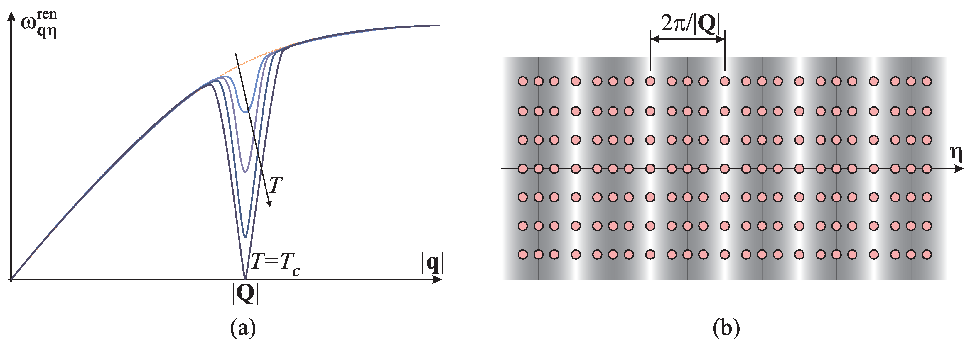
Figure 1. Schematic presentation of the Kohn anomaly: (a) Softening of the phonon mode ω Q η r e n with wave vector q = Q and polarisation η . The arrow depicts a decrease in temperature, ending with the critical temperature T c for which ω Q η r e n = 0 . (b) The crystal lattice in a real space, modulated by the “frozen” phonon of periodicity 2 π / Q along direction η , exhibiting an uniaxial CDW (electron density is depicted by shades of grey).
Symmetry 17 01135 g001
Figure 2. (a) The scattering process in free electron gas, from initial (grey) to final (red) states, by static perturbation of wave vector q . The Fermi sea of the wave number k F is in 1D simply a line between ± k F , in 2D a circle and in 3D a sphere of radius k F . The overlapping region is forbidden as a final state due to the Pauli principle (at zero temperature). (b) The static electron susceptibility Equation (15) of a free electron gas depending on dimensionality of the system, i.e., 1D, 2D and 3D ( q is the wave vector of response, k F is the Fermi wave number), shown schematically in arbitrary units. Full curves are the zero-temperature results, while the dashed ones are the finite temperature corrections.
Symmetry 17 01135 g002
Figure 3. Schematic crystal structure of two examples of quasi-1D systems: (a) organic conductor (TMTSF)2 PF 6 ; (b) transition metal bronze K 0.3 MoO 3 (“blue bronze”). Highly conducting x-direction is along the molecular stacks (vertical in picture); y-direction of reduced conductivity is perpendicular to the stacks (horizontal in picture).
Symmetry 17 01135 g003
Figure 4. Schematic presentation of low-temperature phase diagrams of organic conductors. (a) Phase diagram of Bechgaard and Fabre salts at the domain of pressure (p) and temperature (T). It contains a variety of different phases such as: SP—the spin–Peierls phase (electronic CDW with antiferromagnetic order of their spins); AF—antiferromagnetic phase; SDW—spin density wave phase; SC—superconducting phase; CL—charge localisation phase; M—metallic phase, in which we recognise regimes of 1D, 2D and 3D (Fermi liquid) metallic behaviour. The arrows indicate the ambient pressure phase for the particular material. QCP is the zero-temperature quantum critical point between the SP and AF phases. (b) The ( p , T ) diagram of (TMTSF)2 PF 6 with added dependence on magnetic field B. FISDW denotes the cascade of field-induced SDW phases. Diagrams are redrawn based on data from (a) Ref. [19] and (b) Ref. [72], respectively.
Symmetry 17 01135 g004
Figure 5. The Fermi surface of quasi-1D metal according to Equation (18), consisting of two open sheets (right/left) slightly corrugated around ± k F , in the Brillouin zone spanning between ± π / a x along k x and ± π / a y along k y . Vector Q = ( 2 k F , π / a y ) is the nesting vector. (a) The case of perfect nesting by vector Q for t y = 0 , mapping the left FS sheet exactly to the right one. (b) The case of the imperfect nesting by vector Q for t y 0 , when the left FS sheet is mapped (dashed curve) imperfectly to the right one, leaving electron pockets of finite size on the Fermi surface. (c) The best vector of imperfect nesting Q (vs. Q plotted dashed), in the sense of maximising the susceptibility, is connecting the inflexion points of Fermi sheets.
Symmetry 17 01135 g005
Figure 6. (a) The perfectly nested quasi-1D Fermi surface with vector Q = ( 2 k F , π / a y ) is equivalent to the 1D problem, i.e., dispersionless in the k y -direction, with the 1D nesting vector Q = 2 k F . (b) The equivalent 1D linearised dispersion (19) (full line) derived from the quasi-1D dispersion (16) (dashed curve). D is the energy cut-off introduced due to linearisation, related to the band-width, on the order of the Fermi energy ε F .
Symmetry 17 01135 g006
Figure 7. (a) The gap opening process Equation (22) for linearised dispersions (19) with origins of k chosen at the point of degeneracy lifting. It corresponds to the original dispersion (16) with a gap opened at ± k F . (b) Electron DOS in the ordered state, exhibiting a gap of 2 Δ symmetrically opened around the Fermi energy ε F .
Symmetry 17 01135 g007
Figure 8. Upper panel: Schematic presentation of real space of 1D (or analogously quasi-1D) system, k F = π / 2 a (half-filling of the band): (a) metallic state ( T > T c , Δ = 0 ) with lattice constant a and homogeneous electron density along the chain ρ 0 ( r ) ; (b) the CDW state ( T < T c , Δ 0 ) for the case of Q = 2 k F = π / a for which lattice gets dimerised, with electron density ρ ( r ) modulated accordingly, where r is direction along the chains coinciding with the direction of phonon polarisation η . Lower panel: Experimental observation of the CDW state in TTF-TCNQ in the STM (scanning tunnelling microscopy) imaging. (a) Normal state recorded at T = 63 K, higher than critical temperature T c = 54 K, molecular stacks are in the perpendicular direction (triplet structures are TCNQ, and the doublets in between are TTF molecules). (b) STM picture recorded at T = 49.5 K (left) and its Fourier transform into reciprocal space with obvious dimerisation ( a 2 a ) of the structure (right). Figures in lower panel are obtained by the processing of experimental data shown in figures in Ref. [73].
Symmetry 17 01135 g008
Figure 9. Schematic crystal structure of three examples of quasi-2D materials: (a) high-T c superconducting cuprate YBa 2 Cu 3 O 7 p (“YBCO”); (b) intercalated graphite compound CaC 6 ; (c) transition metal dichalcogenide 2H-NbSe 2 . The conducting ( x , y ) -planes are those along the CuO squares, and graphene or niobium hexagons, respectively (horizontal in picture).
Symmetry 17 01135 g009
Figure 10. (a) Generic phase diagram of high-T c superconducting cuprates at temperature versus hole-doping domain, exhibiting a vast number of different ground states: antiferromagnet (AF), pseudo-gap (PG), charge ordering (CO), superconductor (SC), charge density wave (CDW), strange metal (SM), Fermi liquid (FL). CDW phase here appears as enhanced CO with much longer correlation length under a strong external magnetic field of several dozen Tesla. (b) Phase diagram of NbSe 2 at temperature versus pressure domain containing CDW and SC phases. The zero-temperature quantum phase transition CDW ↔ SC is present at 4.6 GPa. Diagrams are redrawn based on data from: (a) Ref. [34], (b) Refs. [75,76,77], respectively.
Symmetry 17 01135 g010
Figure 11. The ARPES image, i.e., the spectral function intensity imaging the Fermi surface: (a) YBCO for hole doping of 0.11 (left) and 0.28 (right); see phase diagram in Figure 10a; (b) CaC 6 at T = 14 K with Fermi energy ∼ 1.5 eV above the Dirac point (normal state); (c) 2H-TaSe 2 at T = 180 K (normal state). Diagrams are redrawn based on processed data from images in: (a) Ref. [78], (b) Ref. [79], (c) Ref. [80], respectively. Each Brillouin zone is shown in the orange frame, while parts of the Fermi surface in each image are sketched by the yellow curve. In Figure (a), left panel, the full yellow curve is a closed contour based on Fermi liquid theory and d-symmetry of the gap at anti-nodal points, backed by the frequency of oscillations in magnetoconductivity, while the dashed blue is the result of non-Fermi liquid correlated electron theory reproducing the arc-looking high-intensity spectral function around nodal (light blue) and suppressed intensity around the anti-nodal points (dark blue) [81].
Symmetry 17 01135 g011
Figure 12. The Fermi surface topological reconstruction process in which two bands ϵ ± ( k ) appear according to Equation (26). (a) Electrons, with initially closed, circular Fermi surface of radius k F , are scattered on the periodic CDW potential with wave vector Q = ( Q , 0 ) . (b) An open Fermi surface is formed in the new Brillouin zone (dashed rectangle) of the size ( Q / 2 , Q / 2 ) in the k x direction by lifting the degeneracy due to the finite CDW order parameter Δ . (c) In the region of the Fermi surfaces overlap, the emerging bands form the hyperbolic point at energy ε H in the lower, and the elliptic point at energy ε E in the upper band.
Symmetry 17 01135 g012
Figure 13. (a) The process of Fermi surface reconstruction (red curve) as Q is reduced from a value larger than 2 k F to values smaller than it. In the last panel, the Fermi surface in the upper band (blue) is formed. (b) One quarter of the reconstructed Fermi surface (shaded) shown in (a), inside the Brillouin zone spanning ( Q / 2 , Q / 2 ) ( 1 , 1 ) in scaled variables, enclosed by the function κ y F ( κ x ; δ ) κ y ( κ x ; ϵ , δ ) | ϵ = ϵ F (red curve). Quantity κ 0 is an arbitrary scale along κ x chosen under condition δ κ 0 1 . (c) Dependence of scaled Fermi energy ϵ F on ϵ F 0 obtained by solving the Equation (33) before reaching an optimum for ϵ F = ϵ F 0 (marked by red dot), i.e., by putting ϵ F 0 into the LHS. It demonstrates how the Fermi energy of the reconstructed system changes by changing Q (the overlap of Fermi pockets).
Symmetry 17 01135 g013
Figure 14. (a) Numerical results for the zero-temperature order parameter and critical coupling. The quantum transition from the unordered state with zero-order parameter to the CDW state appearing at λ = λ c 0.611 on the electron–phonon coupling strength domain [53]. Order parameter in the vicinity of the critical point λ c is described by Equation (44). (b) The critical value of electron–phonon coupling required for the onset of the CDW, depending on the effective dimensionality d of the metallic system with parabolic electron dispersion, emerging from the theory [54]. Value d = 1 is an effective 1D or perfectly nested system with infinitesimally small critical coupling; see Equation (25). Increasing the effective dimensionality, the critical coupling monotonously increases through the value of 0.611 for d = 2 to 0.8 for d = 3 . (c) DOS of the system with reconstructed Fermi surface (red) forming a logarithmic van Hove singularity at the energy of the hyperbolic point ε H in the lower band and Heaviside step at the energy of the elliptic point ε E at the bottom of the upper band. The 2 Δ -wide interval of depleted DOS, compared to the initial (constant) value g F 2 D (dashed blue), between ε H and ε E , we refer to as the pseudo-gap. Fermi energy ε F is optimally positioned between the two self-consistently created van Hove singularities.
Symmetry 17 01135 g014
Figure 15. Schematic presentation of one 2D layer in the CaC 6 system in a real (a) and reciprocal (b,c) space. The dashed orange rhombus denotes the unit cell of the CDW-reconstructed system (in both spaces). (a) The electron CDW (blue shaded) in the π bonds of the chemically doped graphene with crests along the armchair direction, periodically spreading along the zig-zag direction. Carbon atoms form the honeycomb lattice (unit vectors are a 1 , 2 , a | a 1 , 2 | 2.5 Å; the area of the cell is V C 5.41 Å 2 ). Ca atoms (circles) form the hexagonal superlattice (unit vectors are b 1 , 2 , b | b 1 , 2 | = 3 a 4.32 Å, the area of the cell is V CaC 6 16.16 Å 2 ). The CDW is characterised by the vector W = 3 b 1 that triples the CaC 6 cell along b 1 . The Ca-lattice distortion (displacement of the Ca atoms under the CDW crests by 0.06 ± 0.02 nm) is depicted by the dashed circles. (b) The dashed hexagon represents the carbon Brillouin zone (BZ), with standard Γ , K, K’ points (reciprocal unit vectors are a 1 , 2 * , a * | a 1 , 2 * | 2.9 Å 1 ). The triangles placed at the K, K’ points represent the Fermi surfaces (FS) of the chemically doped carbon layer [79]. The Ca-superlattice (unit vectors are b 1 , 2 * , b * | b 1 , 2 * | 1.68 Å 1 ) folds the carbon BZ, reducing its size to a three times smaller CaC 6 BZ (solid hexagon). The six FS pockets, from the initial carbon K and K’ points, fall into the Γ point. Each is approximated by a circle of the same area S F 0 (dashed red circle). The chemical doping of ξ 0.2 electrons per carbon atom determines the area of the Fermi pocket S F 0 = 2 π 2 ξ / V CaC 6 0.244 Å 2 , giving an average Fermi wave number k F 0.28 Å 1 . (c) The CDW potential, with the wave vector Q b 1 * of periodicity Q = b * / 3 0.56 Å 1 , reduces the CaC 6 BZ, relating the initial FSs in a way to touch or slightly overlap.
Symmetry 17 01135 g015
Figure 16. (a) Schematic presentation of the 2D in-plane vibrations of the Ca-superlattice, placed upon the graphene lattice (light blue) in real space. Circles denote the Ca atoms of mass M in the hexagonal structure, by (n,m) denoting atomic positions at R n m = n b 1 + m b 2 , n, m are integers. Here, b 1 = 1 2 b ( 3 , 1 ) and b 2 = b ( 0 , 1 ) are the unit vectors of the structure in the Cartesian basis ( x ^ , y ^ ) , b is the lattice constant. Vibrations of the Ca atoms are modelled by the first-neighbour harmonic forces, parametrised by the elastic constant K , along three characteristic directions determined by the symmetry. Those are described by unit vectors v 1 = ( 0 , 1 ) , v 2 , 3 = 1 2 ( 3 , 1 ) . Vibrating atom is displaced from the equilibrium position R n m by d n m . (b) Phonon LA and TA in-plane modes ω ( k ) for the 2D hexagonal lattice in units K / M . The phonon dispersion is described depending on the wave vector k , which is taken along the characteristic directions in the Brillouin zone Γ M K Γ (inset). The Ca BZ is spanned by reciprocal vectors b 1 * = 4 π 3 b ( 1 , 0 ) and b 2 * = 2 π 3 b ( 1 , 3 ) in Cartesian reciprocal space ( x ^ * , y ^ * ) . Q is the wave vector of the phonon mode related to the CDW. (c) The chart presenting the values of dimensionless ARPES electron–phonon coupling along directions across the BZ, obtained numerically by ab initio calculations. The picture is reconstructed from the data provided in Ref. [90], where it is compared to experimental data as well.
Symmetry 17 01135 g016
Figure 17. Comparison of experimental results (upper panel, from Ref. [35], Figure 2d, Figure 3a and Figure 6a respectively, under Licence by courtesy of Springer Nature) with the theoretical results (lower panel) [55]. (a) The Fermi surface-driven CDW instability determines the CDW wave vector (its magnitude and direction) of length Q 2 k F 0 = | b 1 * | / 3 directed along the direction of b 1 * of the CaC 6 Brillouin zone that gets shrunken three times along it. In real space, this corresponds to the tripling of the CaC 6 unit cell along the b 1 direction (orange rhombus) defining the CDW wave vector W = 3 b 1 . Charge stripes form the crests (blue shaded) along the b 2 direction. Those appear periodically at distances equal to 4.5 graphene lattice constants a (which is related to the Ca lattice constant as b = 3 a ). In the STM experiment (upper panel), the stripe crest is along the yellow line, while the orange rhombus is the CDW-extended CaC 6 unit cell corresponding to the one in the lower panel. (b) The pseudo-gap of width 2 Δ is opened in the electron DOS g ( E ) (red curve) around the Fermi energy E = ε F , where Δ is the CDW order parameter. The dashed blue line is the electron DOS in the metallic state (in graphene, it is linear in energy). In the experiment (upper panel), the differential conductivity of the STM tunnelling current (proportional to LDOS) vs. the bias voltage with respect to the Fermi energy is measured, and the pseudo-gap of width 2 Δ is observed. (c) Static deformation of the initial Ca lattice (dashed circles and blue hexagon) by the “frozen” TA phonon mode due to the CDW: Ca atomic displacements (red arrows) are along the polarisation direction η T A b 2 . That particular phonon mode displaces the Ca atoms at R n m by d n m η T A cos ( Q · R n m ) by shifting the chains B (CDW crests) by + d and chains A, C by d / 2 along the η T A direction ( d Δ ). The Ca hexagon in the deformed lattice (full circles) is depicted by a yellow contour, corresponding to the experimentally observed STM pattern indicating positions of Ca atoms (yellow hexagon in the upper panel).
Symmetry 17 01135 g017
Figure 18. Irreducible phonon self-energy contributions, phonon propagators are dashed, electron propagators are full lines. (a) Polarisation (“bubble”) diagram as calculated within the standard weak-coupling theory. (b) Cubic anharmonic term. (c,d) Quartic anharmonic terms.
Symmetry 17 01135 g018
Figure 19. Properties of the NbSe 2 TMD based on calculations in Ref. [105]. (a) The (half) Brillouin zone with contours of the Fermi surface. (b) The electron DOS calculated in standard RPA (black curve) and anharmonic MMA (red curve) versus experimental data (dotted curve) from Ref. [104], indicating the pseudo-gap around the Fermi energy E F . (c) The LA phonon mode dispersion along the Γ M line in reciprocal space. The black curve is the high-temperature bare phonon dispersion. Dashed curves in RPA (blue) and MMA (red) are phonon dispersions with electron–phonon interaction taken into account at temperature T = 303.5 K, which is the transition temperature predicted by the RPA (mean-field). The full red curve is the phonon dispersion in MMA at the CDW transition temperature T MMA = 33.5 K, yielding the CDW wave vector in accordance with experimental observations. In the MMA calculations, only the self-energy corrections were kept (Figure 18c), while the vertex corrections (Figure 18b,d) were neglected by virtue of the Migdal theorem due to large momentum transfer by Q CDW . All figures are reconstructed based on data from Ref. [105].
Symmetry 17 01135 g019
Disclaimer/Publisher’s Note: The statements, opinions and data contained in all publications are solely those of the individual author(s) and contributor(s) and not of MDPI and/or the editor(s). MDPI and/or the editor(s) disclaim responsibility for any injury to people or property resulting from any ideas, methods, instructions or products referred to in the content.