Abstract
Circular polarization detection plays a significant role in various fields, such as optical communication, quantum information processing, biomedical detection, polarization imaging, and sensing. Traditionally, similar to linear polarization detection, circular polarization detection is realized by systems composed of discrete optical components, which tend to be bulky and complex. With the advancement of technology, there is a growing demand for efficient and compact integrated circular polarization detectors. In this review, we focus on two advanced research areas concerning integrated circular polarization detectors: those based on asymmetric materials or structures. We explore recent advances and future prospects and challenges for the development of integrated circular polarization detectors.
1. Introduction
Circularly polarized light (CPL) is characterized by the electric field rotating with a constant magnitude in a plane perpendicular to the direction of propagation. The expression for CPL propagating along the z-axis can be written as , where is the electric field amplitude, ω is the angular frequency, φ is the phase difference, and are the unit vectors along the x- and y-axes, respectively. When φ = −π/2, the wave corresponds to left-handed circularly polarized (LCP) light, while φ = +π/2 corresponds to right-handed circularly polarized (RCP) light. These two circular polarization states correspond to the two spin states of photons. Due to its unique interaction with chiral materials [], its resilience to scattering [,], and the quantum information carried by photon spin states [,], CPL has vast potential for applications in optical communication [,], quantum information processing [,,], biomedical diagnostics [,,], as well as polarization-based imaging and sensing [,,,]. Traditionally, circular polarization detection, like linear polarization detection, has been achieved through systems composed of discrete optical components. However, these systems tend to be bulky and complex, making them less suited for miniaturized applications. The circular polarization extinction ratio (CPER) represents the ability of a detector to distinguish between circularly polarized light of opposite handedness. CPER is an important metric for comparing the performance of various circular polarization detectors. Specifically, it quantifies the ratio of the response or transmittance of the detectors to circularly polarized light of a specific handedness relative to the opposite-handedness circular polarization. To promote the advancement of circular polarization detection technologies, developing integrated circular polarization detectors with small size, high responsivity, and high CPER has become a core challenge.
Asymmetric materials provide a direct approach to circular polarization detection. Compared with traditional detectors, circular polarization detectors based on asymmetric materials offer a more compact device structure, as they do not require additional processing steps []. In recent years, chiral perovskite and organic materials [,,], along with asymmetric two-dimensional [,] and topological materials [,], have been shown to effectively resolve circularly polarized light. However, the limited selection of asymmetric materials for circular polarization detection has resulted in a narrow range of detectable wavelengths. Moreover, challenges such as poor chemical stability, low responsivity, and low CPER have hindered the further development of integrated circular polarization detectors based on asymmetric materials.
With the advancement of micro–nanofabrication techniques, integrated circular polarization detectors based on asymmetric structures have been developed to enhance detector performance [,,,]. In recent years, the inherent chirality of symmetry-broken structures has been discovered through the in-depth study of topological optics and bound states in the continuum [,,]. This discovery indicates that such structures can exhibit different absorption or transmission characteristics for LCP and RCP light. This property significantly enhances the CPER of the materials, making them more sensitive and effective in circular polarization detection [,]. Furthermore, Chiral metamaterials, which allow for the arbitrary customization of geometric shapes, sizes, and material compositions, exhibit strong chiral characteristics and light manipulation capabilities [,,,]. By integrating these metamaterials with various detection materials, efficient circular polarization discrimination and improved optical coupling efficiency can be achieved for specific target wavelengths [,,].
In this review, Section 1 concentrates on integrated circular polarization detectors that are based on asymmetric materials. Section 2 then proceeds to discuss integrated circular polarization detectors based on asymmetric structures. Finally, in Section 3, we explore the challenges and opportunities for integrated full-Stokes polarization detectors.
2. Integrated Circular Polarization Detectors Based on Asymmetric Materials
Since most materials are not sensitive to polarization, traditional methods for circular polarization detection typically rely on mechanically rotating polarizers and waveplates. However, this approach requires the use of numerous optical components and the construction of complex, precise detection setups, which hinders the miniaturization and integration of circular polarization detection systems. As a result, researchers have extensively explored the use of asymmetric materials to develop more compact and integrated circular polarization detectors.
2.1. Chiral Perovskite and Organic Materials
Chiral materials are defined as objects that cannot be superimposed on their mirror images. Chiral perovskites and organic materials are compounds with strong circular dichroism (CD), enabling direct detection of circularly polarized light without the need for any additional optical components. This characteristic makes them promising candidates for the development of miniaturized and integrated circular polarization detection systems. Furthermore, these materials can be prepared using solution-processing techniques, which offer lower cost and higher fabrication flexibility. With excellent mechanical flexibility, they are well-suited for developing circular polarization detectors in flexible electronic devices, thus broadening their range of potential applications.
In 2019, Chao Chen et al. fabricated a direct CPL detector using chiral organic–inorganic hybrid (α-PEA) PbI3 perovskites as shown in Figure 1a. The chiral organic–inorganic hybrid combines the polarization-sensitive absorption properties of chiral organic materials with the efficient charge transfer characteristics of inorganic materials, enabling the device to achieve a responsivity of 795 mA W−1 and a detectivity of 7.1 × 10¹¹ Jones []. The detector exhibits a maximum CPER of approximately 1.1 at 395 nm, but it cannot achieve high-resolution circular polarization detection.
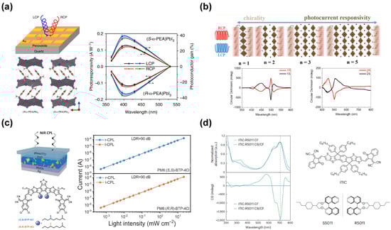
Figure 1.
(a) Schematic diagram of a circular polarization detector and the structure of chiral perovskite. The responsivity and photoconductor gain of (R- and S-α-PEA) PbI3 device under LCP and RCP light at the wavelengths of 365, 395, 430, and 530 nm []. (b) Schematic diagram of quasi-two-dimensional chiral perovskite thin films. Circular dichroism (CD) spectra of the device with inorganic layers of 1 and 2 layers, respectively []. (c) Device configuration for the near-infrared circular polarization detector and molecular structure of the detection material. Light-intensity-dependent photocurrent under 830 nm circularly polarized illumination []. (d) Molecular structures of ITIC and R/S5011. Thin-film absorption and CD spectra chiral and nonchiral ITIC blend films [].
In 2022, Tianjun Liu et al. investigated quasi-2D perovskite (NEA)2(MA)n-1PbnI3n+1 films for CPL detection in devices, as illustrated in Figure 1b, addressing the trade-off between the ability to differentially absorb circularly polarized light and the photocurrent responsivity in chiral perovskite devices []. The device achieved a maximum CPER of 1.16 and a responsivity of 15.7 A W−1.
In 2022, Lixuan Liu et al. developed direct CPL detectors based on bulk heterojunctions (BHJs) composed of the chiral BTP-4Cl nonfullerene acceptor and dilute achiral PM6 donor [], as shown in Figure 1c. The supramolecular chirality of the acceptor aggregates imparts a true absorption CPER of 1.02 at 830 nm to the BHJs, the highest among near-infrared sensitive detectors. This results in a photocurrent CPER of 1.03 for the photodetector. The device demonstrates an external quantum efficiency of 60%, a responsivity of 0.4 A W−1, and a detectivity of 3 × 10¹¹ Jones.
In 2023, Li Wan et al. introduced a strategy to induce strong CD in planar nonfullerene acceptors, achieving near-infrared (NIR) CPL detection [], as depicted in Figure 1d. Utilizing chiral ITIC blends, they demonstrated proof-of-concept circularly polarized organic photodiodes with a dissymmetry factor exceeding 0.1. These devices are able to cover the 650–1000 nm range for CPL sensing. Under 700 nm illumination, the photodetector exhibited a responsivity of 0.4 A W−1 and a detectivity of 1.04 × 10¹³ Jones. Photocurrents under left-handed and right-handed CPL illumination were 0.55 mA and 0.60 mA, respectively, resulting in a CPER of 1.09.
2.2. Asymmetric Two-Dimensional Materials and Topology Materials
Chiral perovskite and organic materials have been demonstrated to possess the capability for direct detection of circular polarization. However, these materials are confronted with significant challenges, including their poor chemical stability and inadequate CPER. Moreover, the restricted availability of materials confines their functionality to the visible to near-infrared spectrum. The emergence of inorganic materials, notably two-dimensional inorganic materials, presents a promising solution to these issues. In recent years, two-dimensional materials have garnered widespread attention in optoelectronics due to their unique optical and electronic properties. In particular, asymmetric two-dimensional materials, with their anisotropic optical characteristics, offer promising potential for the development of CPL detectors based on these materials. Meanwhile, topological materials, with their distinctive electronic band structures, introduce novel optoelectronic phenomena such as the Berry curvature effect of electronic wavefunctions []. The circular photogalvanic effect (CPGE) is a distinctive photocurrent phenomenon that occurs when CPL illuminates a material. The interaction of the spin angular momentum carried by photons with the electronic band structure gives rise to an asymmetric carrier excitation in systems where inversion or time-reversal symmetry is broken. This asymmetry gives rise to a directional photocurrent, even in the absence of an external electric field. The combination of the unique optical properties of asymmetric two-dimensional materials with the innovative physical characteristics of topological materials opens up new avenues for the development of integrated circular polarization detectors. These detectors not only have the ability to efficiently detect and discriminate between circularly polarized light with different handedness, but they also hold the potential for integrating additional functionalities, thereby enhancing device performance and expanding their range of applications.
In 2018, Su-Yang Xu et al. observed the Berry curvature dipoles induced by nontrivial wavefunctions in monolayer WTe2 using mid-infrared photoelectronic microscopy [], as depicted in Figure 2a. They revealed the phenomenon of the circular photogalvanic effect (CPGE), which can be controlled by an external electric field. The phenomenon known as the CPGE is attributed to the distinctive inverted band structure and tilted crystal lattice of the material. In this case, the direction of the induced photocurrent undergoes a reversal upon alteration of the handedness of the light. In the unipolar photoresponse region, the device achieves a maximum CPER of 3.56. Moreover, the observed CPGE remains consistent over a wide range of charge densities and exhibits strong displacement field modulation, highlighting its significant potential for applications in integrated circular polarization detectors.
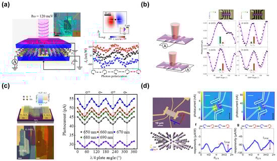
Figure 2.
(a) Schematic experimental setup for detecting the mid-infrared circular photogalvanic effect (CPGE) on a dual-gated monolayer WTe2 device. Photocurrent along the a-axis varying with polarization state []. (b) Diagram of the device indicating the axis along which the current is probed. SEM image of the measured device and crystal orientation, showing data (black dots) for photocurrent measured along the longitudinal/transverse axis of the Hall bar []. (c) Schematic diagram of the SL-MoS2/FL-MoS2 homojunction device along with its optical microscope and fluorescence image. The photocurrent as a function of the λ/4 plate angle at zero bias with various excitation wavelengths []. (d) The optical microscopy of a Hall-shaped Te device and the lattice structure of Te. Scanning photocurrent images of the Te device under 10.6 μm and 4.0 μm excitation, respectively, along with θλ/4-dependent photocurrent responsivity under the same excitations [].
In 2019, Gavin B. Osterhoudt et al. demonstrated a large bulk photovoltaic effect (BPVE) in microscopic devices of the Weyl semimetal TaAs in the 10.6 µm band at room temperature [], as shown in Figure 2b. By measuring the photocurrent response of TaAs devices along different axes under varying polarization conditions, they were able to distinguish between contributions from displacement current and photothermal effect (PTE). The fourth-harmonic sine term (LS) was nearly five times larger than the cosine term (LC), indicating that the dominant response was due to displacement current (sin(4Φ)—LS). In contrast, in devices lacking in-plane broken symmetry axes (ab-plane devices), only the cosine term related to thermal response (cos(4Φ)—Lc) was observed. The device achieved a CPER of 1.72. The investigation of the nonlinear optical properties of TaAs revealed a correlation between the CPGE and the electronic chirality of TaAs.
In 2021, Chen Fang et al. demonstrated a self-powered, filterless on-chip full-Stokes polarimeter based on a 45-degree tilted single-layer MoS2/few-layer MoS2 homojunction [], as illustrated in Figure 2c. Since most single-layer (SL) transition metal dichalcogenides (TMDCs) are in-plane isotropic, they typically exhibit a distinct CPGE response only under oblique incident excitation. Under a light excitation with a power density of 60 μW cm−2, the zero-bias homojunction device showed a significant helicity-dependent photocurrent across the 650–690 nm wavelength range with a CPER of approximately 1.1. However, the CPGE in the SL-MoS2 device was too weak to be detected under the same excitation conditions.
In 2022, Junchao Ma et al. precisely controlled and measured the photoresponse of Te under circularly polarized light at different wavelengths [], as shown in Figure 2d. They observed a reversal in the sign of the CPGE response at wavelengths of 10.6 μm and 4.0 μm, providing direct evidence of Weyl-related optical responses in tellurium. These two distinct wavelengths correspond to critical transitions between the bands of different Weyl cones, and the sign of the CPGE is determined by the chirality selection rules within a specific Weyl cone and between two different Weyl cones. The device achieved a CPER of 1.47 and 1.80 at 10.6 μm and 4.0 μm, respectively.
3. Integrated Circular Polarization Detectors Based on Asymmetric Structures
In the previous section, circular polarization detection is achieved through the utilization of asymmetric materials, such as chiral perovskites and organic materials, two-dimensional materials, and topological materials. However, the selection of such asymmetric materials remains constrained, resulting in a limited wavelength range suitable for practical applications. Moreover, integrated circular polarization detectors based on asymmetric materials encounter several challenges, including a reduced CPER, difficulty in tuning the response spectrum, and the complexity of large-scale integration. With advancements in micro- and nanofabrication technologies, the development of integrated circular polarization detectors based on asymmetric structures has gained significant attention [,]. The fabrication of artificial micro- and nanostructures with circular polarization discrimination capabilities has become a key research focus, offering new opportunities for high-performance detection.
3.1. Inherent Chirality of Symmetry-Broken Structures
Recently, chiral bound states in the continuum (BICs) have been proposed to enable maximum chirality over a subwavelength thickness. Similar to the natural chirality of the material, chiral BIC structures achieve inherent chirality by simultaneously breaking both in-plane and out-of-plane mirror symmetry [,,]. Additionally, bilayer Moiré metasurfaces realize intrinsic chirality by breaking interlayer symmetry, resulting in chiral anisotropy for both positive and negative k directions.
In 2022, Tan Shi et al. realized a planar chiral metasurface with in-plane arrays of symmetry-reduced meta-atoms [], as shown in Figure 3a. This metasurface, controlled by the physics of BICs with strong birefringence in a continuous medium, is identified as a vortex-polarization singularity surrounded by elliptical characteristic states with nonzero helicity. By illuminating with symmetry breaking, the BIC state can be transferred to a strongly external chiral q-BIC with tunable linewidth and polarity. Through the introduction of in-plane structural asymmetry, the metasurface achieves a maximum CPER of 199 (theoretical) and 27.6 (experimental) under normal incidence.
In 2023, Yang Chen et al. proposed the optical realization of intrinsic chiral BICs based on slant-perturbation metasurfaces []. As illustrated in Figure 3b, the metasurface is composed of a square array of slanted trapezoidal nanoholes in a TiO2 film, placed on a glass substrate, and covered with PMMA. This structure is evolved from vertical square nanoholes by introducing two types of perturbations: an in-plane deformation angle α and an out-of-plane slant angle φ, both of which break all mirror symmetries. Experimentally, a quality factor (Q-factor) as high as 2663 and a CPER value of 13.4 were observed.
In 2023, Bokun Lyu et al. revealed the origin of chirality in the Moiré metasurface under normal incidence using the chiral coupled oscillator model [], as shown in Figure 3c. Based on the properties of the non-Hermitian Hamiltonian, the chirality can be enhanced by breaking the layer-to-layer symmetry, which enables chiral anisotropy in both forward and backward directions. These findings were verified through a proof-of-concept experiment. The maximum CPER obtained from simulations was 65.7, while the value measured in preliminary experiments was 9.5. This work endows twistronics and Moiré physics with additional degrees of freedom by tailoring the symmetry of the system, which can control the properties of light fields, such as polarization, phase, spatial distribution, and asymmetric transmission.
In 2024, Xinbo Sha et al. demonstrated hybrid resonant metasurfaces by combining the concepts of chiral quasi-BICs and phase-change materials [], as illustrated in Figure 3d. By exploiting the inverse dependence of the out-of-plane offset on asymmetry, two resonances with maximum opposite chirality were achieved at the Γ-point of the spectrum. The phase transition between the amorphous and crystalline phases allows for precise control of the chiral response. The maximum CPER reaches 46.6.
In 2024, Weijin Chen et al. uncovered the origin of the strong chiral responses in resonant nanostructures [], as depicted in Figure 3e. They revealed that the reactive helicity density plays a significant role in generating chiral radiation, which can be dominant over the optical chirality density. They proposed a general method for achieving maximum chirality in planar nanostructures, demonstrated through a bilayer planar photonic crystal slab and a bilayer metasurface. In this approach, in-plane symmetry is broken by the shape of the nanostructures themselves, while out-of-plane mirror symmetry is broken through the bilayer design. The simulation results of the bilayer metasurface structure yield a CPER of 65.7. Moreover, Chunhua Qin et al. introduced a novel approach to achieve chiral quasi-BICs by strategically manipulating the structural symmetry through the rotation of one of the paired plasmonic bricks []. By fine-tuning the rotation angle, the radiation loss in the quasi-BICs can be precisely modulated, enabling a critical transition from a half-wave plate to an efficient absorber for LCP light. The rotation-induced chiral quasi-BICs achieve a CPER of approximately 2.1 at 920 nm.
In 2024, Jiaxin Zhou et al. leveraged the high refractive index induced by excitonic resonance and symmetry-broken nanostructures in layered tungsten disulfide (WS2), as shown in Figure 3f, to generate quasi-bound states in the continuum within the WS2 metasurface. This enabled complete phase regulation of 2π in an ultrathin structure with a thickness of only 35 nm. Furthermore, they experimentally demonstrated holographic display for different circularly polarized incident light by utilizing the resonance of excitonic van der Waals metasurfaces [].
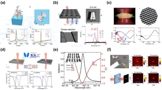
Figure 3.
(a) Schematic of the symmetry-breaking processes that transfer the BIC to planar chiral q-BICs. Simulated transmission Jones matrix spectra and circular dichroism (CD) spectra of the metasurface under two conditions: with a symmetric structure parameter at oblique incidence and with an asymmetric structure parameter at normal incidence []. (b) Schematic of the slant-perturbation metasurface to realize intrinsic chiral BICs. Measured reflection spectra of the two metasurface samples of 68 μm and 200 μm sizes under LCP and RCP incidence, respectively []. (c) Schematic illustration of the twisted Moiré metasurface. The measured results of transmission spectrum and CD spectrum []. (d) Schematic picture of hybrid phase-change metasurface. The LCP and RCP transmission spectra in the amorphous and crystalline phase []. (e) Schematic of the bilayer metasurface for achieving maximum chirality. Reflection spectra of the chiral bilayer metasurface under RCP and LCP incidence, and the corresponding CD spectrum []. (f) Schematic of excitonic WS2 metasurfaces for resonant wavefront shaping, enabling resonantly holographic display using excitonic van der Waals metasurfaces [].
3.2. Chiral Metamaterials for Circular Polarization Selective Discrimination
Inherent chirality based on asymmetric structures can achieve tunable Q-factors and circular polarization discrimination capabilities. However, such structures function similarly to filters in circular polarization detection, achieving polarization discrimination by controlling the transmission or reflection differences in circularly polarized light, which increases the complexity of the device. Chiral metamaterials are a class of artificial composite materials or structures that exhibit chirality at the structural level. In optics, chiral metamaterials can distinguish between LCP light and RCP light, responding differently to each type [,,,,,,,,]. A notable feature of chiral metamaterials is that, compared with natural materials, they are typically composed of unit structures with complex geometries. Through the ingenious design of these chiral structures, it is possible to enhance or suppress the transmission of specific polarization states and selectively couple light of different polarizations. Integrating chiral metamaterials with traditional detection materials not only allows for arbitrary pairing tailored to various detection bands but also simultaneously achieves selective discrimination of circular polarization and improved coupling efficiency, leading to efficient, compact integrated circular polarization detectors.
In 2009, Justyna K. Gansel et al. fabricated three-dimensional gold helical chiral metamaterials using an approach based on direct laser writing into a positive-tone photoresist, followed by electrochemical deposition of gold []. For light propagation along the helix axis, as shown in Figure 4a, the structure blocks circular polarization with the same handedness as the helices, while transmitting the opposite polarization. This structure was used as a compact broadband circular polarizer in the range of 3.5–7.5 μm, with a maximum transmission CPER of 9.3. In 2015, Marco Esposito et al. developed three-dimensional triple-helical nanowires, engineered by the innovative tomographic rotatory growth method, on the basis of focused ion beam-induced deposition []. These three-dimensional nanostructures showed up to 37% circular dichroism in a broad range (500–1000 nm), with a high signal-to-noise ratio (up to 24 dB).
In 2012, Y. Zhao et al. introduced and applied the concept of twisted metamaterials to achieve strong, broadband bianisotropic effects in metamaterials [], as illustrated in Figure 4b. This design is based on stacked planar metasurfaces created using conventional lithographic techniques, with each layer rotated relative to the next. By introducing a twist in the lattice orientation of the metamaterial inclusions, they relaxed the usual fabrication constraints and achieved exotic effects analogous to those of 3D metamaterials, but with much simpler fabrication processes. The more layers are stacked in the twisted metamaterial slabs, the more pronounced the circular dichroism in the transmitted light spectrum becomes. In 2016, Zuojia Wang et al. presented a general method for designing circular dichroism metamirrors within the framework of Jones calculus []. It was analytically shown that the building block of such a metamirror must simultaneously break n-fold rotational symmetry (n > 2) and mirror symmetry. The device achieves a simulated CPER of 18.7.
In 2020, Zhancheng Li et al. proposed a chiral mirror to achieve spin-selective full-dimensional manipulation of optical waves []. For a specific chiral mirror with near-perfect extinction of one circular-polarized illumination, the reflection difference between incident waves with opposite circular polarization states exceeds 78%, as illustrated in Figure 4c. The device achieves a CPER of 4.5. By simply altering three structural variables of the chiral mirror, the proposed design principle enables arbitrary and independent control over the spin-selective manipulation of amplitude, phase, and operation wavelength of circular-polarized waves with a large modulation depth.
In 2020, Lei Kang et al. demonstrated all-optical picosecond light polarization switching using an ultrathin nonlinear chiral metamirror consisting of a 2D array of α-Si split-ring resonators on top of a silver backplane, with a thin silica spacer layer in between [], as depicted in Figure 4d. The proposed metamirror combines the advantages of both dielectric and plasmonic planar optical systems. The linear optical properties of the metamirror—such as sharp chiral-selective absorption and the preservation of circular polarization upon reflection—are primarily attributed to two factors: the extremely low loss of α-Si at optical communication wavelengths and the Fabry-Perot interference enabled by the highly reflective plasmonic backplane. At 1530 nm, the measured CPER is 2.3.
The previously discussed chiral metamaterials rely on transmission or reflection principles, functioning similarly to optical filters within the detector. While they enable circular polarization discrimination, they also reduce the optical flux reaching the active material, leading to low responsivity. Therefore, enhancing the intrinsic detection capability of the photodetector itself is crucial. Shonak Bansal et al. integrated a dual heterojunction structure consisting of p+-bilayer graphene (BLG)/ZnO nanowires/p−-Si and p+-BLG/n−-mercury cadmium telluride (MCT)/n+-MCT, achieving a significant enhancement in detector response across the visible-to-near-infrared and long-wave infrared ranges, respectively [,]. The performance improvement originates from the strong electric field at the heterojunction interface, which effectively accelerates photocarrier generation, leading to a spontaneous photocurrent without the need for an external bias. Moreover, bilayer graphene, nanowires, and MCT benefit from well-established fabrication processes, making them suitable for large-scale production. Photodetectors based on heterojunctions can compensate for the reduced light flux caused by the metamaterial, allowing the device to achieve both high circular polarization discrimination and considerable sensitivity, thus offering a promising pathway toward high-performance circular polarization detection.
In 2023, Yonghao Bu et al. proposed a circular polarization detector that combines two ordinary circular polarization detectors, each with enantiomerically opposite ellipticity dependences and opposite photoresponse polarities []. As shown in Figure 4e, the superposition of the two photoresponses results in an optoelectronic silent state, characterized by a complete absence of photocurrent and a significant reduction in noise. Moreover, the establishment of this silent state can be precisely tuned for various polarization states by carefully modulating the magnitudes of the two photoresponses during superposition. An ultra-high CPER of 1.5 × 10⁵ is realized within the λ (1.36–1.7 μm)-f (1–10 kHz) region when the silent state coincides with a circular polarization state or a chirality transition point (e.g., horizontal or vertical polarization).
In 2024, Zeyang Liu et al. introduced a high-fidelity multichannel metasurface hologram capable of simultaneously multiplexing polarization states and incident angles, as depicted in Figure 4f. Integrated onto a planar glass waveguide, the proposed metasurface hologram consists of silicon (Si) nanopillars with spatially varying orientation angles. By employing geometric phase modulation, the central periodic spatial frequency distribution pattern is encoded onto the metasurface hologram. The spin state of the incident circularly polarized light and the in-plane orientation angle determine the geometric phase, while the orientation angle of the Si nanopillars controls the phase shift modulation. Experimentally, they demonstrated six-channel holographic projection by illuminating the metasurface hologram with incident light of different azimuthal angles and circular polarization states (LCP or RCP) [].
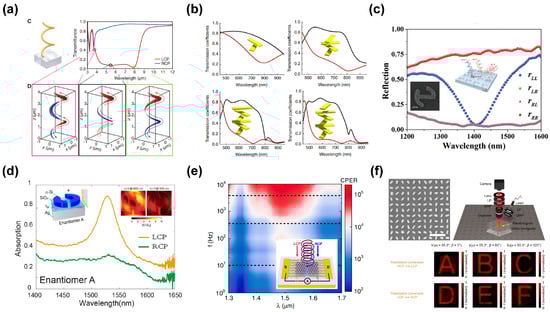
Figure 4.
(a) Schematic diagram of the three-dimensional metallic helical structure and its circular polarization transmission spectra. Snapshots of the electric current distribution along the metal wire for the three wavelengths []. (b) Transmission efficiency of a twisted metamaterial slab with a different number of layers under LCP and RCP illumination []. (c) Schematic diagram of the chiral mirror structure and its experimentally measured reflection coefficients []. (d) The corresponding handedness-dependent total absorption spectra of dielectric-plasmonic hybrid chiral metamirrors. The illustration shows a schematic diagram of a circular polarization detector based on split-ring resonators and the electric field distribution under circularly polarized light illumination []. (e) The device structure of an integrated circular polarization detector dimer based on the metal-MoS2-metal architecture, along with the contour plot of CPER (λ, f) for the detector dimer in the LCP-responsive ultrahigh-CPER mode, as determined by experimental data []. (f) Experimental results of the six-channel metahologram [].
Figure 5 provides an overview of recent advancements in circular polarization detectors based on chiral metamaterials. Based on their detection mechanisms, these detectors can be classified into far-field coupled and near-field coupled photodetectors. In near-field coupled photodetectors, the circular polarization coupling structures are directly integrated with the detection material, resulting in a higher level of integration. In contrast, far-field coupled devices have a separation between the circular polarization discriminating metamaterial or metasurface and the detector, introducing a propagation distance. Near-field coupled detectors leverage the near-field enhancement of photonic modes to improve the absorption efficiency of the detection material, whereas in far-field coupled devices, the presence of the metamaterial or metasurface can partially reduce the optical flux. However, due to diffraction, scattering, and near-field absorption, near-field coupled detectors typically exhibit a lower CPER compared with far-field coupled devices, as shown in Figure 5. In recent years, the emergence of novel near-field coupled circular polarization detectors based on photonic-electronic cooperative manipulation has overcome this limitation. By configuring the photoelectric silent state to the polarization state orthogonal to the primary detection polarization state, the detector achieves a CPER approaching infinity [].
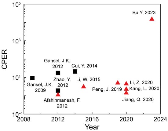
Figure 5.
Research progress of circular polarization detectors. The black squares represent far-field coupled photodetectors [,,,], while the red triangles indicate near-field coupled photodetectors [,,,,,,].
Circular polarization detectors have demonstrated their significance in various real-world applications. For instance, circular polarization imaging technology enables the differentiation between tumors and normal tissues, allowing for noncontact cancer diagnosis [,]. Additionally, polarization image restoration in turbid media based on circularly polarized light has been widely applied []. Furthermore, the polarization-preserving property of circularly polarized light enables high-fidelity free-space optical communication in atmospheric turbulence channels []. At the same time, advancements in circular polarization detection technology have facilitated practical applications in photonic quantum information processing, including photonic computing and cryptography []. The broad applicability of circular polarization detectors, spanning medical diagnostics, polarization imaging, communication technology, and quantum information processing, highlights their diverse potential and technological value. To achieve even higher performance, novel integrated circular polarization detection principles and devices must be introduced. Integrated circular polarization detectors based on asymmetric materials and asymmetric structures have brought new momentum to this field. In this review, we evaluate the performance of integrated circular polarization detectors using key metrics such as CPER, responsivity, response wavelength range, or peak response wavelength. For a circular polarization detector sensitive to LCP light, the CPER is defined as the ratio of the responsivity under LCP and RCP illumination, given by CPER = RLCP/RRCP, where RLCP and RRCP are the responsivities measured under LCP and RCP illumination, respectively. For a detector sensitive to RCP light, the CPER is defined as CPER = RRCP/RLCP. Table 1 summarizes the key performance parameters, including device structures, CPER, responsivity, and peak response wavelength, for some representative circular polarization detectors.

Table 1.
The main performance indicators of various circular polarization detectors.
Organic materials and perovskites can be fabricated through simple solution-processing methods and support large-scale production via roll-to-roll printing technology, which is highly advantageous for reducing manufacturing costs and scaling up production. Additionally, the flexibility of these materials makes them ideal for the fabrication of flexible electronic devices. However, their limited spectral sensitivity range, chemical instability, and poor large-area uniformity restrict their operation to the ultraviolet to near-infrared range. Further optimization of the processing techniques is still required to meet the consistency, repeatability, and reliability standards needed for commercial products. Asymmetric two-dimensional materials and topological materials, due to their tunable band gaps, can cover working wavelengths from the visible to terahertz regions, and their ability to be grown on Si substrates makes them compatible with current electronic device manufacturing processes. However, the degree of asymmetry in these materials is not sufficiently high, leading to a limited ability to distinguish circular polarization. Moreover, achieving high-quality, large-area thin films of most 2D materials remains a challenge.
Circular polarization detectors based on asymmetric structures typically exhibit higher CPER compared with those based on asymmetric materials, as shown in Table 1. However, such structures act like filters and thus reduce the light flux reaching the detector. Additionally, the high performance of these devices depends on precise structural perturbations, placing higher demands on the fabrication process. By combining chiral metamaterials with traditional detection materials, it is possible to achieve selective circular polarization discrimination across any wavelength range, while also improving coupling efficiency to realize high-performance, compact integrated circular polarization detectors. Circular polarization detectors based on chiral metamaterials offer manufacturability and reproducibility for large-scale production, making them suitable for industrial applications and a key research direction for the future. However, the structural design of chiral metamaterials is typically complex, and their subwavelength feature sizes require high-precision fabrication techniques such as electron beam lithography (EBL) or deep ultraviolet (DUV) lithography, making large-scale production costly. Additionally, challenges such as the alignment between metamaterials and conventional detector pixels, as well as crosstalk between adjacent pixels, remain critical issues that need to be addressed.
4. Challenge and Opportunity: Integrated Full-Stokes Polarization Detectors and Artificial Intelligence Algorithms
Integrated polarization detectors have garnered significant attention and research interest over the past few decades. The study of detectors for measuring linear polarization states has been extensive. Recently, there has also been considerable progress in the development of integrated circular polarization detectors. However, single linear polarization detectors or circular polarization detectors still face limitations in fully characterizing polarization information, which restricts their applicability in complex scenarios requiring comprehensive polarization data. By integrating linear polarization detectors with circular polarization detectors, it is possible to create an integrated full-Stokes polarization detector. Such a detector can sense and measure complete polarization parameters (i.e., intensity and the three Stokes parameters), marking the next frontier in polarization detection technology [,,,]. By capturing all polarization states simultaneously, such a device can offer far more comprehensive information about the incident light, enabling a wide range of advanced applications in optical communication, quantum information, biomedical imaging, and remote sensing [,,]. Furthermore, the emergence of artificial intelligence algorithms and other emerging technologies has injected new vitality into the development of polarization detectors. By leveraging artificial intelligence algorithms, polarization detectors can achieve enhanced data processing speed, optimized performance, and improved detection accuracy. However, the development of these integrated full-Stokes detectors and artificial intelligence algorithms presents both significant challenges and exciting opportunities.
In 2021, Yingjie Zhao et al. demonstrated a Stokes-parameter photodetector operating in the visible light range, as depicted in Figure 6a, based on single-crystalline nanowire arrays of chiral 2D perovskites []. The chiral ammonium cations intercalated between the perovskite layers exhibit a strong response to circularly polarized light, with a CPER of 1.2. Meanwhile, the highly aligned nanowires with anisotropic dielectric functions lead to a linear polarization extinction ratio (LPER) of 1.6. Additionally, due to the precise alignment, single crystallinity, and well-defined crystallographic orientation of the nanowires, the device achieves a responsivity of 47.1 A W−1 and a specific detectivity of 1.24 × 10¹³ Jones.
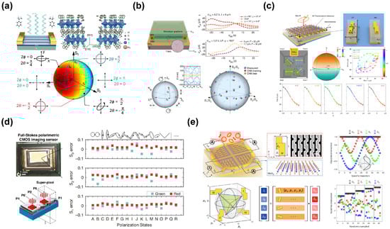
Figure 6.
(a) Crystal structure and device architecture of a Stokes-parameter photodetector. Poincaré-sphere representation for the polarization states of light with various Stokes parameters. The theoretical absorption intensity of 2D chiral perovskite nanowire arrays is depicted by different colors on the surface of the Poincaré-sphere []. (b) Schematic of the TDBG photodetector. The photovoltage of the device has a mapping relationship with polarization states and wavelengths. A CNN is utilized to analyze the full Stokes parameters and wavelengths []. (c) Schematic of the three-ports mid-IR photodetector based on resonance photothermoelectric response. Ports 1 and 2 are used for extracting the azimuth angle θ, while Port 3 is used for extracting the ellipticity angle φ []. (d) Image of full Stokes polarimetric CMOS imaging sensor and the 3D Conceptual illustration of chip integrated full Stokes CMOS polarimetric imaging sensor. Error distribution for Red/Green color full Stokes parameter detection measurement result []. (e) Schematic of the on-chip full-Stokes polarimeter. Geometric representation and matrix representation of the OCM by the four OPEVs. Input and high-accuracy reconstructed polarization states in a specific trajectory on the Poincaré sphere and at different levels of light power [].
In 2022, Chao Ma et al. demonstrated an intelligent full-Stokes polarization photodetector based on twisted double bilayer graphene (TDBG) []. The tunable infrared bulk photovoltaic effect (BPVE) in TDBG arises from Moiré-induced strong symmetry breaking and quantum geometric contribution. As shown in Figure 6b, This BPVE enables the generation of unique photocurrent responses for different polarization states and infrared wavelengths. By employing a trained convolutional neural network, the device achieves accurate prediction of the polarization, power, and wavelength of incident light.
In 2022, Mingjin Dai et al. proposed a three-port polarimeter based on on-chip chiral plasmonic metamaterial-mediated mid-infrared photodetectors for full-Stokes detection [], as illustrated in Figure 6c. Utilizing the polarization-dependent photothermal effect in plasmonic metamaterials and the Seebeck effect in 2D thermoelectric materials, they demonstrated room-temperature, mid-IR polarization-sensitive photodetectors for both linear and circular polarization. The chiral plasmonic metamaterials create localized temperature gradients, generating a polarization-resolved photovoltage response in the thermoelectric material. The LPER of the device can vary from 2 to +∞ and −∞ to −1. The average measurement errors for Stokes parameters S1, S2, and S3 are 14.2%, 15.2%, and 5.4%, respectively.
In 2023, Jiawei Zuo et al. demonstrated a chip-integrated, single-shot metasurface-based full-Stokes CMOS polarimetric imaging sensor (MetaPolarIm) []. As depicted in Figure 6d, the MetaPolarIm consists of subwavelength-thick broadband linear polarization and circular polarization filters, based on double-layer metallic gratings and hybrid chiral metasurfaces, respectively. The device achieves maximum LPER and CPER values exceeding 1000 and 20 in the visible range. In experiments, the MetaPolarIm sensor exhibited measurement errors for all Stokes parameters of less than 2% for red and green light at normal incidence. Additionally, the sensor maintained an error of less than 5% up to ±20° oblique incidence for red color and ±5° for green color.
In 2024, Jie Deng et al. developed an on-chip full-Stokes polarimeter composed of four subpixels based on metasurface-integrated MoS2 [], as illustrated in Figure 6e. By introducing the concept of the optoelectronic polarization feature vector (OPEV), they established a linear relationship between the incident Stokes vector and the photocurrent of detectors. Each subpixel contains an in-situ integrated plasmonic metasurface, corresponding to a different OPEV. Through the careful design of the metasurface and its geometric arrangement, they optimized the condition number of the optical conversion matrix formed by the four OPEVs. With the integration of Gaussian process regression, they achieved high-precision Stokes parameter reconstruction. The root mean square error for each Stokes parameter remained below 1% across the entire range of polarization states at arbitrary light intensities. Furthermore, the high-accuracy full-Stokes reconstruction extended across a wide near-infrared band, ranging from 1200 to 1600 nm.
In 2024, Shonak Bansal et al. designed a high-performance Schottky ultraviolet photodetector using machine learning techniques []. By conducting a comprehensive comparative analysis of six machine learning regression models, they validated the simulation results and established a predictive framework for performance optimization. Traditional mathematical methods for device design and optimization can be time-consuming and computationally intensive, especially for complex photodetector structures or large datasets. In contrast, machine learning models can iteratively fit the intricate relationships between device structural configurations, material properties, and photoelectric behavior, enabling precise performance evaluation. As a result, AI-driven detector design and performance prediction not only reduce costs but also significantly enhance design efficiency, making them a powerful tool for the future development of integrated full-Stokes polarization detectors.
5. Conclusions
The development of integrated circular polarization detectors has made significant progress through various approaches. On one hand, these detectors can be realized using asymmetric materials, such as chiral perovskites and organic materials, anisotropic two-dimensional materials, and topological materials. These detectors can directly acquire polarization information without the need for additional artificial optical structures, making the devices simpler to fabricate and more compact in design. However, challenges remain in improving chemical stability, responsivity, and CPER. On the other hand, circular polarization detectors can also be realized through the integration of asymmetric structures, such as symmetry-breaking materials and chiral metamaterials. These detectors offer the advantage of customizing the shape, material, and underlying detector type of the artificial micro–nanostructures according to specific needs, enabling a broader detection wavelength range and enhanced detector performance. However, the additional micro–nanostructures introduce more complex device architectures, compatibility issues in fabrication processes, and higher costs. In summary, integrated circular polarization detectors based on asymmetric materials and structures have found widespread applications across different needs. Looking ahead, the development and optimization of novel CPL-sensitive materials, AI-assisted design of advanced asymmetric structures, and dual-polarization selection mechanisms based on the combination of asymmetric materials and structures will be key research directions for integrated circular polarization detectors. By fostering the integration of photonics with emerging technologies such as artificial intelligence and deep learning, breakthroughs can be achieved in the inverse design of micro–nanostructures and the precise reconstruction of full-Stokes parameters. The dual polarization selection mechanism enhances polarization discrimination through a two-step selection process. First, the composite structure of the metamaterial enables polarization-selective coupling of incident light, exciting specific photonic modes. Then, the polarization absorption direction of the detection materials imposes a secondary selection on the main electric field direction of the photonic modes, further enhancing polarization discrimination capability. By carefully choosing suitable polarization-sensitive metamaterials and detector materials, the CPER of the detector can be significantly improved. Despite significant advancements in integrated circular polarization detectors, several challenges remain. Detection efficiency and response speed need further improvement to meet the demands of high-frequency applications. Existing devices struggle to achieve high CPER and responsivity over a broad wavelength range, and the large-scale fabrication of artificial micro–nanostructures—typically reliant on EBL or DUV lithography—remains costly. Moving forward, the field will continue to navigate both challenges and opportunities.
Author Contributions
Conceptualization, J.Z. and X.C.; methodology, T.Z., J.Z. and X.C.; software, T.Z., J.D., W.J., Y.Z. and J.Y.; validation, T.Z., J.Z. and X.C.; formal analysis, T.Z., J.D. and W.J.; investigation, T.Z., Y.Z. and J.Y.; resources, J.Z. and X.C.; data curation, T.Z. and J.Z.; writing—original draft preparation, T.Z. and J.Z.; writing—review and editing, T.Z., J.Z. and X.C.; visualization, T.Z.; supervision, J.Z. and X.C.; project administration, J.Z. and X.C.; funding acquisition, J.D., J.Z. and X.C. All authors have read and agreed to the published version of the manuscript.
Funding
This work was supported by the Strategic Priority Research Program of the Chinese Academy of Sciences (no. XDB0580000), the National Key Research and Development Program of China (no. 2022YFA1404602), the National Natural Science Foundation of China (nos. U23B2045, 62305362), the Program of Shanghai Academic/Technology Research Leader (no. 22XD1424400), the Fund of SITP Innovation Foundation (nos. CX-461 and CX-522). Special project to seize the commanding heights of science and technology of Chinese Academy of Sciences, subtopic GJ0090406-6. We acknowledge support from the ShanghaiTech Material and Device Lab (SMDL).
Data Availability Statement
The data that support the findings of this study are available from the corresponding author upon reasonable request.
Acknowledgments
The authors are grateful to the ShanghaiTech Material and Device Lab (SMDL).
Conflicts of Interest
The authors declare no conflicts of interest.
References
- Feng, W.; Kim, J.-Y.; Wang, X.; Calcaterra, H.A.; Qu, Z.; Meshi, L.; Kotov, N.A. Assembly of mesoscale helices with near-unity enantiomeric excess and light-matter interactions for chiral semiconductors. Sci. Adv. 2017, 3, e1601159. [Google Scholar] [PubMed]
- Chenault, D.B.; Pezzaniti, J.L. Polarization Imaging Through Scattering Media. In Proceedings of the Polarization Analysis, Measurement, and Remote Sensing III, San Diego, CA, USA, 30 July–4 August 2000; Volume 4133, pp. 124–133. [Google Scholar]
- Xu, M.; Alfano, R.R. Circular polarization memory of light. Phys. Rev. E—Stat. Nonlinear Soft Matter Phys. 2005, 72, 065601. [Google Scholar]
- Sherson, J.F.; Krauter, H.; Olsson, R.K.; Julsgaard, B.; Hammerer, K.; Cirac, I.; Polzik, E.S. Quantum teleportation between light and matter. Nature 2006, 443, 557–560. [Google Scholar]
- Nagali, E.; Sciarrino, F.; De Martini, F.; Marrucci, L.; Piccirillo, B.; Karimi, E.; Santamato, E. Quantum information transfer from spin to orbital angular momentum of photons. Phys. Rev. Lett. 2009, 103, 013601. [Google Scholar] [CrossRef]
- Edamatsu, K. Entangled photons: Generation, observation, and characterization. Jpn. J. Appl. Phys. 2007, 46, 7175. [Google Scholar]
- Oohata, G.; Shimizu, R.; Edamatsu, K. Photon polarization entanglement induced by Biexciton: Experimental evidence for violation of Bell’s inequality. Phys. Rev. Lett. 2007, 98, 140503. [Google Scholar]
- Vernaz-Gris, P.; Huang, K.; Cao, M.; Sheremet, A.S.; Laurat, J. Highly-efficient quantum memory for polarization qubits in a spatially-multiplexed cold atomic ensemble. Nat. Commun. 2018, 9, 363. [Google Scholar]
- Tsurumoto, K.; Kuroiwa, R.; Kano, H.; Sekiguchi, Y.; Kosaka, H. Quantum teleportation-based state transfer of photon polarization into a carbon spin in diamond. Commun. Phys. 2019, 2, 74. [Google Scholar] [CrossRef]
- Fujita, T.; Morimoto, K.; Kiyama, H.; Allison, G.; Larsson, M.; Ludwig, A.; Valentin, S.R.; Wieck, A.D.; Oiwa, A.; Tarucha, S. Angular momentum transfer from photon polarization to an electron spin in a gate-defined quantum dot. Nat. Commun. 2019, 10, 2991. [Google Scholar]
- Demos, S.G.; Radousky, H.B.; Alfano, R.R. Subsurface imaging using the Spectral Polarization Difference technique and NIR illumination. In Proceedings of the Optical Tomography and Spectroscopy of Tissue III, San Jose, CA, USA, 23–29 January 1999; Volume 3597, pp. 406–410. [Google Scholar]
- Zhao, Y.; Zhang, L.; Pan, Q. Spectropolarimetric imaging for pathological analysis of skin. Appl. Opt. 2009, 48, D236–D246. [Google Scholar]
- Hendry, E.; Carpy, T.; Johnston, J.; Popland, M.; Mikhaylovskiy, R.V.; Lapthorn, A.J.; Kelly, S.M.; Barron, L.D.; Gadegaard, N.; Kadodwala, M. Ultrasensitive detection and characterization of biomolecules using superchiral fields. Nat. Nanotechnol. 2010, 5, 783–787. [Google Scholar] [CrossRef]
- Tyo, J.S.; Goldstein, D.L.; Chenault, D.B.; Shaw, J.A. Review of passive imaging polarimetry for remote sensing applications. Appl. Opt. 2006, 45, 5453–5469. [Google Scholar] [CrossRef] [PubMed]
- Kwon, J.; Tamura, M.; Lucas, P.W.; Hashimoto, J.; Kusakabe, N.; Kandori, R.; Nakajima, Y.; Nagayama, T.; Nagata, T.; Hough, J.H. Near-Infrared Circular Polarization Images of Ngc 6334-V. Astrophys. J. 2013, 765, L6. [Google Scholar] [CrossRef]
- Rubin, N.A.; D’Aversa, G.; Chevalier, P.; Shi, Z.; Chen, W.T.; Capasso, F. Matrix Fourier optics enables a compact full-Stokes polarization camera. Science 2019, 365, eaax1839. [Google Scholar] [CrossRef] [PubMed]
- Neubrech, F.; Hentschel, M.; Liu, N. Reconfigurable Plasmonic Chirality: Fundamentals and Applications. Adv. Mater. 2020, 32, e1905640. [Google Scholar] [CrossRef]
- Zhen, Y.; Deng, J.; Bu, Y.; Dai, X. Recent advances in on-chip infrared polarization detection. J. Infrared Millim. Waves 2024, 43, 52–62. [Google Scholar]
- Ishii, A.; Miyasaka, T. Direct detection of circular polarized light in helical 1D perovskite-based photodiode. Sci. Adv. 2020, 6, eabd3274. [Google Scholar] [CrossRef]
- Liang, N.; Cao, C.; Xie, Z.; Liu, J.; Feng, Y.; Yao, C.-J. Advances in near-infrared circularly polarized luminescence with organometallic and small organic molecules. Mater. Today 2024, 75, 309–333. [Google Scholar] [CrossRef]
- Chen, G.; Liu, X.; An, J.; Wang, S.; Zhao, X.; Gu, Z.; Yuan, C.; Xu, X.; Bao, J.; Hu, H.-S.; et al. Nucleation-mediated growth of chiral 3D organic–inorganic perovskite single crystals. Nat. Chem. 2023, 15, 1581–1590. [Google Scholar] [CrossRef]
- Long, M.; Wang, P.; Fang, H.; Hu, W. Progress, Challenges, and Opportunities for 2D Material Based Photodetectors. Adv. Funct. Mater. 2018, 29, 1803807. [Google Scholar] [CrossRef]
- Low, T.; Chaves, A.; Caldwell, J.D.; Kumar, A.; Fang, N.X.; Avouris, P.; Heinz, T.F.; Guinea, F.; Martin-Moreno, L.; Koppens, F. Polaritons in layered two-dimensional materials. Nat. Mater. 2017, 16, 182–194. [Google Scholar] [PubMed]
- Wang, Y.; Huang, D.; Xia, M.; Zhou, J.; Chen, Y.; Liao, Y.; Zhang, X. Directional Chiral Exciton Emission via Topological Polarization Singularities in all Van der Waals Metasurfaces. Adv. Mater. 2025, 37, e2414174. [Google Scholar] [CrossRef]
- Basov, D.N.; Fogler, M.M.; Garcia de Abajo, F.J. Polaritons in van der Waals materials. Science 2016, 354, aag1992. [Google Scholar] [CrossRef] [PubMed]
- Hou, Y.; Qiu, M.; Cao, Z.; Zhou, J.; Ong, H.C.; Jin, W.; Du, J.; Lei, D. High-Q Circular Dichroism Resonances in Plasmonic Lattices with Chiral Unit Cells. Adv. Funct. Mater. 2022, 32, 2204095. [Google Scholar]
- Zhou, J.; Deng, J.; Shi, M. Cavity coupled plasmonic resonator enhanced infrared detectors. Appl. Phys. Lett. 2021, 119, 160504. [Google Scholar]
- Kong, X.T.; Khosravi Khorashad, L.; Wang, Z.; Govorov, A.O. Photothermal Circular Dichroism Induced by Plasmon Resonances in Chiral Metamaterial Absorbers and Bolometers. Nano Lett. 2018, 18, 2001–2008. [Google Scholar] [CrossRef] [PubMed]
- Li, W.; Coppens, Z.J.; Besteiro, L.V.; Wang, W.; Govorov, A.O.; Valentine, J. Circularly polarized light detection with hot electrons in chiral plasmonic metamaterials. Nat. Commun. 2015, 6, 8379. [Google Scholar]
- Ali, H.; Zanotti, S.; Pellegrini, G.; Petronijevic, E.; Andreani, L.C. Maximum Chirality Empowered by a Bound State in a Continuum in a Plasmonic Metasurface. ACS Appl. Opt. Mater. 2024, 2, 825–833. [Google Scholar]
- Gryb, D.; Wendisch, F.J.; Aigner, A.; Golz, T.; Tittl, A.; de S Menezes, L.; Maier, S.A. Two-Dimensional Chiral Metasurfaces Obtained by Geometrically Simple Meta-atom Rotations. Nano Lett. 2023, 23, 8891–8897. [Google Scholar]
- Kuhner, L.; Wendisch, F.J.; Antonov, A.A.; Burger, J.; Huttenhofer, L.; de S Menezes, L.; Maier, S.A.; Gorkunov, M.V.; Kivshar, Y.; Tittl, A. Unlocking the out-of-plane dimension for photonic bound states in the continuum to achieve maximum optical chirality. Light Sci. Appl. 2023, 12, 250. [Google Scholar] [CrossRef]
- Guan, T.; Wang, Z.; Wang, R.; Wu, Z.; Wang, C.; Wu, D.; Chu, J.; Chen, Y. Ultrasensitive circular dichroism spectroscopy based on coupled quasi-bound states in the continuum. Nanophotonics 2025. [Google Scholar] [CrossRef]
- Gorkunov, M.V.; Antonov, A.A.; Kivshar, Y.S. Metasurfaces with Maximum Chirality Empowered by Bound States in the Continuum. Phys. Rev. Lett. 2020, 125, 093903. [Google Scholar] [CrossRef]
- Kuznetsov, A.I.; Brongersma, M.L.; Yao, J.; Chen, M.K.; Levy, U.; Tsai, D.P.; Zheludev, N.I.; Faraon, A.; Arbabi, A.; Yu, N.; et al. Roadmap for Optical Metasurfaces. ACS Photonics 2024, 11, 816–865. [Google Scholar] [CrossRef]
- Chu, Z.; Zhou, J.; Dai, X.; Li, F.; Lan, M.; Ji, Z.; Lu, W.; Chen, X. Circular Polarization Discrimination Enhanced by Anisotropic Media. Adv. Opt. Mater. 2020, 8, 1901800. [Google Scholar] [CrossRef]
- Ouyang, L.; Wang, W.; Rosenmann, D.; Czaplewski, D.A.; Gao, J.; Yang, X. Near-infrared chiral plasmonic metasurface absorbers. Opt. Express 2018, 26, 31484–31489. [Google Scholar] [CrossRef] [PubMed]
- Xie, F.; Ren, M.; Wu, W.; Yu, D.; Cai, W.; Xu, J. Phase-Transition Optical Activity in Chiral Metamaterials. Phys. Rev. Lett. 2020, 125, 237401. [Google Scholar] [CrossRef] [PubMed]
- Li, F.; Chu, Z.; Zhou, J.; Deng, J. Compact on-chip THz circular polarization detectors with high discrimination based on chiral plasmonic antennas. Opt. Mater. Express 2023, 13, 3330–3341. [Google Scholar] [CrossRef]
- Li, F.; Zhou, J.; Deng, J.; Shen, J. Enhanced THz Circular-Polarization Detection in Miniaturized Chips with Chiral Antennas. Photonics 2024, 11, 162. [Google Scholar] [CrossRef]
- Chen, C.; Gao, L.; Gao, W.; Ge, C.; Du, X.; Li, Z.; Yang, Y.; Niu, G.; Tang, J. Circularly polarized light detection using chiral hybrid perovskite. Nat. Commun. 2019, 10, 1927. [Google Scholar] [CrossRef]
- Liu, T.; Shi, W.; Tang, W.; Liu, Z.; Schroeder, B.C.; Fenwick, O.; Fuchter, M.J. High Responsivity Circular Polarized Light Detectors based on Quasi Two-Dimensional Chiral Perovskite Films. ACS Nano 2022, 16, 2682–2689. [Google Scholar] [CrossRef]
- Liu, L.; Yang, Y.; Zhu, L.; Zhang, J.; Chen, K.; Wei, Z. Chiral Non-Fullerene Acceptor Enriched Bulk Heterojunctions Enable High-Performance Near-Infrared Circularly Polarized Light Detection. Small 2022, 18, e2202941. [Google Scholar] [PubMed]
- Wan, L.; Zhang, R.; Cho, E.; Li, H.; Coropceanu, V.; Brédas, J.-L.; Gao, F. Sensitive near-infrared circularly polarized light detection via non-fullerene acceptor blends. Nat. Photonics 2023, 17, 649–655. [Google Scholar]
- Xu, S.-Y.; Ma, Q.; Shen, H.; Fatemi, V.; Wu, S.; Chang, T.-R. Electrically switchable Berry curvature dipole in the monolayer topological insulator WTe2. Nat. Phys. 2018, 14, 900–906. [Google Scholar] [CrossRef]
- Osterhoudt, G.B.; Diebel, L.K.; Gray, M.J.; Yang, X.; Stanco, J.; Huang, X.; Shen, B.; Ni, N.; Moll, P.J.W.; Ran, Y.; et al. Colossal mid-infrared bulk photovoltaic effect in a type-I Weyl semimetal. Nat. Mater. 2019, 18, 471–475. [Google Scholar] [CrossRef] [PubMed]
- Fang, C.; Li, J.; Zhou, B.; Li, D. Self-Powered Filterless On-Chip Full-Stokes Polarimeter. Nano Lett. 2021, 21, 6156–6162. [Google Scholar] [CrossRef]
- Ma, J.; Cheng, B.; Li, L.; Fan, Z.; Mu, H.; Lai, J.; Song, X.; Yang, D.; Cheng, J.; Wang, Z.; et al. Unveiling Weyl-related optical responses in semiconducting tellurium by mid-infrared circular photogalvanic effect. Nat. Commun. 2022, 13, 5425. [Google Scholar] [CrossRef]
- Yoo, S.; Park, Q.H. Metamaterials and chiral sensing: A review of fundamentals and applications. Nanophotonics 2019, 8, 249–261. [Google Scholar] [CrossRef]
- Shen, J.; Zhu, T.; Zhou, J.; Chu, Z.; Ren, X.; Deng, J.; Dai, X.; Li, F.; Wang, B.; Chen, X.; et al. High-Discrimination Circular Polarization Detection Based on Dielectric-Metal-Hybrid Chiral Metamirror Integrated Quantum Well Infrared Photodetectors. Sensors 2022, 23, 168. [Google Scholar] [CrossRef]
- Wang, C.; Wang, R.; Cheng, X.; Hu, X.; Wang, C. Passively Broadband Tunable Dual Circular Dichroism via Bound States in the Continuum in Topological Chiral Metasurface. ACS Nano 2024, 18, 18922–18932. [Google Scholar]
- Wu, Z.; Zheng, Y. Moiré Chiral Metamaterials. Adv. Opt. Mater. 2017, 5, 1700034. [Google Scholar]
- Shi, T.; Deng, Z.L.; Geng, G.; Zeng, X.; Zeng, Y.; Hu, G.; Overvig, A.; Li, J.; Qiu, C.W.; Alu, A.; et al. Planar chiral metasurfaces with maximal and tunable chiroptical response driven by bound states in the continuum. Nat. Commun. 2022, 13, 4111. [Google Scholar] [PubMed]
- Chen, Y.; Deng, H.; Sha, X.; Chen, W.; Wang, R.; Chen, Y.H.; Wu, D.; Chu, J.; Kivshar, Y.S.; Xiao, S.; et al. Observation of intrinsic chiral bound states in the continuum. Nature 2023, 613, 474–478. [Google Scholar] [PubMed]
- Lyu, B.; Li, Y.; Jia, Q.; Li, H.; Yang, G.; Cao, F.; Kou, S.; Liu, D.; Cao, T.; Li, G.; et al. Manipulating the Chirality of Moiré Metasurface by Symmetry Breaking. Laser Photonics Rev. 2023, 17, 2201004. [Google Scholar] [CrossRef]
- Sha, X.; Du, K.; Zeng, Y.; Lai, F.; Yin, J.; Zhang, H.; Song, B.; Han, J.; Xiao, S.; Kivshar, Y.; et al. Chirality tuning and reversing with resonant phase-change metasurfaces. Sci. Adv. 2024, 10, eadn9017. [Google Scholar]
- Chen, W.; Wang, Z.; Gorkunov, M.V.; Qin, J.; Wang, R.; Wang, C.; Wu, D.; Chu, J.; Wang, X.; Kivshar, Y.; et al. Uncovering Maximum Chirality in Resonant Nanostructures. Nano Lett. 2024, 24, 9643–9649. [Google Scholar]
- Qin, C.; Deng, Y.; Lyu, T.; Meng, C.; Im Sande, S.; Bozhevolnyi, S.I.; Shi, J.; Ding, F. Rotation-induced plasmonic chiral quasi-bound states in the continuum. Photonics Res. 2024, 13, 69–79. [Google Scholar]
- Zhou, J.; Wang, Y.; Xia, M.; Chen, Y.; Huang, D.; Zhang, X. Excitonic van der Waals Metasurfaces for Resonant Wavefront Shaping at Deep Subwavelength Thickness Scale. Nano Lett. 2024, 24, 9658–9665. [Google Scholar] [PubMed]
- Gansel, J.K.; Latzel, M.; Frölich, A.; Kaschke, J.; Thiel, M.; Wegener, M. Tapered gold-helix metamaterials as improved circular polarizers. Appl. Phys. Lett. 2012, 100, 101109. [Google Scholar]
- Mark, A.G.; Gibbs, J.G.; Lee, T.C.; Fischer, P. Hybrid nanocolloids with programmed three-dimensional shape and material composition. Nat. Mater. 2013, 12, 802–807. [Google Scholar]
- Cui, Y.; Kang, L.; Lan, S.; Rodrigues, S.; Cai, W. Giant chiral optical response from a twisted-arc metamaterial. Nano Lett. 2014, 14, 1021–1025. [Google Scholar]
- Pfeiffer, C.; Zhang, C.; Ray, V.; Guo, L.J.; Grbic, A. High performance bianisotropic metasurfaces: Asymmetric transmission of light. Phys. Rev. Lett. 2014, 113, 023902. [Google Scholar] [CrossRef] [PubMed]
- Kang, L.; Rodrigues, S.P.; Taghinejad, M.; Lan, S.; Lee, K.T.; Liu, Y.; Werner, D.H.; Urbas, A.; Cai, W. Preserving Spin States upon Reflection: Linear and Nonlinear Responses of a Chiral Meta-Mirror. Nano Lett. 2017, 17, 7102–7109. [Google Scholar] [CrossRef] [PubMed]
- Wang, Q.; Plum, E.; Yang, Q.; Zhang, X.; Xu, Q.; Xu, Y.; Han, J.; Zhang, W. Reflective chiral meta-holography: Multiplexing holograms for circularly polarized waves. Light Sci. Appl. 2018, 7, 25. [Google Scholar] [CrossRef]
- Afshinmanesh, F.; White, J.S.; Cai, W.; Brongersma, M.L. Measurement of the polarization state of light using an integrated plasmonic polarimeter. Nanophotonics 2012, 1, 125–129. [Google Scholar] [CrossRef]
- Peng, J.; Cumming, B.P.; Gu, M. Direct detection of photon spin angular momentum by a chiral graphene mid-infrared photodetector. Opt. Lett. 2019, 44, 2998–3001. [Google Scholar] [CrossRef]
- Jiang, Q.; Du, B.; Jiang, M.; Liu, D.; Liu, Z.; Li, B.; Liu, Z.; Lin, F.; Zhu, X.; Fang, Z. Ultrathin circular polarimeter based on chiral plasmonic metasurface and monolayer MoSe(2). Nanoscale 2020, 12, 5906–5913. [Google Scholar] [CrossRef]
- Gansel, J.K.; Thiel, M.; Rill, M.S.; Decker, M.; Bade, K.; Saile, V.; von Freymann, G.; Linden, S.; Wegener, M. Gold helix photonic metamaterial as broadband circular polarizer. Science 2009, 325, 1513–1515. [Google Scholar] [CrossRef]
- Esposito, M.; Tasco, V.; Todisco, F.; Cuscunà, M.; Benedetti, A.; Sanvitto, D.; Passaseo, A. Triple-helical nanowires by tomographic rotatory growth for chiral photonics. Nat. Commun. 2015, 6, 6484. [Google Scholar] [CrossRef]
- Zhao, Y.; Belkin, M.A.; Alu, A. Twisted optical metamaterials for planarized ultrathin broadband circular polarizers. Nat. Commun. 2012, 3, 870. [Google Scholar] [CrossRef]
- Wang, Z.; Jia, H.; Yao, K.; Cai, W.; Chen, H.; Liu, Y. Circular Dichroism Metamirrors with Near-Perfect Extinction. ACS Photonics 2016, 3, 2096–2101. [Google Scholar] [CrossRef]
- Li, Z.; Liu, W.; Cheng, H.; Choi, D.Y.; Chen, S.; Tian, J. Spin-Selective Full-Dimensional Manipulation of Optical Waves with Chiral Mirror. Adv. Mater. 2020, 32, e1907983. [Google Scholar]
- Kang, L.; Wang, C.Y.; Guo, X.; Ni, X.; Liu, Z.; Werner, D.H. Nonlinear Chiral Meta-Mirrors: Enabling Technology for Ultrafast Switching of Light Polarization. Nano Lett. 2020, 20, 2047–2055. [Google Scholar] [PubMed]
- Bansal, S.; Singh, A.K.; Das, A.; Jain, P.; Prakash, K.; Sharma, K.; Kumar, N.; Sardana, N.; Gupta, N.; Kumar, S. Enhanced Optoelectronic Properties of Bilayer Graphene/HgCdTe-Based Single- and Dual-Junction Photodetectors in Long Infrared Regime. IEEE Trans. Nanotechnol. 2019, 18, 781–789. [Google Scholar] [CrossRef]
- Bansal, S.; Prakash, K.; Sharma, K.; Sardana, N.; Kumar, S.; Gupta, N.; Singh, A.K. A highly efficient bilayer graphene/ZnO/silicon nanowire based heterojunction photodetector with broadband spectral response. Nanotechnology 2020, 31, 405205. [Google Scholar] [CrossRef]
- Bu, Y.; Ren, X.; Zhou, J.; Zhang, Z.; Deng, J.; Xu, H.; Xie, R.; Li, T.; Hu, W.; Guo, X.; et al. Configurable circular-polarization-dependent optoelectronic silent state for ultrahigh light ellipticity discrimination. Light Sci. Appl. 2023, 12, 176. [Google Scholar] [PubMed]
- Liu, Z.; Gao, H.; Ma, T.; Ray, V.; Liu, N.; Zhang, X.; Guo, L.J.; Zhang, C. Broadband spin and angle co-multiplexed waveguide-based metasurface for six-channel crosstalk-free holographic projection. eLight 2024, 4, 7. [Google Scholar]
- Martin, J.P.; Joseph, C.S.; Giles, R.H. Continuous-wave circular polarization terahertz imaging. J. Biomed. Opt. 2016, 21, 70502. [Google Scholar]
- Nishizawa, N.; Al-Qadi, B.; Kuchimaru, T. Angular optimization for cancer identification with circularly polarized light. J. Biophotonics 2021, 14, e202000380. [Google Scholar] [CrossRef]
- Hu, H.; Zhao, L.; Li, X.; Wang, H.; Yang, J.; Li, K.; Liu, T. Polarimetric image recovery in turbid media employing circularly polarized light. Opt. Express 2018, 26, 25047–25059. [Google Scholar] [CrossRef]
- Wang, Y.; Du, F.; Ma, J.; Tan, L. Employing circle polarization shift keying in free space optical communication with gamma–gamma atmospheric turbulence channel. Opt. Commun. 2014, 333, 167–174. [Google Scholar]
- Flamini, F.; Spagnolo, N.; Sciarrino, F. Photonic quantum information processing: A review. Rep. Prog. Phys. 2019, 82, 016001. [Google Scholar] [CrossRef]
- Zhao, Y.; Qiu, Y.; Feng, J.; Zhao, J.; Chen, G.; Gao, H.; Zhao, Y.; Jiang, L.; Wu, Y. Chiral 2D-Perovskite Nanowires for Stokes Photodetectors. J. Am. Chem. Soc. 2021, 143, 8437–8445. [Google Scholar]
- Zuo, J.; Bai, J.; Choi, S.; Basiri, A.; Chen, X.; Wang, C.; Yao, Y. Chip-integrated metasurface full-Stokes polarimetric imaging sensor. Light Sci. Appl. 2023, 12, 218. [Google Scholar] [PubMed]
- Li, H.; Zhao, C.; Li, J.; Zheng, C.; Xu, H.; Xu, W.; Tan, Q.; Song, C.; Shen, Y.; Yao, J. Broadband all-dielectric meta-lenses with terahertz full-Stokes polarization detection behavior. Opt. Express 2024, 32, 37916–37927. [Google Scholar]
- Bai, J.; Wang, C.; Chen, X.; Basiri, A.; Wang, C.; Yao, Y. Chip-integrated plasmonic flat optics for mid-infrared full-Stokes polarization detection. Photonics Res. 2019, 7, 1051–1060. [Google Scholar]
- Li, L.; Wang, J.; Kang, L.; Liu, W.; Yu, L.; Zheng, B.; Brongersma, M.L.; Werner, D.H.; Lan, S.; Shi, Y.; et al. Monolithic Full-Stokes Near-Infrared Polarimetry with Chiral Plasmonic Metasurface Integrated Graphene-Silicon Photodetector. ACS Nano 2020, 14, 16634–16642. [Google Scholar] [PubMed]
- Lee, K.; Yun, H.; Mun, S.E.; Lee, G.Y.; Sung, J.; Lee, B. Ultracompact Broadband Plasmonic Polarimeter. Laser Photonics Rev. 2018, 12, 1700297. [Google Scholar]
- Shen, J.; Zhou, J.; Zhu, T.; Deng, J.; Wang, B.; Jing, W.; Ma, J.; Qin, X.; Liu, H.; Li, J.; et al. On-chip long-wavelength infrared polarimeter for full-Stokes polarization detection. Opt. Mater. Express 2023, 13, 2475–2488. [Google Scholar]
- Arbabi, E.; Kamali, S.M.; Arbabi, A.; Faraon, A. Full-Stokes Imaging Polarimetry Using Dielectric Metasurfaces. ACS Photonics 2018, 5, 3132–3140. [Google Scholar]
- Ma, J.; Fang, C.; Liang, L.; Wang, H.; Li, D. Full-Stokes Polarimeter Based on Chiral Perovskites with Chirality and Large Optical Anisotropy. Small 2021, 17, e2103855. [Google Scholar]
- Ma, C.; Yuan, S.; Cheung, P.; Watanabe, K.; Taniguchi, T.; Zhang, F.; Xia, F. Intelligent infrared sensing enabled by tunable moire quantum geometry. Nature 2022, 604, 266–272. [Google Scholar] [CrossRef] [PubMed]
- Dai, M.; Wang, C.; Qiang, B.; Wang, F.; Ye, M.; Han, S.; Luo, Y.; Wang, Q.J. On-chip mid-infrared photothermoelectric detectors for full-Stokes detection. Nat. Commun. 2022, 13, 4560. [Google Scholar] [CrossRef] [PubMed]
- Deng, J.; Shi, M.; Wang, R.; Zhen, Y.; Ni, Z.; Gao, W.; Liu, X.; Dai, X.; Zhou, J.; Chen, Y.; et al. An on-chip full-Stokes polarimeter based on optoelectronic polarization eigenvectors. Nat. Electron. 2024, 1–11, 1004–1014. [Google Scholar] [CrossRef]
- Bansal, S.; Rajpoot, A.K.; Chamundeswari, G.; Prakash, K.; Kumar, P.R.; Rashed, A.N.Z.; Soliman, M.S.; Islam, M.T. Pt/ZnO and Pt/few-layer graphene/ZnO Schottky devices with Al ohmic contacts using Atlas simulation and machine learning. J. Sci. Adv. Mater. Devices 2024, 9, 100798. [Google Scholar] [CrossRef]
Disclaimer/Publisher’s Note: The statements, opinions and data contained in all publications are solely those of the individual author(s) and contributor(s) and not of MDPI and/or the editor(s). MDPI and/or the editor(s) disclaim responsibility for any injury to people or property resulting from any ideas, methods, instructions or products referred to in the content. |
© 2025 by the authors. Licensee MDPI, Basel, Switzerland. This article is an open access article distributed under the terms and conditions of the Creative Commons Attribution (CC BY) license (https://creativecommons.org/licenses/by/4.0/).