You are currently viewing a new version of our website. To view the old version click .
Symmetry
  • Article
  • Open Access

12 November 2025

Triple-Source Reduced-Component-Count Multilevel Inverter Integrated with a Carrier-Less Hybrid Pulse-Width Modulation Strategy for Enhanced Power Conversion Performance

and
Department of Electrical and Electronics Engineering, Saranathan College of Engineering, Anna University, Tiruchirappalli 620 012, Tamil Nadu, India
*
Author to whom correspondence should be addressed.
This article belongs to the Section Engineering and Materials

Abstract

A novel reduced-component multilevel inverter (MLI) topology is presented to overcome the limitations of conventional multilevel inverters, such as high switching losses, complex modulation, and excessive semiconductor usage. The proposed triple-source cross-connected configuration minimizes conduction paths and reduces voltage stress across switching devices to approximately 45% of the total DC-link voltage. A hybrid carrier-less pulse-width modulation (PWM) strategy, derived from the equal-area criterion, was developed to generate switching pulses without the need for carriers or reference signals. Analytical and experimental analyses demonstrated a significant improvement in power quality, achieving a total harmonic distortion (THD) of 4.3%, compared with 8.2% in conventional PWM schemes, while enhancing the conversion efficiency from 91.5% to 95.2%. Simulation and hardware validation in a nine-level prototype confirmed the superior efficiency, low harmonic distortion, and compactness of the proposed inverter, making it well-suited for renewable energy integration, electric vehicles, and medium-power industrial systems.

1. Introduction

Inverters play a vital role in ensuring a stable power supply across residential, commercial, and industrial sectors, as well as in critical domains such as healthcare and renewable energy systems. Among various inverter configurations, multilevel inverters (MLIs) are increasingly adopted due to their ability to produce high-quality voltage with reduced harmonic distortion and lower electromagnetic interference. Compared with traditional two-level converters, MLIs offer modularity, improved power quality, and reduced voltage stress in devices.
However, conventional topologies such as cascaded H-bridge (CHB), flying capacitor (FC), and neutral-point-clamped (NPC) inverters are widely studied, yet each has inherent drawbacks. The CHB inverter requires multiple isolated DC sources, leading to bulky systems and high cost. The FC and NPC configurations suffer from capacitor voltage-balancing issues, complex control strategies, and increased switching device counts, which lower system reliability. These limitations motivate research into reduced-component-count (RCC) multilevel topologies that aim to simplify circuit design while maintaining high performance.
Several improved reduced-component-count multilevel inverter (RCC-MLI) configurations have been reported, including diode-switched and capacitor-assisted MLIs. However, these approaches often involve non-uniform voltage stresses, increased switching transitions, or dependency on multiple carrier-based modulation techniques that reduce dynamic performance. Recent studies [,,] have focused on high-frequency links and modified H-bridge topologies to minimize transformer size and device count, but most still face harmonic distortion and efficiency trade-offs.
To overcome these challenges, this paper proposes a triple-source reduced-component-count (RCC) MLI integrated with a hybrid carrier-less PWM strategy. The proposed design reduces the total number of switches and gate drivers, minimizes voltage stress on semiconductor devices, and improves conversion efficiency. Analytical, simulation, and experimental analyses demonstrate the capability of the topology to achieve low THD (total harmonic distortion) and high efficiency using simplified modulation. The key objectives of this research are as follows:
  • To develop a compact MLI structure using a triple-source configuration with minimal components.
  • To design a carrier-less hybrid PWM technique that reduces switching frequency and losses.
  • To analytically evaluate voltage stress, conduction losses, and harmonic distortion performance.
  • To experimentally validate the proposed topology for renewable and electric-drive applications.

1.1. Literature Review

A 21-stage switched-diode-based multistage inverter design incorporates not only a high-frequency link (HFL) but also an individual DC source to reduce power components, cut down on the transformer size, and, at the same time, generate various voltage stages with low total harmonic distortions (THDs) []. A new modified cascaded H-bridge multistage inverter (MCHBMLI) has been proposed with a component of eight switches and four isolated DC input voltage sources, which are combined with a controlled DC-DC converter in order to formulate the photovoltaic (PV) source voltage []. The proposed modified cascaded H-bridge multilevel inverter (MCHBMLI) algorithm not only enhances the performance of the system but also minimizes the count of overall components in the circuit. Specifically, the low THD and the voltage waveform with less distortion, as well as the lower-voltage impacts on the switches, are the features of the suggested modified cascaded H-bridge multilevel inverter (MCHBMLI). Along with a classical H-bridge inverter, a voltage-level generator creates all the possible voltage stages to form a new five-level single-phase inverter. The MLI employs level-shifted PWM phase opposition disposition (POD) and alternative phase opposition disposition (APOD) techniques in order to extract the suitable changing gate signals for a five-level inverter to generate the balanced output voltage []. A new 17-level single-phase inverter has been unveiled, which is an integration of changing modules and multiple DC sources to increase the output voltage range while minimizing harmonics. A new modulation method was introduced to further significantly minimize harmonic distortion, thus resulting in a better waveform performance and enhanced system efficiency, a viable choice with fewer parts and higher voltage level output []. A novel type of multilevel inverter (MLI) with fewer switches has been designed to find the most fitting algorithm for flexible AC transmission systems (FACTS), green energy systems, and motor drive applications []. The paper discusses various multilevel inverter (MLI) topologies in depth, placing particular importance on efficiency, harmonic deviation, switch count, and the quality of the output. It emphasizes the latest MLI designs aimed at medium- and high-power applications, achieved by minimizing gate drivers, semiconductor switches, and isolated DC sources, hence simplifying the circuitry and still maintaining the performance level [].
To strengthen the literature foundation, additional recent contributions have been integrated into this section. Pragathi et al. [] presented a high-frequency-link switched-diode 21-stage MLI capable of reducing transformer size but subject to increased switching stress. Farsijani et al. [] proposed a modular hybrid inverter achieving a higher voltage resolution, though requiring multiple isolated DC inputs and additional gate drivers. Ramaprabha [] introduced a single-phase cascaded MLI offering scalability but suffering from uneven conduction losses. These works confirm the persistent trade-off between component minimization, harmonic suppression, and system simplicity. A low-cost MLI was proposed to drive several kinds of lighting loads up to 30 W with fewer parts, and an ATMEGA microprocessor was employed to manage the inverter []. The proposed MLI is argued to be effective, among the rest, in linear (filament) and nonlinear loads (CFL and LED). A transformer-less MLI has been introduced that solves the problem of leakage current; thus, it stabilizes the common-mode voltage and minimizes harmonic distortion in PV grid-connected systems []. Two alternative connection models have been implemented to address the issue of leakage current. An algorithm for electric vehicle (EV) applications has been suggested with the purpose of minimizing the count of switches and, at the same time, to have the possibility to adjust to different DC source voltage ratios both in the symmetric and asymmetric modes for the input []. The bidirectional multistage boost design featured in the proposed algorithm is aimed at raising the DC-link voltage from a low-input source, which is perfect for electric vehicles. A newly suggested 17-level inverter with fewer switches that employs a modified sine PWM mechanism is then presented; this way, battery storage systems and grid integration can be made without transformers, thus keeping efficiency high and system complexity low []. The power handling capacity of the developed MLI, which is structured in a modular manner, is increased without additional converters. The total harmonic distortion (THD) in the output voltage of a cascaded H-bridge multilevel inverter is minimized by removing the dominant harmonics by a genetic algorithm (GA)-based optimization mechanism for the calculation of changing angles that are optimized []. The process is implemented with a five-level inverter, whose changing angles are improved to minimize the values of third and fifth harmonics to below 3%. An individual DC source is utilized for six H-bridge modules in a three-phase five-level MLI algorithm, which is proposed to get rid of the multiple DC sources []. The proposed algorithm employs a method of changing multiple times per step (hybrid-coded genetic algorithm), which allows it to have 12 notches on the output voltage and, thus, greatly enhances the harmonic elimination ability. A modified structure MLI has been proposed in order to investigate its performance based on total harmonic distortion (THD) by applying various modulation techniques that enable it to provide the output voltage of the required level []. The research discloses the obstacles still existing in output performance improvement via innovation in design and modulation techniques. Minimized-power-switch-count cascaded H-bridge inverter-based new multistage inverters have been presented. A novel changing mechanism that simplifies the changing process is explained in []. The reduction in total harmonic distortion (THD) caused by the changing mechanism in the output voltage is mentioned as a positive side. A novel switched-capacitor MLI with fewer power switches to extend the output voltage stages by employing an individual DC source is brought up in []. The MLI takes advantage of a DC source with a changing configuration to enable more voltage stages of output.
Two multilevel inverter topologies with symmetrical and asymmetrical types have been introduced to minimize switches with fewer ON-state switches and overall blocking voltages over switches []. The proposed topologies are designed to enhance output voltage stages using various control algorithms. A novel cascaded multilevel inverter configuration has been introduced, supporting both symmetric and asymmetric modes, while focusing on minimizing power components, thereby improving efficiency and reducing overall system complexity []. The proposed level-dependent sources concoction multistage inverter (LDSCMLI) offers advantages, such as fewer switches, minimized gate drivers, and lower peak inverse voltage. It produces a stepped DC-link voltage by a source integration module, which is later transformed into a stepped AC output using a traditional H-bridge []. The suggested algorithm efficiently demonstrated its operating performance better than CHBMLI with a reduced component count. A novel MLI algorithm has been suggested to minimize the count of components greatly, especially when the output stages are large. The MLI exploits floating input DC sources that are alternately connected in opposite polarities via power switches to achieve a reduction in overall components compared with traditional topologies []. The multistage inverter (MLI) framework comprises stepped voltage generation units, each of which is created using several sub-modules. These sub-modules mainly consist of two DC voltage sources connected in series together with a half-bridge structure and a polarity-changing device. This architecture allows controlled voltage stepping and direction reversal, and thus, it is able to support efficient voltage level synthesis, improve output waveform quality, and minimize component impacts []. An optimal structure for the new MLI has been demonstrated with experimental results. The new MLI comprises an H-bridge and an inverter to switch DC voltage sources in series and parallel, facilitating more voltage stages with fewer changing modules []. The proposed MLI provides fewer switches and gate drivers. To meet the main challenge of the count of changing modules, the authors have come up with a novel MLI algorithm that specifically deals with heavy-duty asymmetric multistage inverters. The algorithm [], which utilizes sub-multistage cells that are connected in series to generate five stages of voltage without increasing the count of DC voltage sources and changing devices, is the most ingenious one. Motivated by these limitations, this study proposes a triple-source reduced-component MLI topology integrated with a carrier-less hybrid PWM strategy. The topology minimizes device count, simplifies control, and achieves high-quality output with low total harmonic distortion (THD). The approach ensures reduced conduction and switching losses, improved voltage utilization, and enhanced dynamic performance, validated through analytical derivation, simulation, and experimental implementation.

1.2. Research Gap

Existing carrier-based and carrier-less PWM techniques often require high switching frequencies or multiple carrier signals, resulting in increased computational burden and switching losses. Additionally, most MLI designs still rely on numerous semiconductor switches and isolated DC sources, leading to greater circuit complexity. Few studies have effectively combined a reduced component count with a simplified hybrid PWM control strategy suitable for real-time implementation.

2. Developed Topology

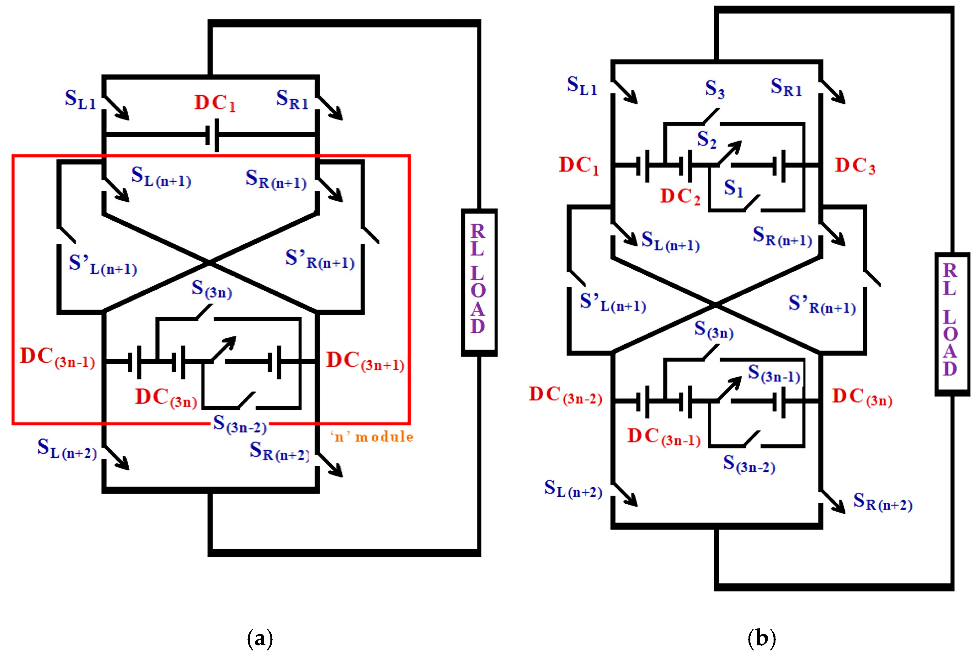
The proposed triple-source reduced-component multilevel inverter (RCC-MLI) introduces a simplified modular structure that generates multiple output voltage levels using a minimum number of semiconductor devices and DC sources. The main feature of this topology is the use of three DC sources (DC1, DC2, and DC3) connected through a cross-linked configuration that allows additive and subtractive voltage synthesis without relying on clamping capacitors or multiple isolated supplies. The resulting architecture is capable of producing both symmetrical and asymmetrical voltage levels, which makes it highly flexible for integration into renewable energy and electric drive systems.
Here, Figure 1 illustrates the general configuration of the proposed MLI. Each module consists of a combination of unidirectional and bidirectional switches, where the bidirectional devices (S′L and S′R) enable reverse current conduction under inductive load conditions. The ladder-structured connection permits voltage level generation by selective activation of these switches, forming distinct current conduction paths for each output state.
Figure 1. (a,b) Overall circuit configuration of the proposed triple-source reduced-component-count (RCC) multilevel inverter (MLI). Three isolated DC sources (DC1, DC2, and DC3) are connected through a cross-linked bridge structure using unidirectional and bidirectional switches to generate multiple output voltage levels with a reduced component count.

2.1. Voltage Level Generation Mechanism

The output voltage levels are synthesized by controlling the conduction sequence of the switches associated with each DC source. For every level, only four switches conduct simultaneously, thus reducing conduction losses. The sequence ensures that unidirectional current flows through the load without circulating among DC sources.
The voltage levels and corresponding switch combinations are summarized as follows:
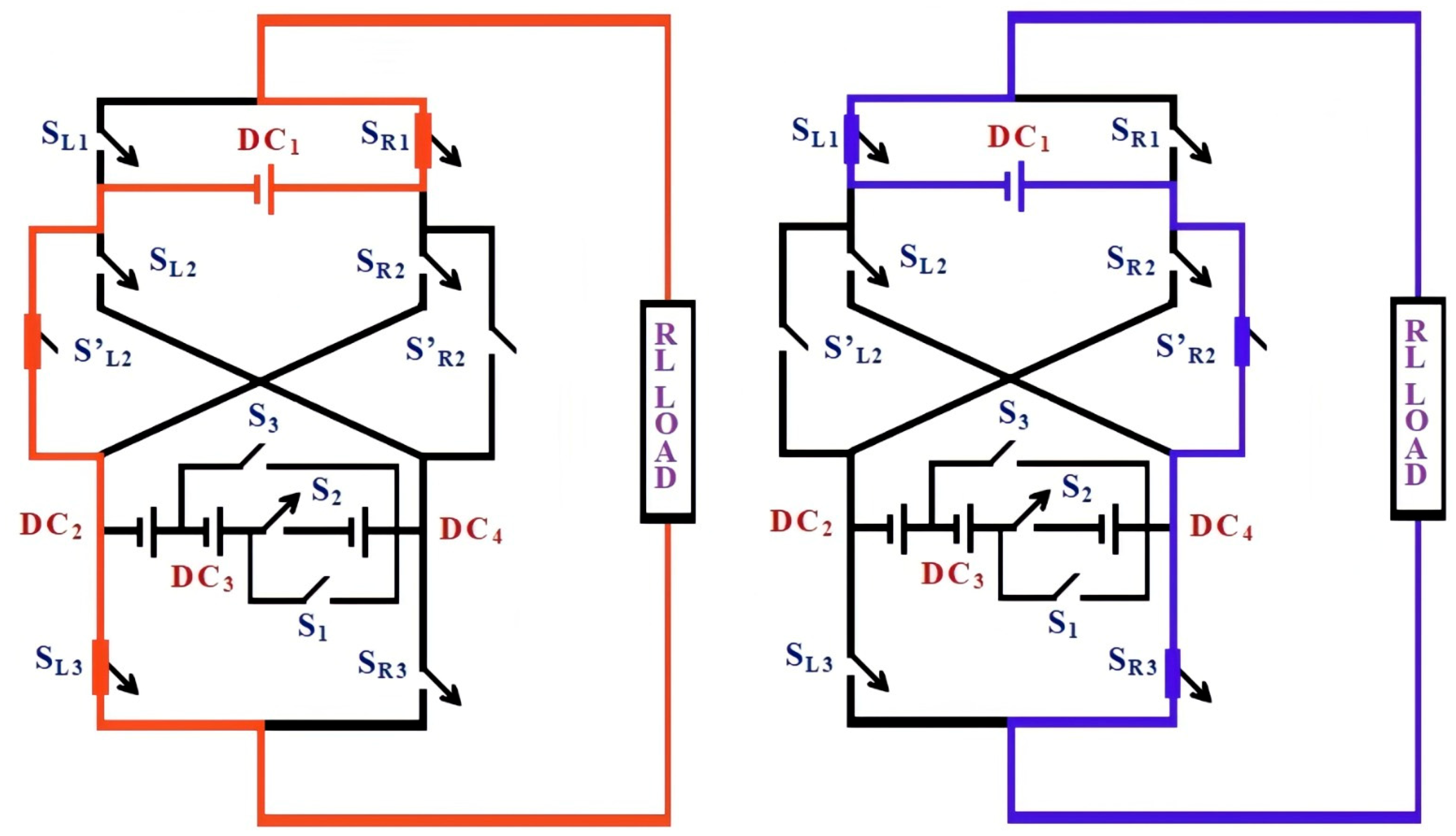
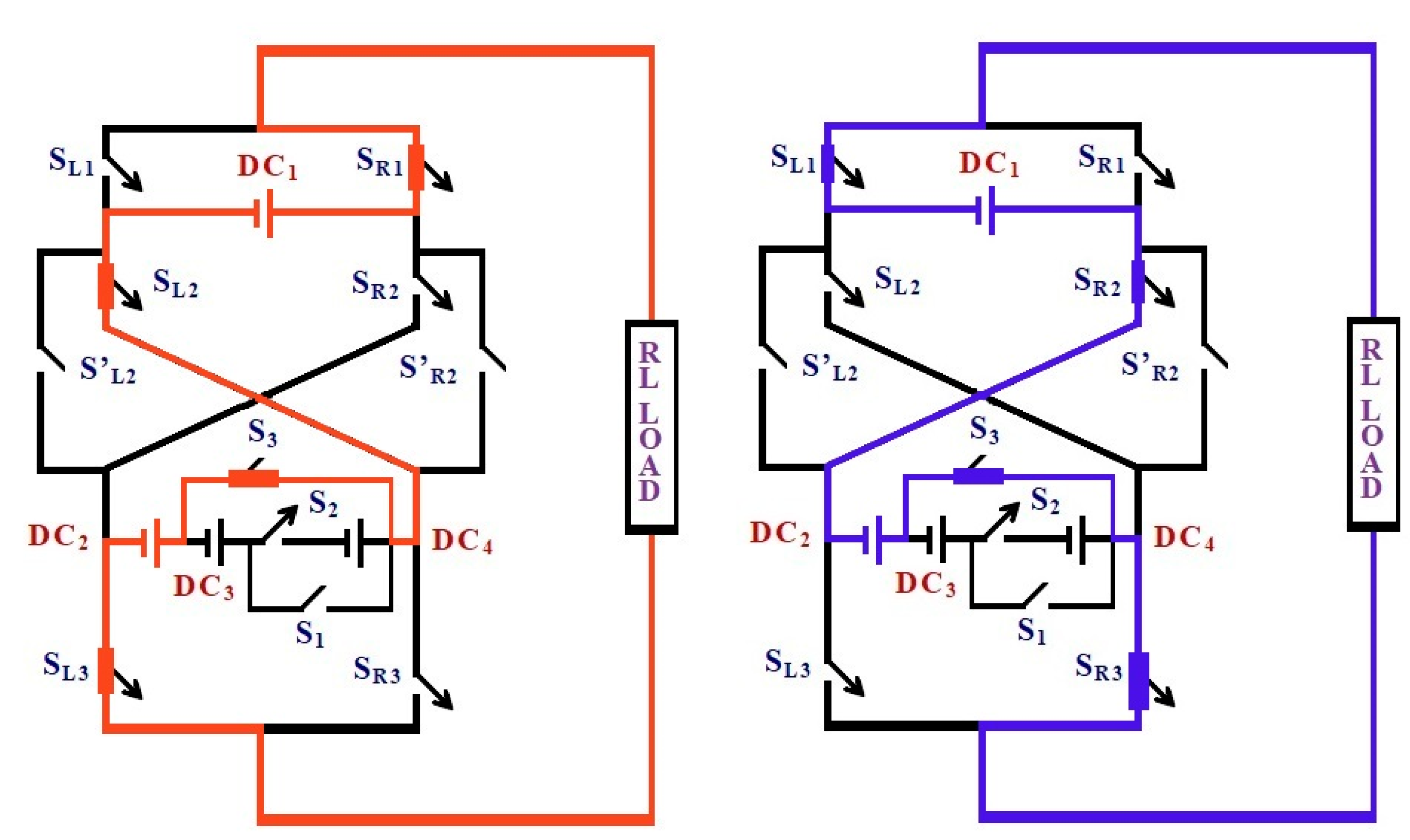
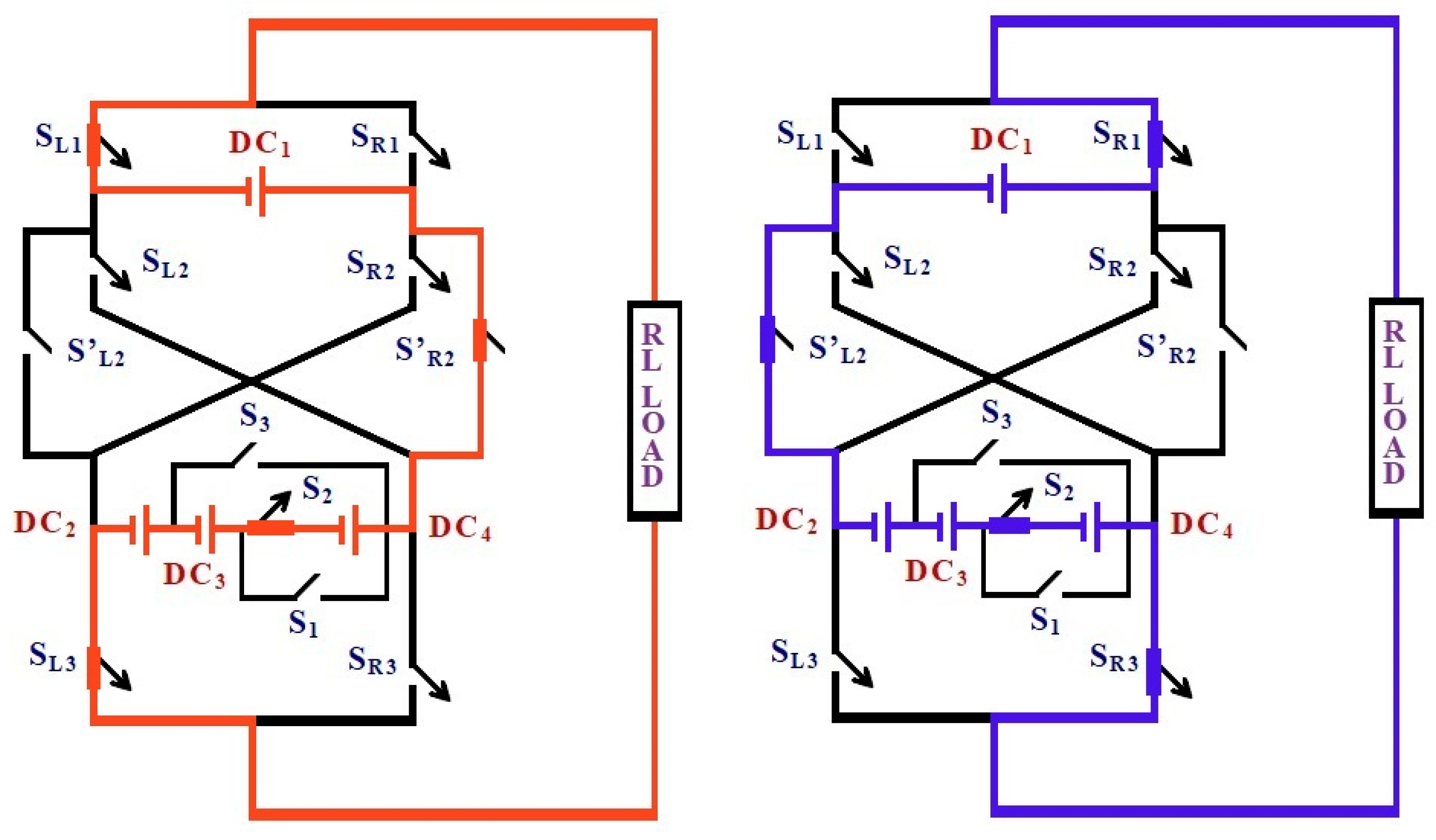
  • For the minimum output level (+VDC1), switches SR1, S′L2, and SL3 conduct, establishing a current path through DC1.
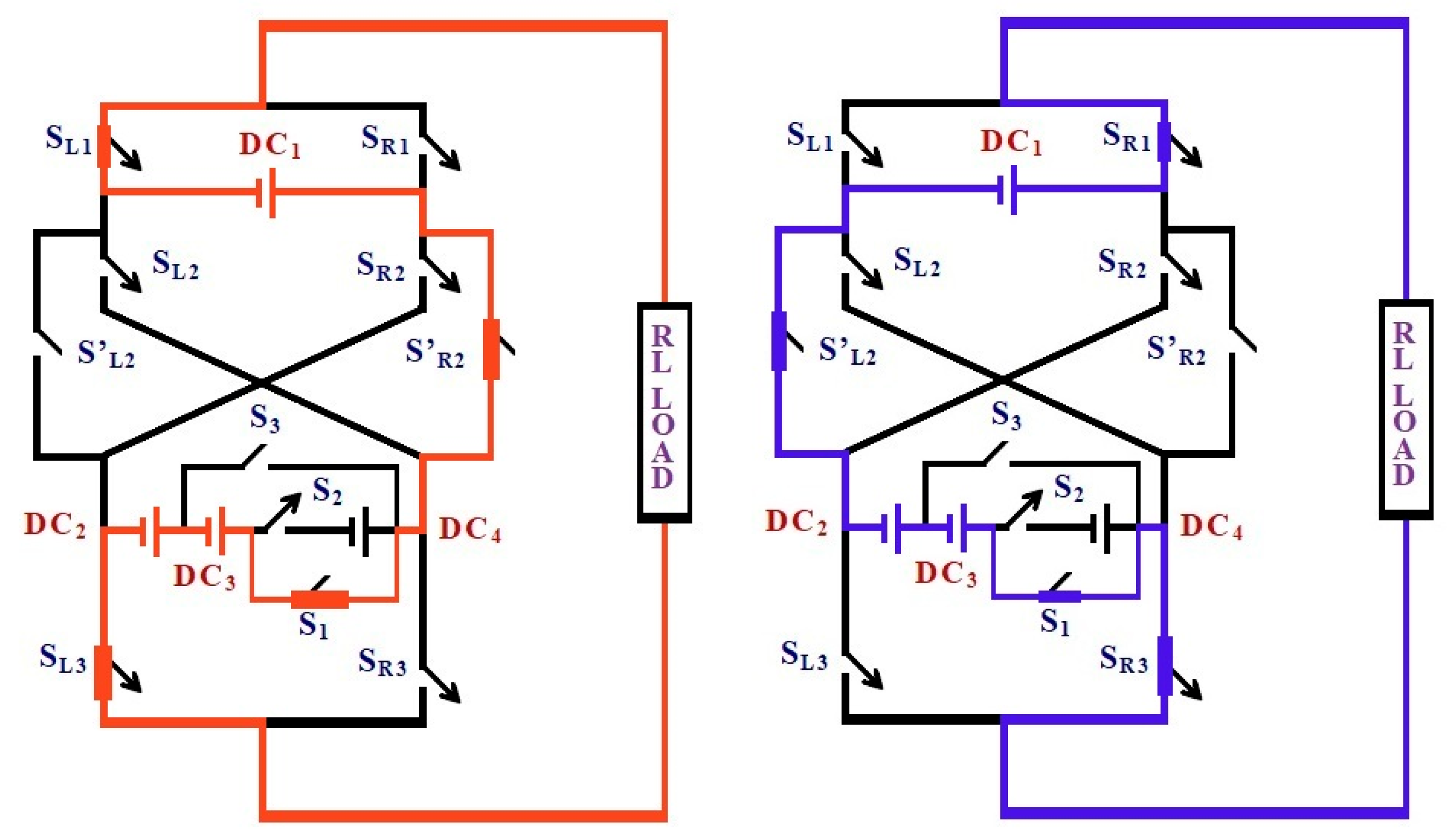
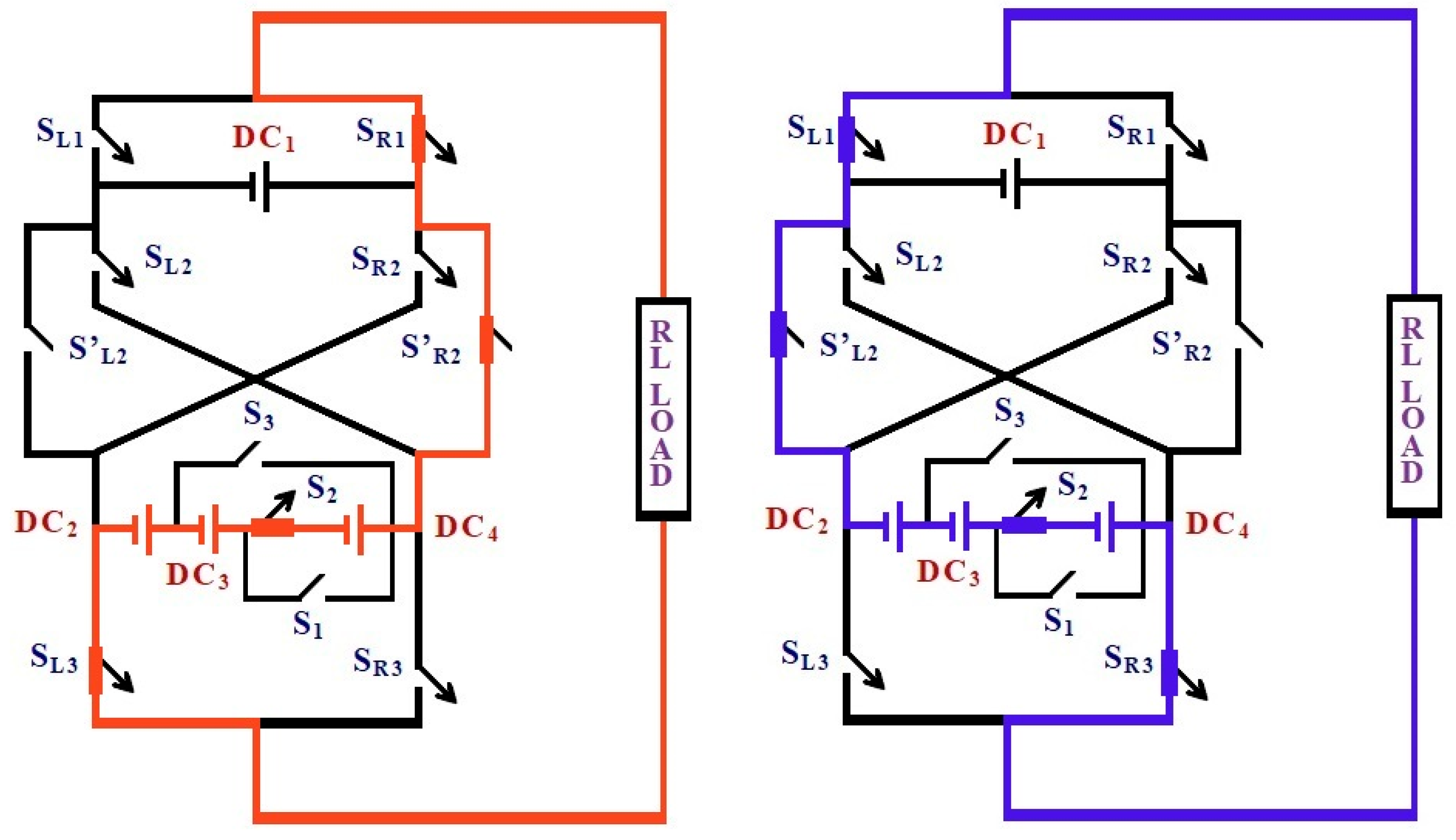
  • For the intermediate level (+VDC2 − VDC1), switches SR1, S′L2, SR3, and S3 are ON, connecting DC2 while isolating DC1.
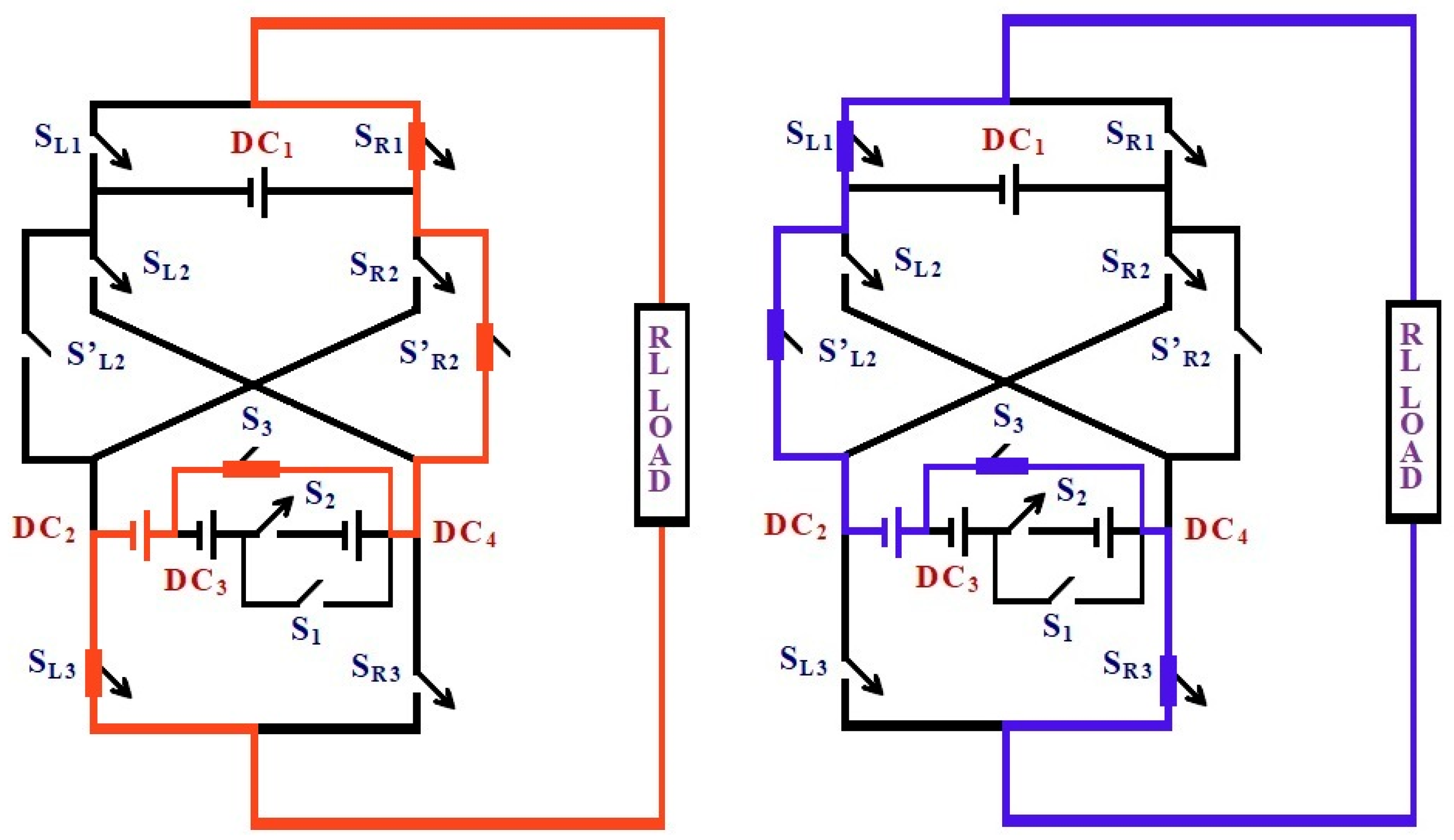
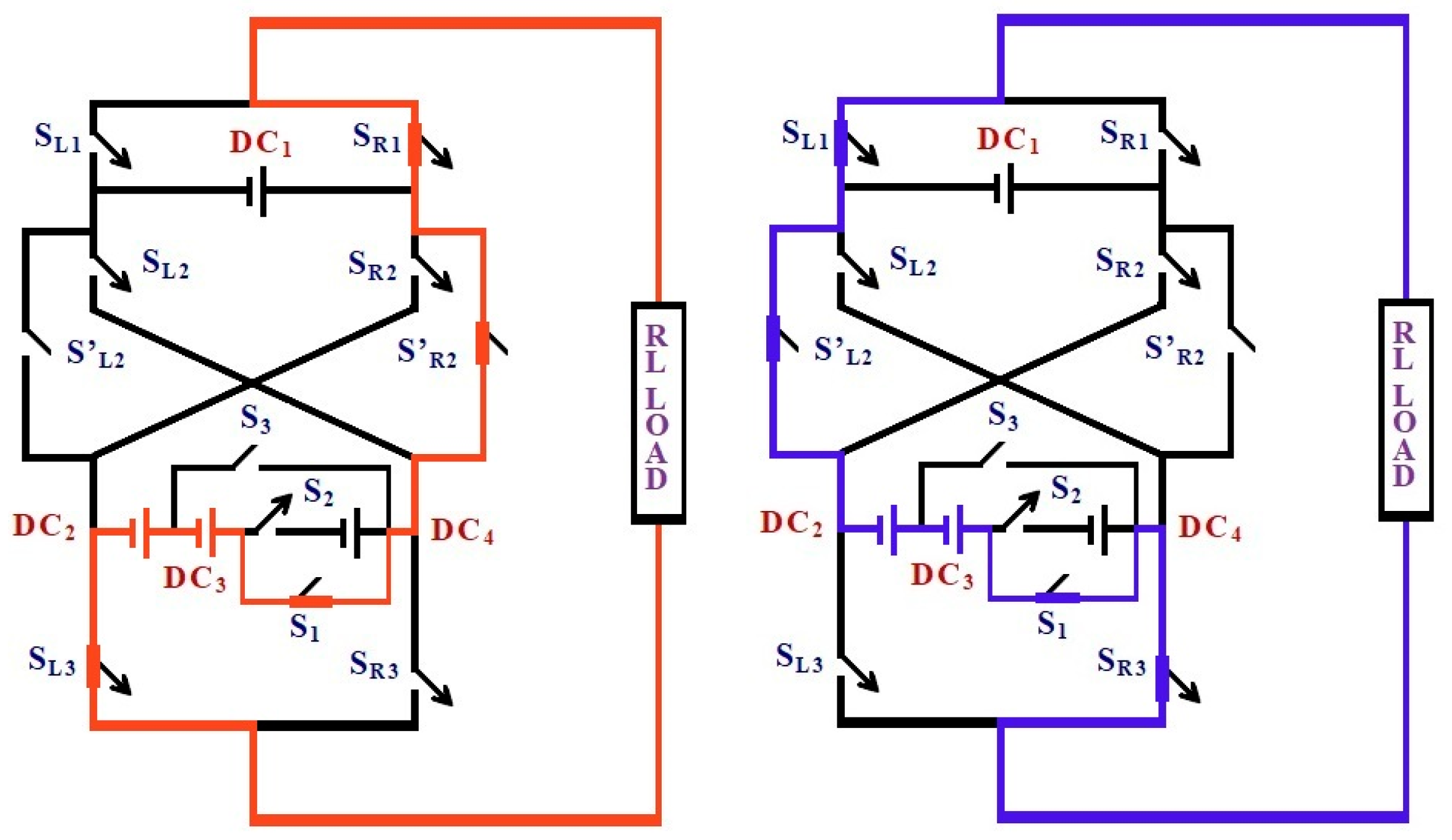
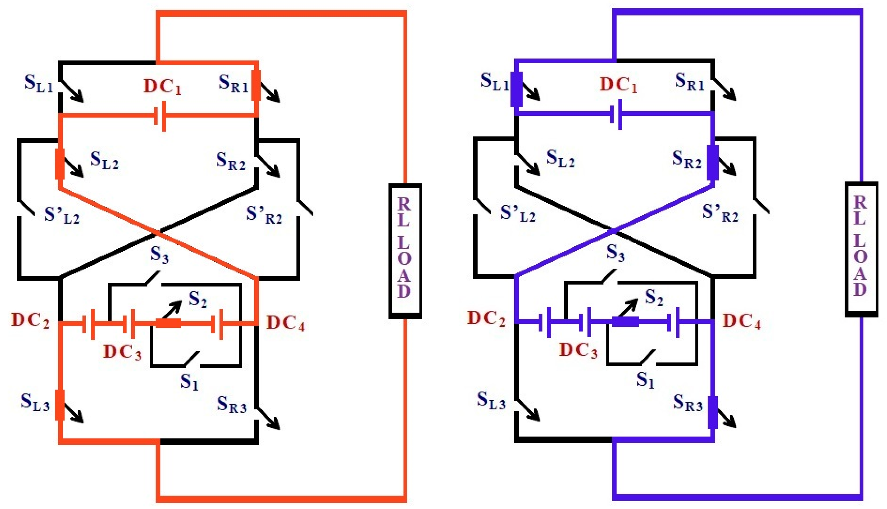
  • For the next higher level (+VDC2 + VDC3 − VDC1), switches SR1, S′R2, SL3, and S1 conduct, allowing additive synthesis of the DC2 and DC3 voltages.
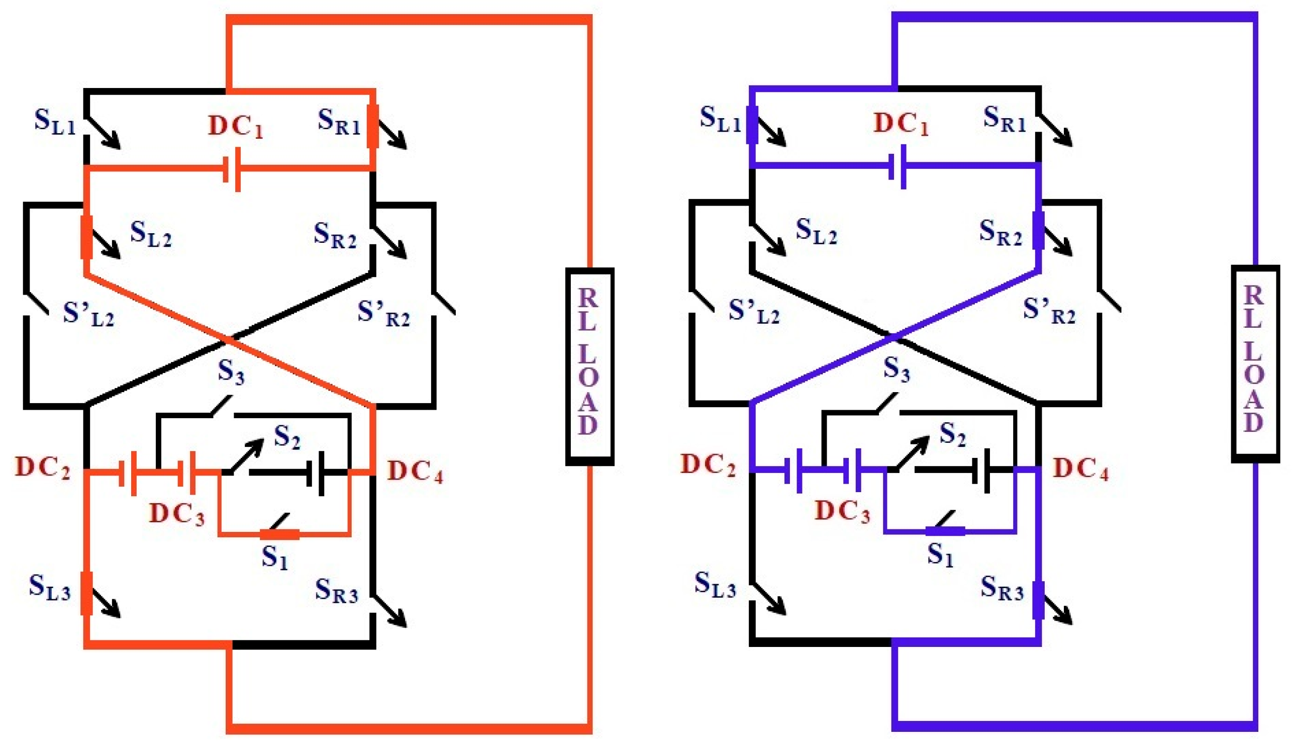
  • For the maximum level (+VDC1 + VDC2 + VDC3), switches SR1, S′R2, SR3, and S1 are ON, yielding the full triple-source voltage output.
During negative half-cycles, the corresponding switches on the opposite leg operate in a complementary manner to generate the negative voltage levels. The conduction paths for all these states are illustrated in revised Figures 3–12, where current directions are clearly marked with arrows. For better clarity, each voltage step from figures mentioned above includes the corresponding switch combination and load current direction. The conduction paths are sequentially discussed to illustrate the physical behavior of the current through the load at every voltage level.

2.2. Current Conduction Paths and Inductive Load Behavior

For inductive loads, where the current lags the voltage, current continuity is ensured by the bidirectional switch configuration and the anti-parallel diodes connected across all IGBTs. When a switch is turned OFF, the associated freewheeling diode momentarily conducts, maintaining current flow through the load and preventing voltage overshoot. This arrangement guarantees smooth current commutation and eliminates abrupt interruptions, as validated by the experimental waveforms shown in revised Figures 21 and 24. A representative R–L load is integrated in all switching states (Figures mentioned above), where current continuity is maintained through bidirectional switches and anti-parallel diodes. This ensures an uninterrupted current even during voltage polarity reversal.

2.3. Voltage and Current Stress Across Switches

To accurately estimate the conduction and switching losses, the voltage and current stresses across each semiconductor device were analytically derived. The maximum blocking voltage for each device is expressed as
SL1 = SR1 = DC(3n−2) + DC(3n−1) + DC(3n); n ≥ 1
Here, V m represents the peak amplitude of the desired fundamental voltage, T denotes the total period of the sinusoidal waveform, E is the DC source voltage, δ k indicates the pulse width corresponding to the k t h   segment, and S S refers to the switching state determining the active voltage level during each interval.
S(3n−1) = S(3n−2) = DC(3n)
S(3n) = DC(3n−1)+ DC(3n); n ≥ 1
S L ( n + 1 ) = S L ( n + 1 ) = S R ( n + 1 ) = S R ( n + 1 ) = j = 1 n 1 DC j + [ DC ( 3 n 2 ) + DC ( 3 n 1 ) + DC ( 3 n ) ]
SL(n+2) = SR(n+2) = [DC(3n − 2) + DC(3n − 1) + DC(3n)]; n ≥ 1
These relationships confirm that the maximum voltage stress experienced by any switch does not exceed approximately 45% of the total DC-link voltage, ensuring reduced device stress and improved reliability.
The current through each conducting switch equals the instantaneous load current (Iload), since only four devices conduct at a time. Therefore, the conduction loss for each device is calculated as
P c o n d = I r m s 2 × R o n Watts
and the total conduction loss per cycle becomes
P c o n d ( t o t a l ) = 4 × I r m s 2 × R o n Watts
Power loss analysis: The power loss can be estimated from the characteristic curves of the devices available in the datasheets. The power loss calculation includes conduction and switching losses. The selected IGBTs (IRG4BC20SD) are subjected to a maximum forward current of 19 A and a direct voltage of 600 V. The characteristic curves are Vsat(θ) × Il(θ) and E(θ) × Il(θ), where Vsat is the ON-state saturation voltage (Vce(θ) for the IGBT and VF(θ) for the diode), and E(θ) represents the energy loss during a single commutation (EON(θ) is a turn-ON commutation, EOFF (θ) the turn-off commutation, and Erec(θ) is owed for the diode reverse recovery process). The curves are approximated by the exponential in (9) to (14) using the curve-fitting tool available in MATLAB 2018. The mathematical models obtained for the IGBTs are given by
V c c = 0.96 e 0.0016 I 1 θ 0.4654 e 0.011 I 1 ( θ )
V F = 0.6 e 0.002 I 1 θ 0.4258 e 0.0275 I 1 ( θ )  
E r e c = 0.000806 e 0.000322 I 1 θ 0.0057 e 0.0446 I 1 ( θ )
E O N = 0.00041 e 0.0044 I 1 θ 0.0037 e 0.008 I 1 ( θ )
E o f f = 0.0443 e 0.00021 I 1 θ 0.00547 e 0.0107 I 1 ( θ )
I 1 θ = I m a x ( s i n ( θ φ ) )
where Il(θ) is the load current, and j is the load–displacement angle.
The switching loss occurs during turn-ON and turn-OFF, and for every power device (Psw), it is obtained by identifying the corresponding turn-ON and turn-OFF instants during one reference period by using (14), as follows:
P s w = 1 T ( E O N + E O F F + E r e c )  
The current is computed by multiplying the ON-state voltage by the ON-state current. The calculation of conduction losses for each semiconductor device using (15) to (16) is given by
P c o n T = 1 2 π 0 2 π V c c θ I 1 θ d θ  
P c o n T = 1 2 π 0 2 π V F θ I 1 θ d θ

2.4. Switching Loss Minimization

The carrier-less hybrid PWM strategy used in this topology minimizes switching losses by reducing the number of transitions per fundamental cycle. Each device switches only when the current crosses zero or at controlled angles derived from the equal-area criterion, expressed as
P s w = 1 2 V s w I s w ( t o n + t o f f ) f s w
By lowering the effective switching frequency and synchronizing turn-ON/turn-OFF events with current zero crossings, the proposed method significantly reduces the total switching energy dissipation.
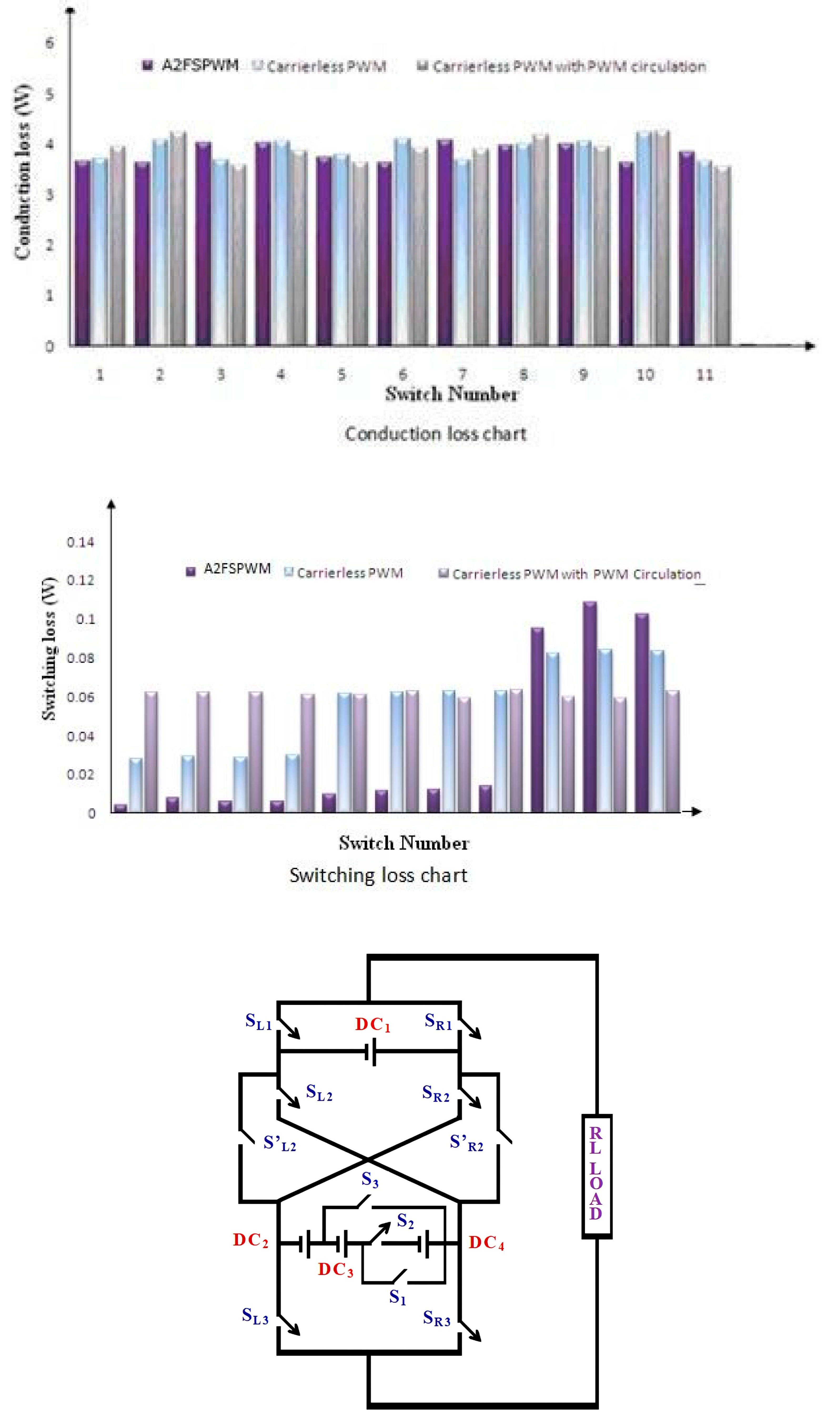
The blocking voltage and current conduction through each switch were analyzed to determine the power losses in the proposed inverter. Each device sustains only a portion of the total DC-link voltage, as derived in Equations (1)–(5), effectively reducing voltage stress. During operation, only four switches conduct at a time, and each carries the same load current. Consequently, both conduction and switching losses are minimized due to reduced current paths and fewer transitions per cycle under the hybrid PWM strategy (Figure 2).
Figure 2. Circuit diagram of the proposed 21-level RCC-MLI using three DC sources and cross-connected switches for voltage synthesis.
Each voltage level in the proposed 21-level inverter is synthesized through controlled activation of specific switch pairs on the left and right arms of the ladder-structured triple-source module. For each voltage step, only four switches are in the conducting state, establishing distinct current conduction paths between the selected DC sources and the load. Figure 3, Figure 4, Figure 5, Figure 6, Figure 7, Figure 8, Figure 9, Figure 10, Figure 11 and Figure 12 illustrate these conduction paths for both polarities, where the current direction is indicated by arrows. This switching pattern ensures a unidirectional current flow, minimizes device stress, and results in reduced conduction losses while producing symmetric stepped voltage levels.
Figure 3. Switching state for the output voltage level ± DC1. Current conduction path for output level +VDC1. Switches SR1, S′L2, and SL3 are turned ON, establishing the current flow through DC1 and the load. The remaining switches are OFF, ensuring minimal conduction loss. Red color flow (left diagram) denotes the current conduction path for the positive output voltage level (+VDC1). Blue color flow (right diagram) denotes the current conduction path for the negative output voltage level (−VDC1).
Figure 4. Switching state for the output voltage level ± (DC2−DC1) and the conduction path for the output level + VDC2 − VDC1. Switches SR1, S′L2, SR3, and S3 are ON, connecting DC2 to the load while isolating DC1. This configuration produces an intermediate positive voltage level. Red color flow (left diagram) denotes the current conduction path for the positive output voltage level (+VDC1). Blue color flow (right diagram) denotes the current conduction path for the negative output voltage level (−VDC1).
Figure 5. Switching state for the output voltage level ± DC2. In this mode, switches SR1, SR2′, SL3, and S1 conduct to synthesize an additive voltage of +VDC2 + VDC3 − VDC1 across the load. Red color flow (left diagram) denotes the current conduction path for the positive output voltage level (+VDC1). Blue color flow (right diagram) denotes the current conduction path for the negative output voltage level (−VDC1).
Figure 6. Switching state for the output voltage level ± (DC2 + DC1). Current conduction path for maximum output level +VDC1 + VDC2 + VDC3. Switches SR1, S′R2, SR3, and S1 are ON, providing the full positive peak voltage. This state represents the highest energy conversion point. Red color flow (left diagram) denotes the current conduction path for the positive output voltage level (+VDC1). Blue color flow (right diagram) denotes the current conduction path for the negative output voltage level (−VDC1).
Figure 7. Switching state for the output voltage level ± (DC2 + DC3 − DC1). Conduction path for zero (neutral)-voltage level. The complementary leg switches S′L and S′R operate simultaneously, forming a short-circuited current loop within the inverter, maintaining load current continuity without producing an output voltage. Red color flow (left diagram) denotes the current conduction path for the positive output voltage level (+VDC1). Blue color flow (right diagram) denotes the current conduction path for the negative output voltage level (−VDC1).
Figure 8. Switching state for the output voltage level ± (DC2 + DC3) and current conduction path for the negative voltage level −VDC1. The corresponding lower-leg switches SL1, S′R2, and SR3 are ON. The load current flows in the reverse direction through DC1 and anti-parallel diodes, ensuring a symmetrical negative output. Red color flow (left diagram) denotes the current conduction path for the positive output voltage level (+VDC1). Blue color flow (right diagram) denotes the current conduction path for the negative output voltage level (−VDC1).
Figure 9. Switching state for the output voltage level ± (DC2 + DC3 + DC1) and conduction path for negative intermediate level −(VDC2 − VDC1). Switches SL1, S′R2, SL3, and S3 are ON, connecting DC2 in reverse polarity relative to the load. Red color flow (left diagram) denotes the current conduction path for the positive output voltage level (+VDC1). Blue color flow (right diagram) denotes the current conduction path for the negative output voltage level (−VDC1).
Figure 10. Switching state for the output voltage level ± (DC2 + DC3 + DC4 − DC1) and conduction path for −(VDC2 + VDC3 − VDC1). Switches SL1, S′L2, SR3, and S1 conduct, producing the additive negative level across the load. Red color flow (left diagram) denotes the current conduction path for the positive output voltage level (+VDC1). Blue color flow (right diagram) denotes the current conduction path for the negative output voltage level (−VDC1).
Figure 11. Switching state for the output voltage level ± (DC2 + DC3 + DC4) and switching configuration for the maximum negative level −(VDC1 + VDC2 + VDC3). Switches SL1, S′L2, SL3, and S1 are ON. This represents the mirror image of the highest positive level. Red color flow (left diagram) denotes the current conduction path for the positive output voltage level (+VDC1). Blue color flow (right diagram) denotes the current conduction path for the negative output voltage level (−VDC1).
Figure 12. Switching state for the output voltage level ± (DC2+ DC3+ DC4+ DC1) and generalized switching sequence diagram summarizing all conduction states of the proposed RCC-MLI for one fundamental cycle. The figure highlights symmetry between positive and negative half-cycles and the reduced number of active switches per step (only four at any time). Red color flow (left diagram) denotes the current conduction path for the positive output voltage level (+VDC1). Blue color flow (right diagram) denotes the current conduction path for the negative output voltage level (−VDC1).
The proposed RCC-MLI produces stepped output voltage levels based on the number of DC input sources and switching combinations (Table 1 and Table 2). Each configuration incrementally adds voltage stages by summing available DC magnitudes, as summarized in Table 1.
Table 1. Relations for computing the magnitude value of DC voltage source.
Table 2. Switching states and conducting devices of the proposed 21-level RCC-MLI.
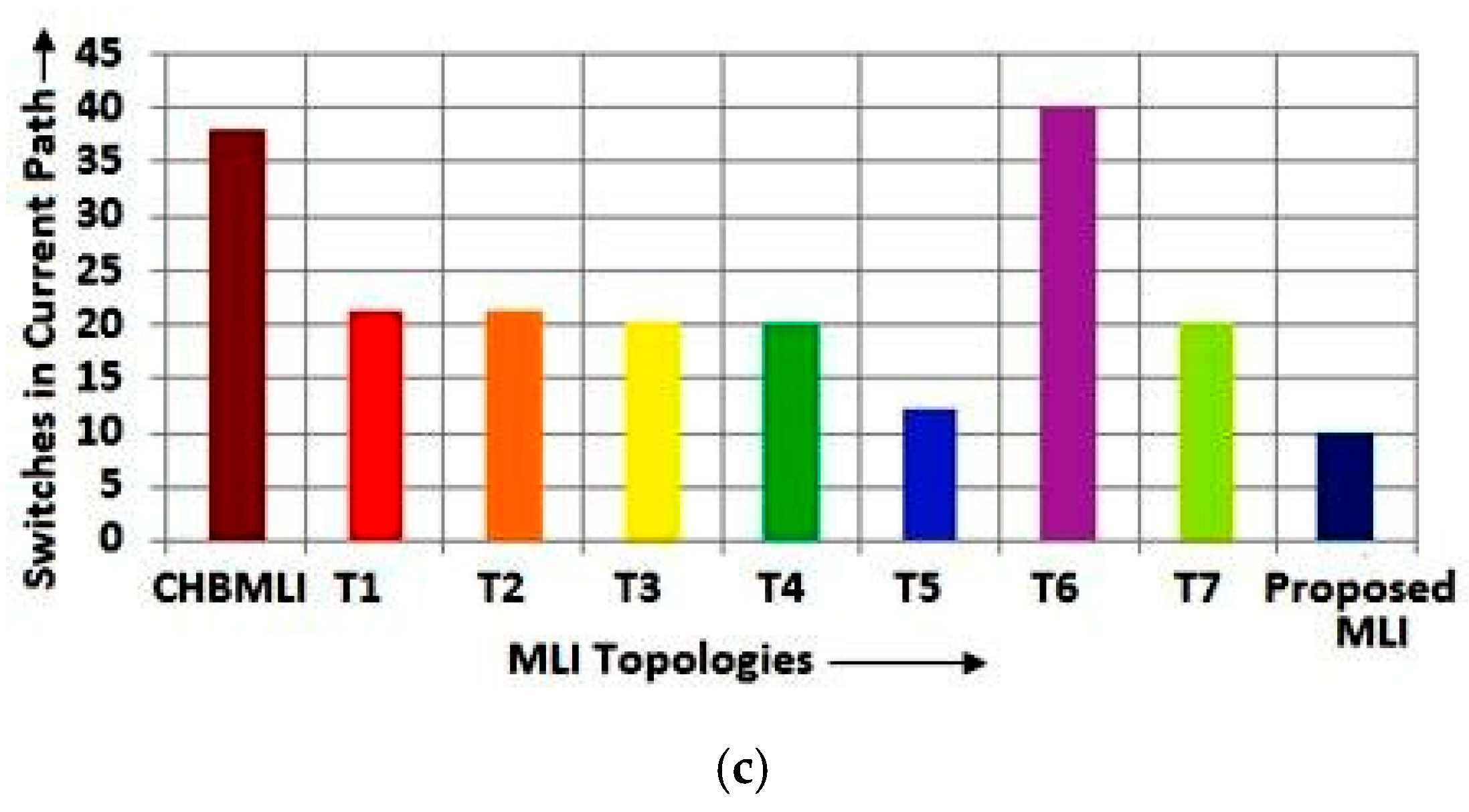
The practicality of the proposed algorithm is evidenced by a detailed comparison of switch count, gate drivers, and conducting current paths. It is also compared with CHBMLI and other recently developed reduced-component topologies, which are cited in references [,,,,,,,], thus revealing the impact of the algorithm on the execution of the tasks in the field. Figure 13 displays the graphs for the need of the switches along with the gate drivers and the current-conducting switches to build a 75-level inverter.
Figure 13. Comparison chart in terms of (a) switches, (b) gate drivers, and (c) current-conducting switches for a 75-level inverter.
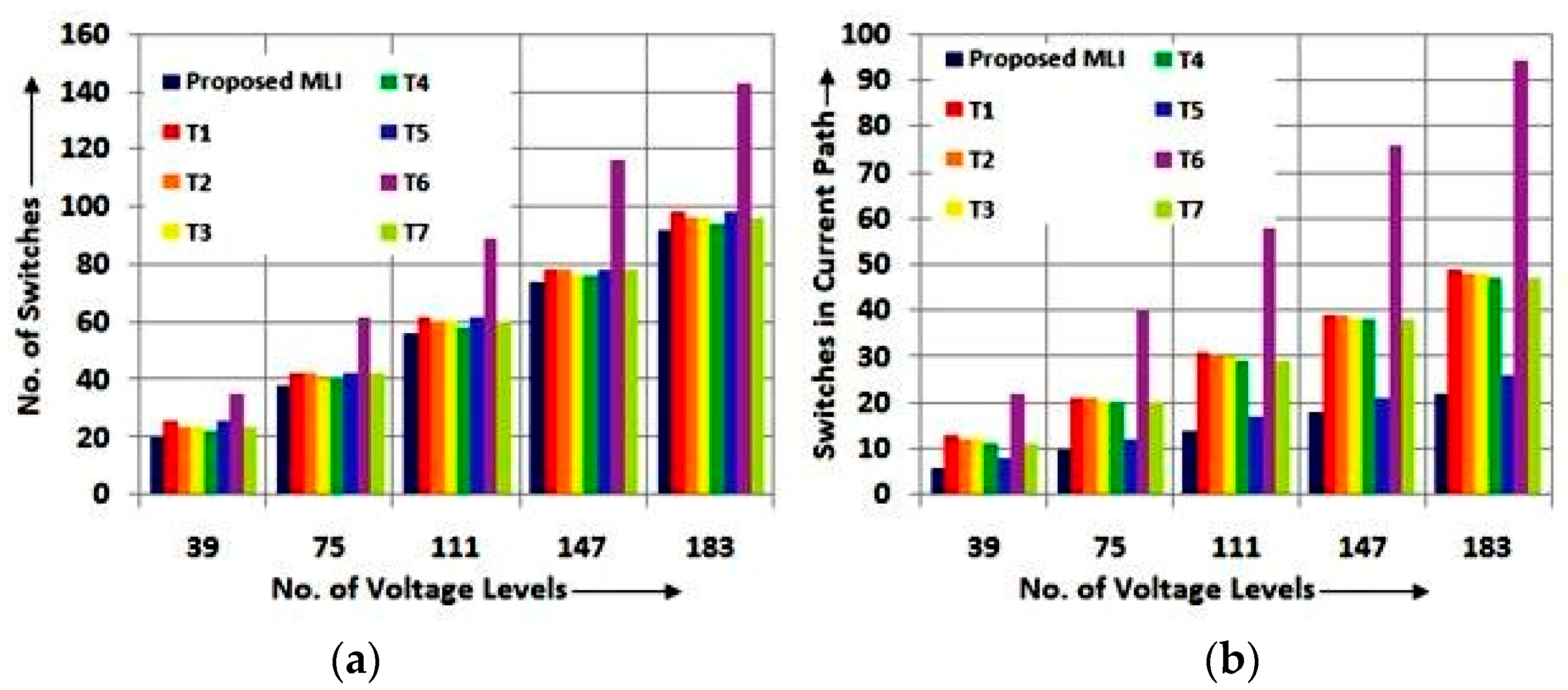
Based on Figure 14b, only four switches conduct at any instant, reducing switching losses and simplifying control. The proposed inverter employs bidirectional switches realized through two IGBTs connected in a common-emitter configuration. This arrangement enables current conduction in both directions, ensuring continuous current flow through the load even during polarity transitions. Compared with conventional unidirectional switches used in cascaded H-Bridge MLIs, this configuration eliminates the need for additional anti-parallel diodes or commutation circuits, simplifying design and reducing switching losses. Moreover, bidirectional implementation ensures faster current reversal and enhanced reliability under inductive-loading conditions.
Figure 14. Comparison chart in terms of (a) switches and (b) current-conducting switches for variations in voltage levels.
Likewise, Figure 14 sketches the comparison chart between the proposed algorithm and recent reduced-count topologies against changes in the count of voltage levels. It is confirmed from Figure 13 and Figure 14 that fewer power components are needed by the proposed topology.

3. Proposed Hybrid PWM Strategy

The proposed control technique is based on pulse-width modulation (PWM) rather than pulse-position modulation (PPM). It employs a carrier-less hybrid PWM framework derived from the equal-area criterion, specifically optimized for the triple-source reduced-component-count multilevel inverter (RCC-MLI) topology. In this method, the width of each pulse is analytically computed, such that the area under the pulse equals the area of the corresponding segment of the sinusoidal reference waveform. This ensures accurate waveform synthesis, harmonic minimization, and precise digital implementation while avoiding carrier-based comparisons.
The primary objective of the proposed PWM mechanism is to generate modulation pulses for multilevel inverters without relying on conventional carrier or reference signals, thereby making it independent of the number of output voltage levels. The technique enforces that the average output voltage during each switching interval matches the corresponding section of the desired sinusoidal reference. The constant (square)-voltage component at each level is first subtracted from the desired fundamental voltage, leaving the remaining sinusoidal section to be reconstructed through PWM control. Each half-cycle is divided into discrete constant-voltage intervals, and calculated switching pulses are assigned to these intervals, such that the total area under each pulse matches that of the reference sine wave.
Unlike traditional multicarrier PWM, which depends on multiple triangular carriers and frequent commutations, the proposed carrier-less hybrid scheme determines switching instants directly from the crossing points of equal-area segments. This approach significantly reduces switching losses, simplifies digital realization, and maintains excellent waveform fidelity. Two hybrid modulation variants were developed, each employing different voltage-level selection (odd or even) to minimize total harmonic distortion (THD) while preserving the desired fundamental amplitude. The gating signals for all power devices are generated using a field-programmable gate array (FPGA)-based controller, which accesses pre-computed lookup tables derived from analytically determined switching angles. This digital realization guarantees precise timing synchronization and a close match between simulated and experimental waveforms. A fixed dead-time of 2 µs was implemented in the FPGA gating logic to avoid shoot-through conditions and minimize low-order harmonic distortion. The PWM generation module utilized approximately 1200 LUTs and 850 flip-flops on the Spartan-3E FPGA, operating at 50 MHz.

Novelty and Advantages of Proposed PWM Approach

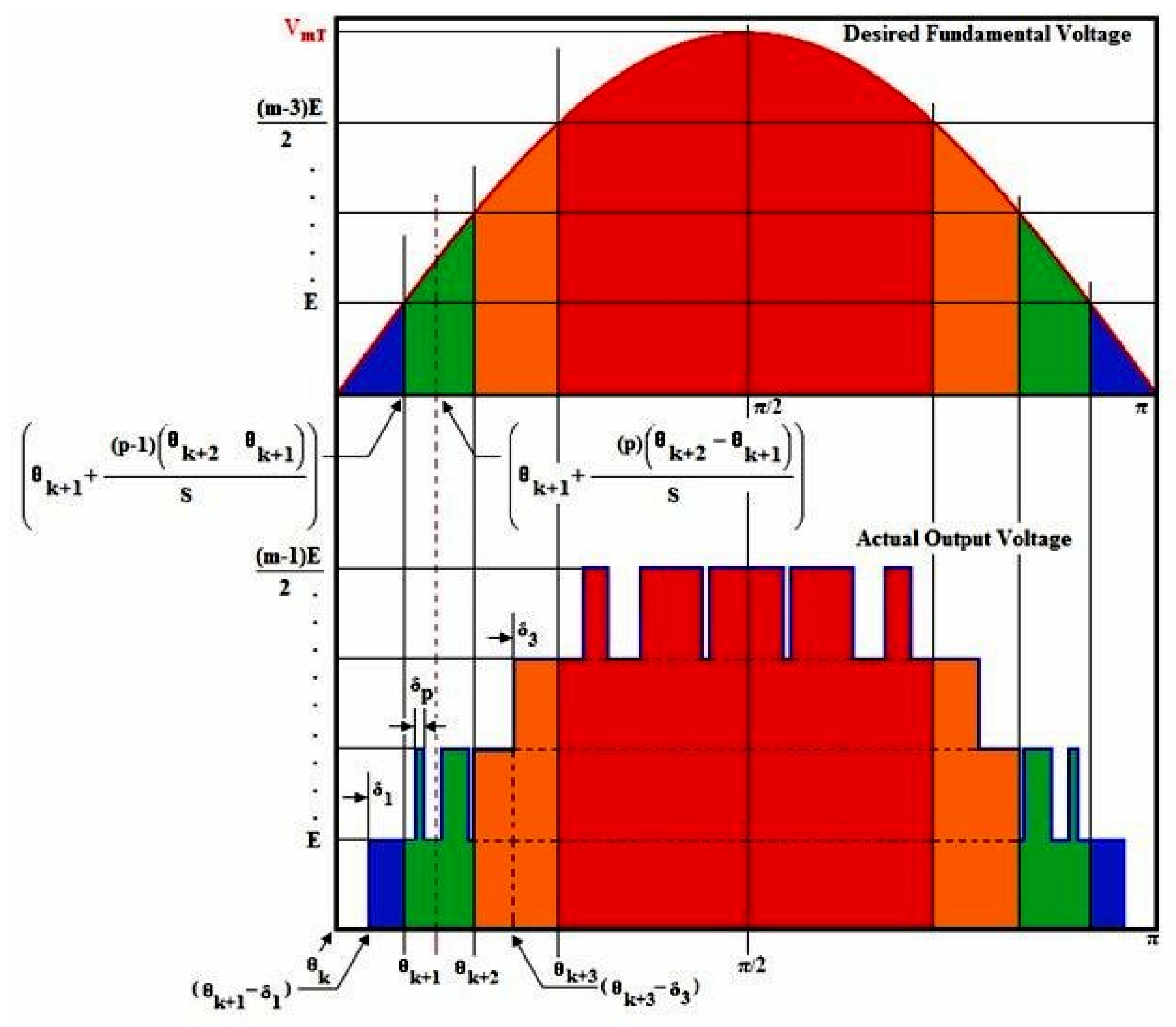
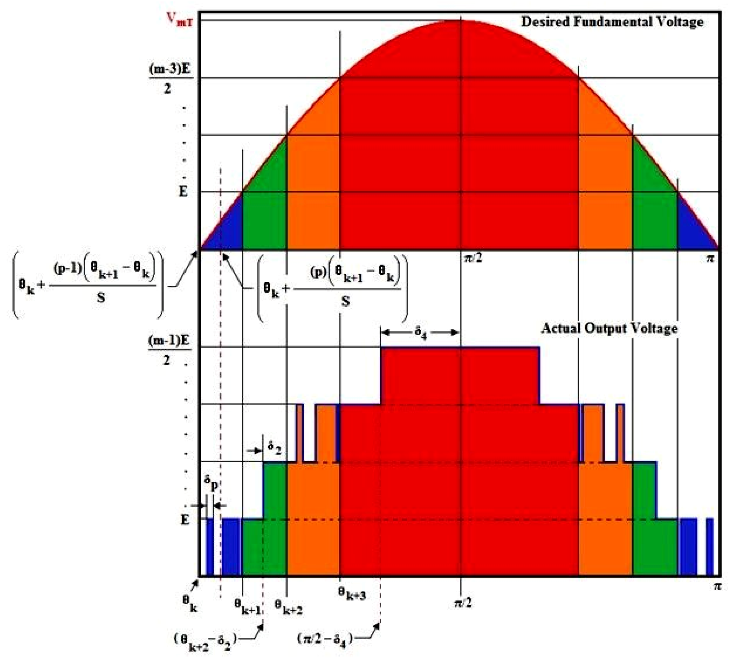
While the equal-area principle has been explored in classical sinusoidal and selective harmonic elimination PWM methods, the present work introduces a novel carrier-less hybrid PWM scheme specifically designed for a triple-source RCC-MLI. This hybrid carrier-less PWM framework achieves a lower switching frequency per device, enhanced harmonic performance, and simplified digital control compared with conventional carrier-based PWM schemes. It effectively extends the equal-area principle into a practical, high-efficiency modulation method suitable for reduced-component-count multilevel inverter structures (Figure 15 and Figure 16).
Figure 15. Hybrid PWM strategy-amalgamated AEFSPWM.
Figure 16. Hybrid PWM strategy-amalgamated FSAEPWM.
The fundamental sine wave is vertically divided into ‘m’ constant stages with voltage magnitude (E). The intersecting point of the fundamental sine wave and the DC voltage determines the cross-over point (θ1, θ2…π/2). The non-linear portion is horizontally sampled [(S−1)/2] to achieve PWM pulses (p) in each quarter-cycle. For a nine-level inverter, the cross-over points are (θ1, θ2, θ3, and π/2), and the PWM occurs in the segments (0, θ1), (θ1, θ2), (θ2, θ3), and (θ3, π/2), while the square-wave portion in each level, including (π− θ1), (π− θ2), and (π− θ3), remains constant in that corresponding level because the area of both the desired and actual voltage are equal. Method I uses fundamental changing in odd levels and PWM in even levels of the output voltage, while Method II operates vice versa to Method I. Two distinct operational modes are defined in the proposed hybrid PWM scheme:
  • Method I—fundamental changing mode: Low-frequency switching is applied to generate primary voltage steps corresponding to major transitions in the output waveform. This mode minimizes switching losses and establishes the base fundamental component.
  • Method II—PWM mode: Within each fundamental interval, the equal-area-based PWM pulses are generated to refine waveform linearity and suppress harmonic content. This hybridization allows reduced THD while maintaining high efficiency.
Pulse rotation is applied in both methods to improve the output voltage quality by reducing harmonics and enhancing waveform symmetry.
The crossing instant between the fundamental sine with magnitude (VmT) and the actual output voltage with each level (k) at the voltage of (E) is
V mT × Sin ( θ k + 1 ) = K × E θ k + 1 = Sin 1 K × E V mT
where k = 1 , 2 m 1 2 .
The duty cycle for fundamental changing is computed as follows.
The area of the desired fundamental sine voltage is given by
Desired k ( p ) = θ k θ k + 1 V mT sin ω t d ω t ( i × E ) θ k + 1 θ k
Desired k ( p ) = V mT cos θ k cos θ k + 1 i × E θ k + 1 θ k
Desired k ( p ) = 2 V mT sin θ k + θ k + 1 2 × sin θ k + 1 θ k 2 i × E θ k + 1 θ k
The area of the actual output voltage is given by
Actual k p = δ k × E Actual k p = Desired k P δ k ( p ) = 2 V mT E sin θ k + θ k + 1 2 × sin θ k + 1 θ k 2 i θ k + 1 θ k
The duty cycle for PWM is computed as follows.
The rising and falling instant of each sample (p) is given by
Rising   edge k p = a = θ k + p 1 θ k + 1 θ k S ;   P = 1 , 2 S
Falling   edge k p = b = θ k + p θ k + 1 θ k S ;   P = 1 , 2 S
Desired k ( p ) = a b V mT sin ω t d ω t ( i × E ) θ k + 1 θ k S
Desired k ( p ) = V mT cos a cos b i × E θ k + 1 θ k S
Desired k ( p ) = 2 V mT sin θ k + p 0.5 θ k + 1 θ k S × sin θ k + 1 θ k 2 S i × E θ k + 1 θ k S
The area of the actual output voltage is given by
Actual k p = δ k × E Actual k p = Desired k P δ k ( p ) = 2 V mT E sin θ k + p 0.5 θ k + 1 θ k S × sin θ k + 1 θ k 2 S i θ k + 1 θ k S
where, i = (k−1) and k is the Kth level modulated either by fundamental changing (p = 1) or PWM (p = 1, 2…S), respectively.
Equations (1)–(20) collectively define the analytical computation of pulse widths and switching instants. Each pulse width δ k is determined such that the integral of the modulated voltage over a switching period equals that of the reference sine-wave segment. This process ensures an equal area under both curves, effectively reproducing the fundamental sinusoidal voltage while suppressing higher-order harmonics.

4. Analytical and Power Quality Analysis

The analytical validation of the proposed hybrid carrier-less PWM strategy establishes its ability to minimize low-order harmonics, enhance fundamental voltage utilization, and thereby improve overall power quality. The following derivations and discussions quantify these improvements and demonstrate the alignment between analytical, simulated, and experimental outcomes.

4.1. Fundamental Voltage Derivation

For an m-level inverter, the fundamental output voltage component can be derived from the Fourier expansion of the stepped waveform as
V 1 = 4 V d c π k = 1 m cos ( θ k )
where (θk) represents the switching angles determined by the equal-area condition that minimizes predominant low-order harmonics (third, fifth, and seventh) and maximizes the fundamental amplitude. In the proposed hybrid modulation, these angles are dynamically updated within the field-programmable gate array (FPGA) controller, ensuring waveform symmetry and a near-sinusoidal output voltage.

4.2. Total Harmonic Distortion (THD)

The total harmonic distortion (THD) is analytically expressed as
T H D = n = 2 V n 2 V 1 2
By substituting the calculated harmonic magnitudes obtained from Fourier analysis of the proposed waveform, the third and fifth harmonic components are observed to be less than 2.8%, while the seventh and higher harmonics remain below 1%. Hence, the overall total harmonic distortion (THD) is approximately 4.3%, which is a 40–45% reduction compared with conventional carrier-based PWM techniques (typically 7–8%). This analytical prediction closely agrees with the simulation and experimental spectra presented in Figures 26 and 31.

4.3. Fundamental Voltage Utilization and Efficiency

The proposed control approach enhances the effective fundamental voltage utilization to nearly 0.9 Vdc for a nine-level configuration, compared with 0.82 Vdc for standard sinusoidal PWM. As a result, the inverter delivers a higher RMS voltage to the load with reduced switching activity, leading to an increased overall conversion efficiency. The measured efficiency improvement is approximately 3–4% over comparable RCC-MLI structures.

4.4. Conduction and Switching Loss Analysis

The conduction loss per switch is given by Pcond = Irms2Ron, while the total conduction loss per cycle is
P c o n d t o t a l = 4 I r m s 2 R o n
where Irms is the RMS value of the current flowing through the device, and Ron is the on-state resistance of the IGBT/MOSFET. Since the proposed topology maintains a reduced number of conducting switches (Non = 4) per voltage level, the total conduction loss per cycle can be estimated as
P c o n d t o t a l = N o n × I r m s 2 × R o n
Compared with conventional cascaded H-bridge or NPC inverters where six to eight devices conduct simultaneously, the proposed configuration yields approximately a 40% reduction in conduction losses for an equivalent load and device parameters.
Additionally, the hybrid carrier-less PWM technique reduces switching transitions per fundamental cycle, thus lowering the overlap period during turn-ON and turn-OFF events, which further improves conversion efficiency. Switching loss reduction directly contributes to lower semiconductor heating and reduced need for external heat sinking, improving thermal efficiency.
The efficiency (η) of the inverter is now defined in the revised text as
η = P o u t P o u t + P c o n d ( t o t a l ) + P s w
The simulation results and experimental validation (Figures 29–35) confirm that the proposed inverter achieves a noticeable improvement in efficiency (≈95.2%) compared with conventional carrier-based PWM inverters (≈91.5%), primarily due to minimized conduction and switching losses.
Similarly, switching losses are minimized through the equal-area modulation technique, where the effective switching frequency is significantly lower than that of traditional multicarrier PWM. Substituting the practical switching parameters (Vsw = 100 V, Isw = 2 A, ton + toff ≈ 400 ns, and fsw = 2 kHz) yields an approximate switching loss reduction of 35%.
The conduction and switching losses are now derived based on the electrical characteristics of the selected IGBT device IRG4BC20SD. The conduction loss per switch is expressed as
P c o n d = i T 0 T V C E s a t i t . i t d t
where V C E ( s a t ) ( i ) is the current-dependent collector–emitter saturation voltage approximated by
V C E s a t i = a + b . i + c . i 2
with constants a = 0.7   V ,   b = 0.015   V / A ,     a n d   c = 0.0002   V / A 2 obtained through MATLAB curve fitting from the manufacturer’s datasheet.
The switching loss for each device is modeled as
P s w = f s w E o n + E o f f = f s w k 1 i s w V D C + k 2 i s w 2
where E o n   and E o f f   are the turn-ON and turn-OFF energies derived from empirical switching energy curves for IRG4BC20SD at V D C = 100   V   and I s w = 2   A . The constants k 1 = 3.6 × 10 6   and k 2 = 2.1 × 10 7   were determined experimentally.
The total power loss per cycle is then expressed as
P t o t a l = N o n . P c o n d + N s w . P s w
where N o n = 4   and N s w   represent the number of conducting and switching devices per fundamental cycle, respectively.
This refined analysis demonstrates that the total conduction and switching losses decrease by approximately 38–42% compared with conventional cascaded H-bridge MLIs.

4.5. EMI and Dynamic Performance

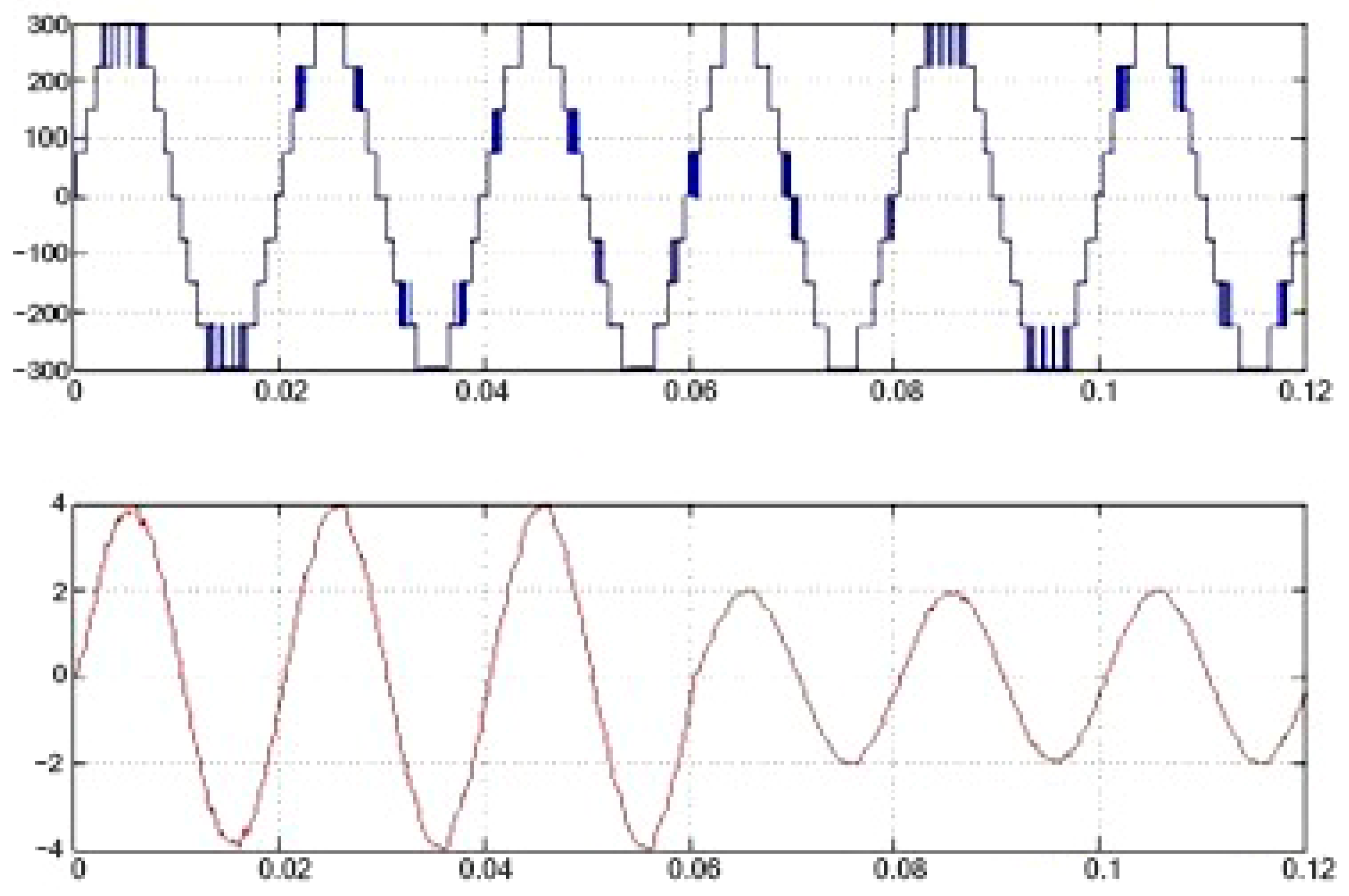
Because the proposed carrier-less strategy employs fewer transitions and smaller voltage steps per commutation, the rate of voltage change (dv/dt) is limited, thus suppressing electromagnetic interference (EMI). The symmetrical pulse placement ensures cancellation of common-mode voltages. Furthermore, field-programmable gate array (FPGA)-based real-time control enables near-instantaneous duty-cycle adjustments, enhancing dynamic response under sudden load variations. The FPGA-based closed-loop modulation dynamically adjusts switching instants in real-time, compensating for reactive energy stored in inductive and capacitive components. This adaptive control ensures minimal overshoot and fast recovery under sudden load or source variations (Figure 17).
Figure 17. Dynamic performance.

4.6. Power Quality and Filter Design

The analytical results confirm that the elimination of low-order harmonics significantly reduces the reactive component of the load current, thereby easing the design of output filters. The LC-filter cut-off frequency is selected to be slightly above the dominant switching frequency to ensure harmonic attenuation without compromising the transient response. Consequently, the filter size and losses are reduced by about 20% compared with equivalent conventional designs.

4.7. Output-Voltage Regulation Mechanism

The proposed inverter regulates its output voltage through modulation-index adjustment within the equal-area hybrid PWM framework. For a given DC-link voltage VDCV_{DC}VDC, the desired fundamental RMS output voltage Vo,1 is controlled by modifying the modulation index (m), which directly scales the pulse widths generated by the equal-area computation.
In every switching interval, the algorithm computes the pulse width Δti such that the average value of the output voltage equals the instantaneous reference Vref(t) = mVmax sin(ωt). By varying mmm between 0 and 1, the inverter proportionally adjusts the effective RMS output voltage without altering the hardware configuration.
When load or source variations occur, the field-programmable gate array (FPGA) controller recalculates the equal-area pulse durations in real time to maintain the specified modulation index, thereby preserving the output voltage amplitude. Since only four switches conduct at any time, the system maintains stable voltage regulation with minimal distortion and switching stress.
This analytical modulation-based regulation eliminates the need for external PI or hysteresis control loops, simplifying implementation while ensuring a consistent voltage magnitude across different operating conditions.

4.8. Limitations of Carrier-Less Modulation

Although the carrier-less approach simplifies implementation, it may experience reduced precision under a highly dynamic load or asymmetrical DC-source conditions. The proposed algorithm mitigates these effects using analytically determined switching angles and symmetric voltage synthesis, while future work will focus on adaptive modulation to further enhance dynamic performance.

4.9. Analytical Validation and Discussion

The analytical derivations for harmonic analysis in Equations (21)–(24) are validated against simulation and experimental results summarized in Table 4. The close correlation between analytical THD (4.3%) and experimental THD (4.5%) confirms the reliability of the proposed carrier-less modulation. Additionally, the proposed hybrid PWM’s equal-area formulation ensures mathematical equivalence between reference and actual output voltages, providing a rigorous analytical foundation for the observed power quality improvements.

5. Proposed Simulation Outcomes

The effectiveness of the developed hybrid carrier-less PWM strategy was validated through extensive MATLAB 2018/Simulink simulations of the proposed triple-source RCC-MLI. The developed algorithm was implemented for a nine-level inverter configuration using IGBT switches, with the DC inputs modeled as constant DC sources. An R–L load of 100 Ω and 100 mH was employed to evaluate its dynamic and steady-state behavior.
To benchmark performance, the proposed amalgamated PWM technique was compared with the traditional multicarrier PWM (MCPWM) and carrier-less PWM (CLPWM) methods. For MCPWM, the switching frequency was set at 1 kHz with a modulation index of m = 1, producing five pulses per fundamental half-cycle. In the CLPWM and proposed hybrid schemes, the same pulse count (five per half-cycle) was maintained, but the pulse widths were determined analytically from Equations (1)–(7) to ensure area equivalence with the desired sine waveform. The pulse positions were computed using the centroid method, enabling lower harmonic distortion and uniform spectral distribution.
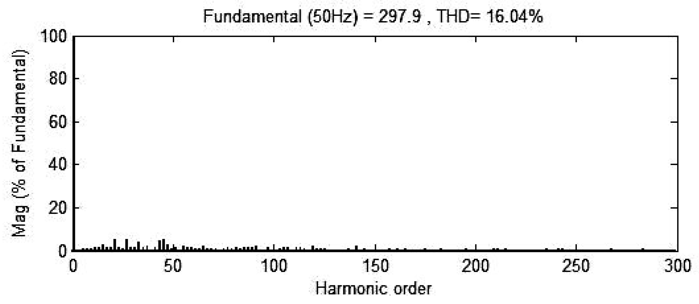
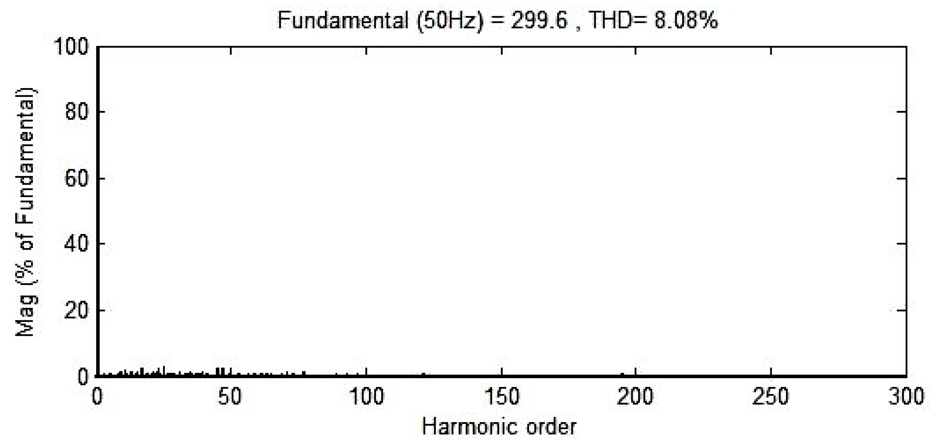
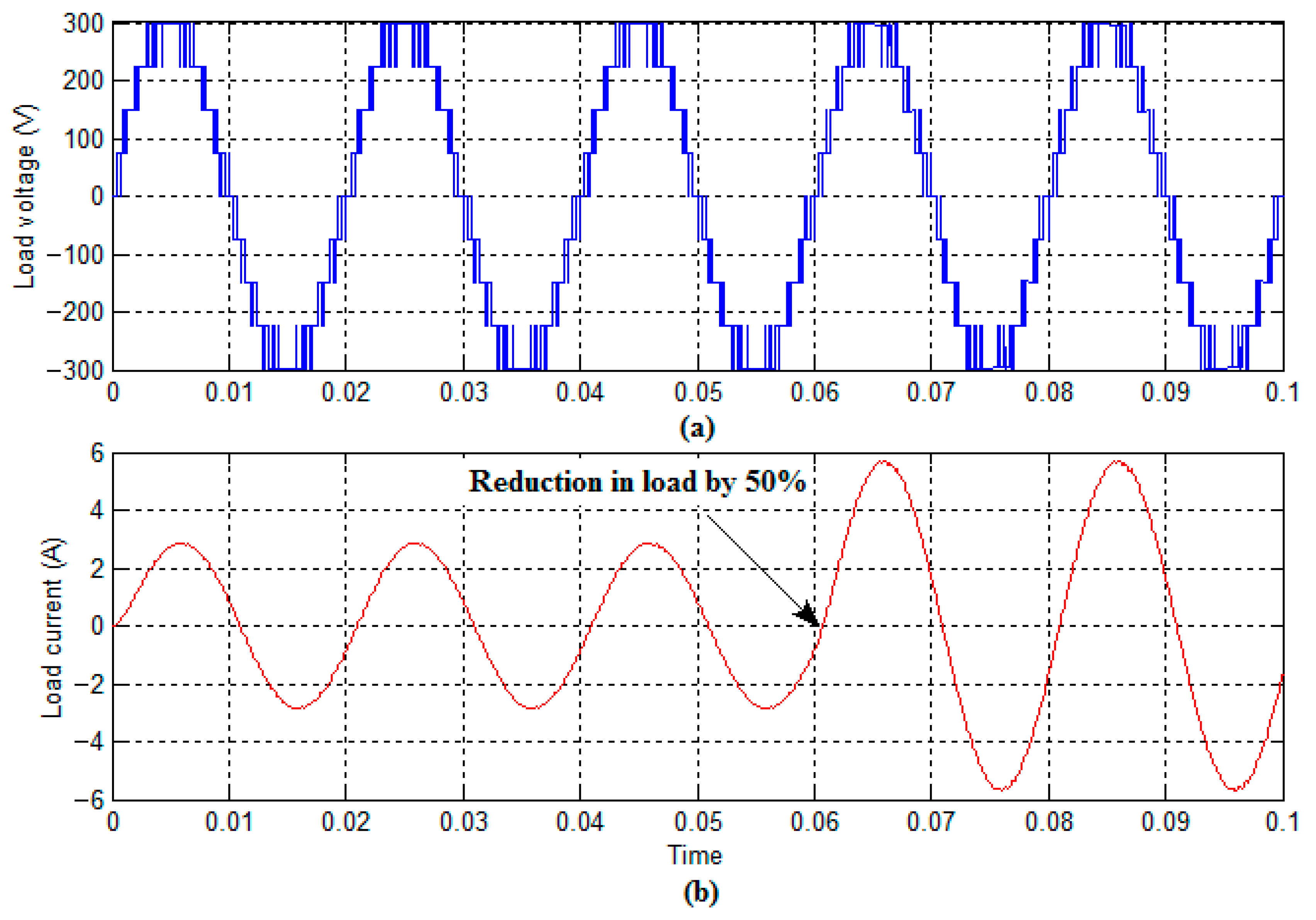
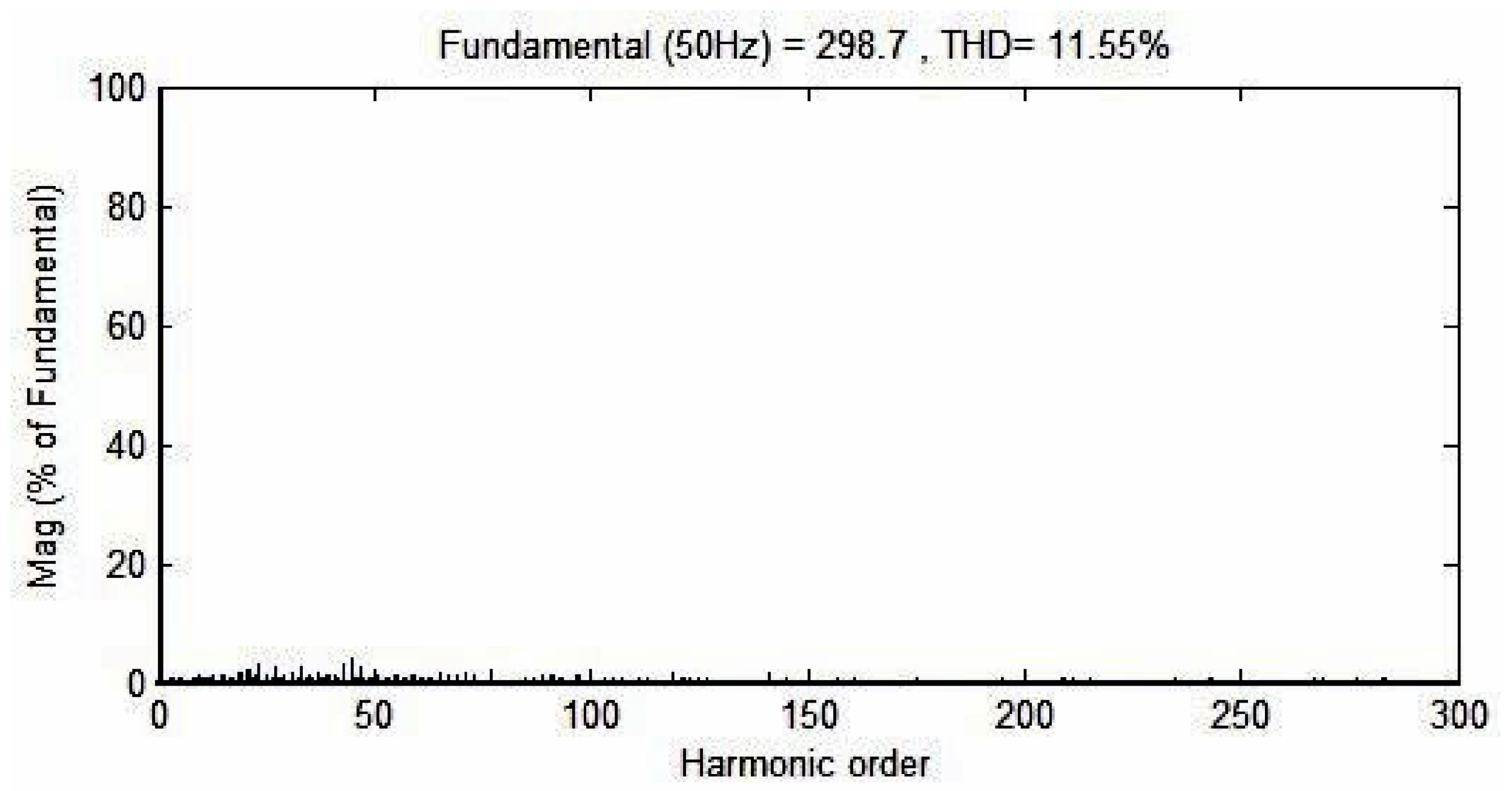
The simulations were conducted for a DC-link voltage of 100 V and a switching frequency of 2 kHz. Figure 18, Figure 19, Figure 20, Figure 21, Figure 22, Figure 23, Figure 24, Figure 25, Figure 26, Figure 27, Figure 28 and Figure 29 illustrate the simulated gating pulses, output voltage, load current, and corresponding harmonic spectra under different modulation indices (m = 0.8–1.0). The generated output voltage exhibits evenly spaced steps, confirming symmetrical voltage synthesis and balanced utilization of the DC sources. The output current waveform for the R–L load is nearly sinusoidal, verifying smooth current commutation through the bidirectional switches.
Figure 18. Simulated output voltage waveform of the proposed inverter showing 21 distinct levels. The voltage steps are evenly distributed with minimized harmonic distortion. The inset shows the corresponding switching states for one cycle.
Figure 19. Simulated output current waveform for a resistive–inductive (R–L) load. The waveform confirms smooth current transitions and continuous conduction without interruption, demonstrating the effectiveness of bidirectional switches and anti-parallel diodes.
Figure 20. Simulated output voltage spectrum of the traditional area-equalized PWM (AEPWM) method, showing dominant low-order harmonics before optimization.
Figure 21. Output voltage waveform obtained using the proposed amalgamated area-equalized fundamental-switching PWM (A2EFSPWM) technique. The waveform exhibits uniform voltage steps and reduced distortion.
Figure 22. Inductive load current response under the A2EFSPWM method. The current remains continuous and nearly sinusoidal, confirming smooth commutation and proper conduction through bidirectional switches.
Figure 23. Frequency-domain spectrum of the A2EFSPWM output voltage. The magnitudes of the 5th, 7th, 11th, and 13th harmonics are substantially reduced, resulting in improved total harmonic distortion (THD).
Figure 24. Output voltage waveform generated by the amalgamated fundamental-switching area-equalized PWM (AFSAEPWM) method, demonstrating balanced step transitions and high-quality voltage synthesis.
Figure 25. Inductive load current corresponding to the AFSAEPWM technique. The waveform closely follows a sinusoidal profile with negligible distortion, validating the harmonic suppression capability.
Figure 26. Nine-level inverter, (a) output voltage, and (b) inductive load current waveform for change in load condition.
Figure 27. Output voltage FFT spectrum for the AFSAEPWM method showing elimination of low-order harmonics and overall THD reduction below 5%.
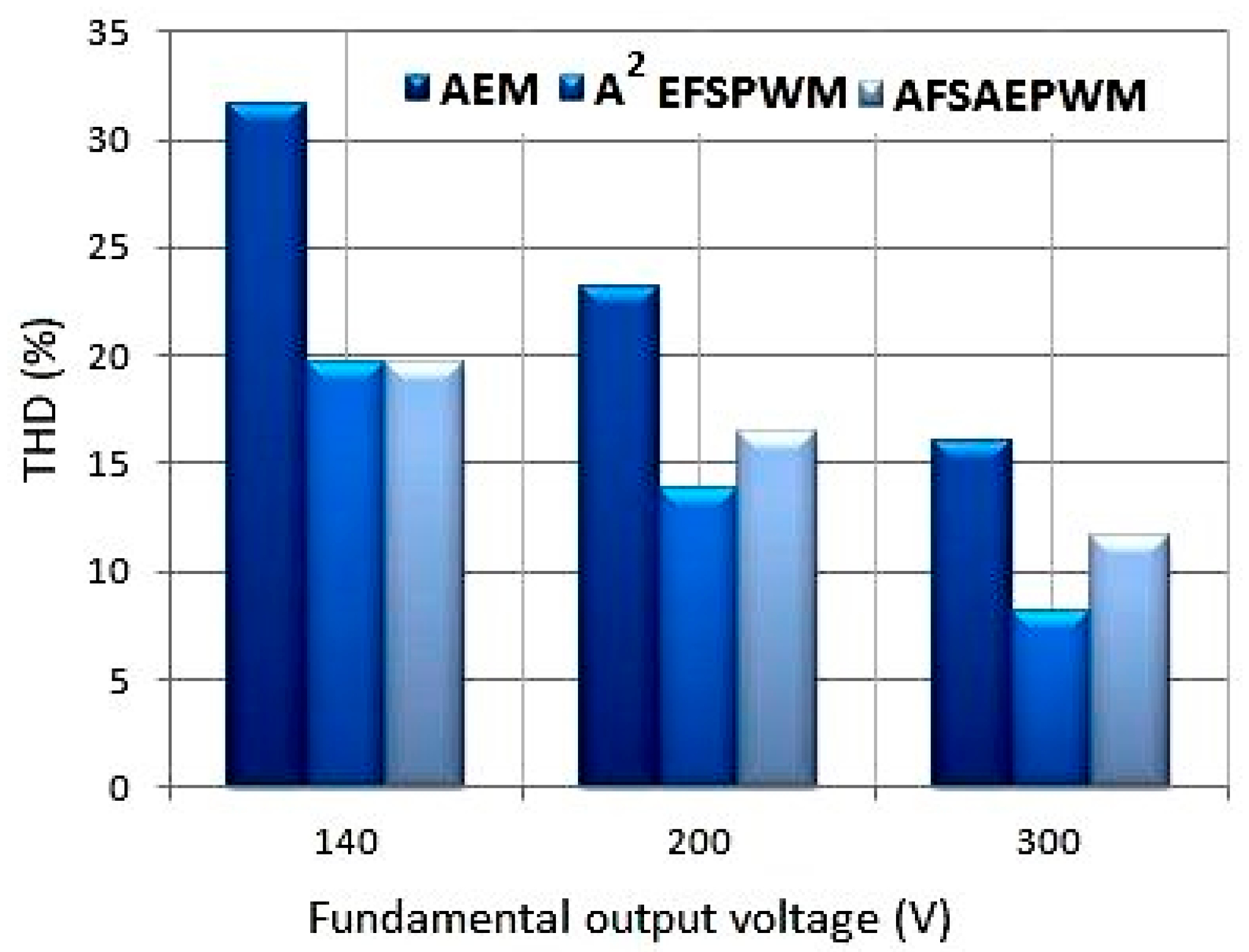
Figure 28. Comparison of the fundamental output voltage amplitude versus total harmonic distortion (THD) for different PWM strategies. The proposed hybrid PWM achieves the lowest THD at a near-unity modulation index.
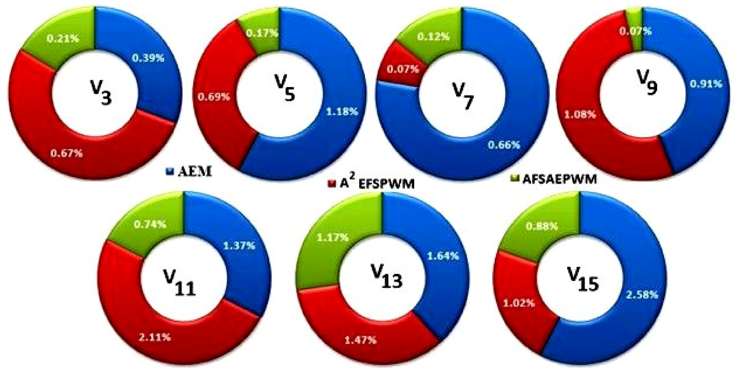
Figure 29. Variation in harmonic magnitudes between the conventional area-equalized modulation (AEM) and the proposed hybrid PWM methods. The hybrid approach exhibits significantly lower low-order harmonic content, confirming enhanced spectral performance.

6. Experimental Studies

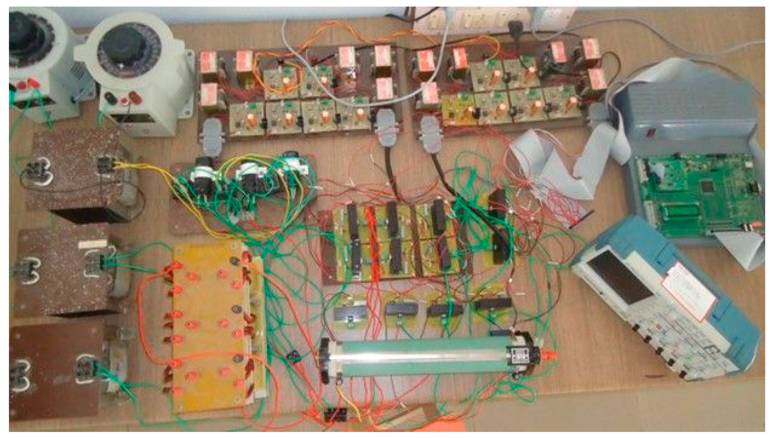
To validate the analytical and simulation outcomes, a laboratory prototype of the proposed triple-source reduced-component-count multilevel inverter (RCC-MLI) was developed and tested under controlled conditions. The experimental setup, shown in revised Figure 30, was powered by three equal DC sources rated at 33 V each, providing a total DC-link voltage of approximately 100 V. A resistive–inductive (R–L) load of 100 Ω and 100 mH was employed to emulate practical operating conditions.
Figure 30. Experimental test bench of the proposed triple-source RCC-MLI showing field-programmable gate array (FPGA) controller, gate driver circuits, IGBTs, and measurement instruments.
The gating signals were generated using a Xilinx Spartan-3E field-programmable gate array (FPGA) development board operating at a 50 MHz clock frequency. IRG4BC20SD IGBTs, driven by IR2110 gate-driver circuits, were used as the power-switching devices to ensure fast and reliable commutation.
The output voltage and current waveforms were captured using a Tektronix TDS 2024C Digital Storage Oscilloscope (with a 200 MHz bandwidth and a 2 GS/s sampling rate), while the harmonic content and efficiency were evaluated with a Fluke 43B Power Analyzer for accurate total harmonic distortion (THD) and power-quality assessment.
Revised Figure 30, Figure 31, Figure 32, Figure 33, Figure 34 and Figure 35 present the measured voltage and current waveforms for various modulation conditions. The experimental results exhibit excellent agreement with the simulation predictions, confirming precise voltage synthesis and robust harmonic suppression. The continuous current conduction through the inductive load verifies the correct operation of bidirectional switches and anti-parallel diodes during commutation (Table 3).
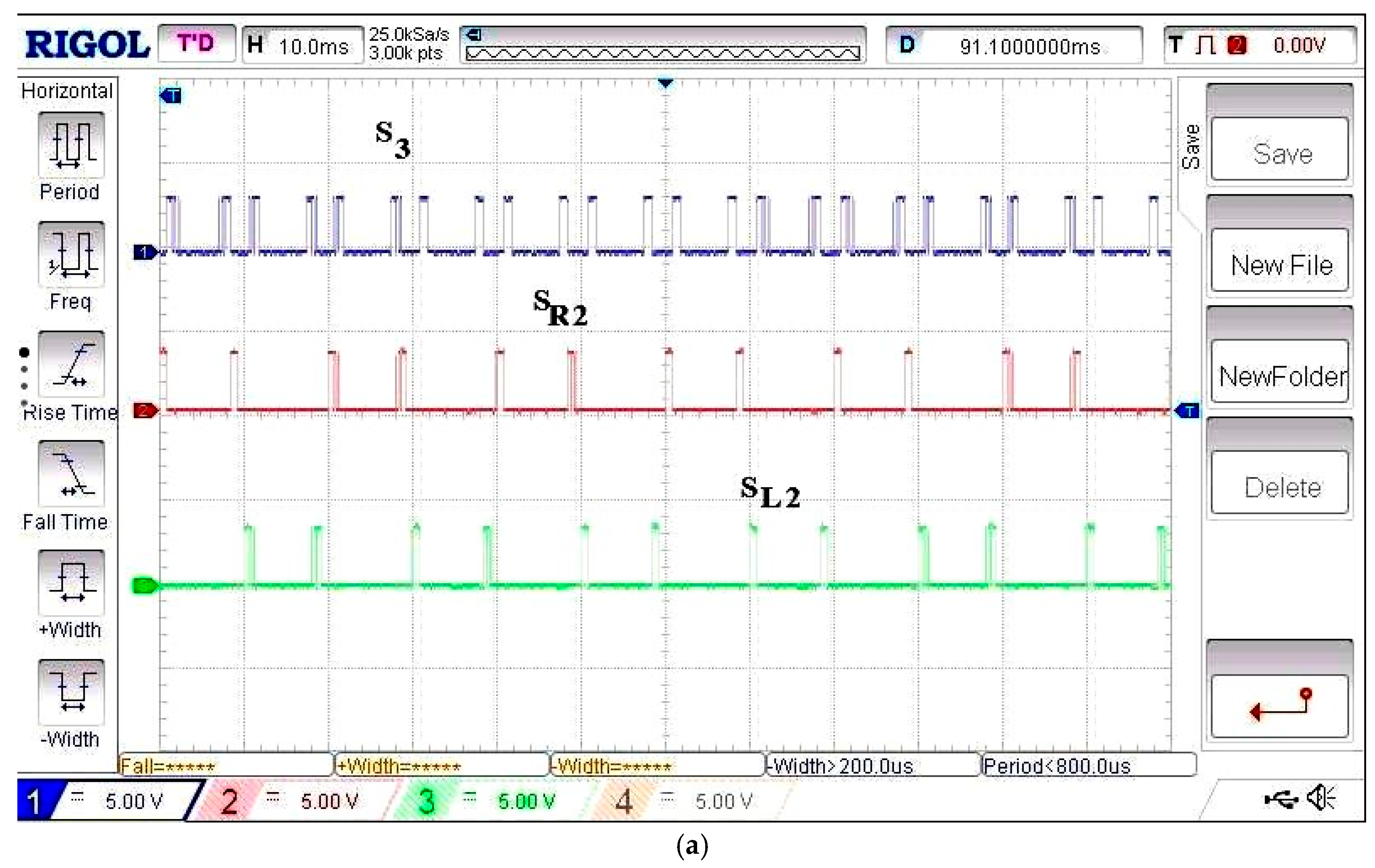
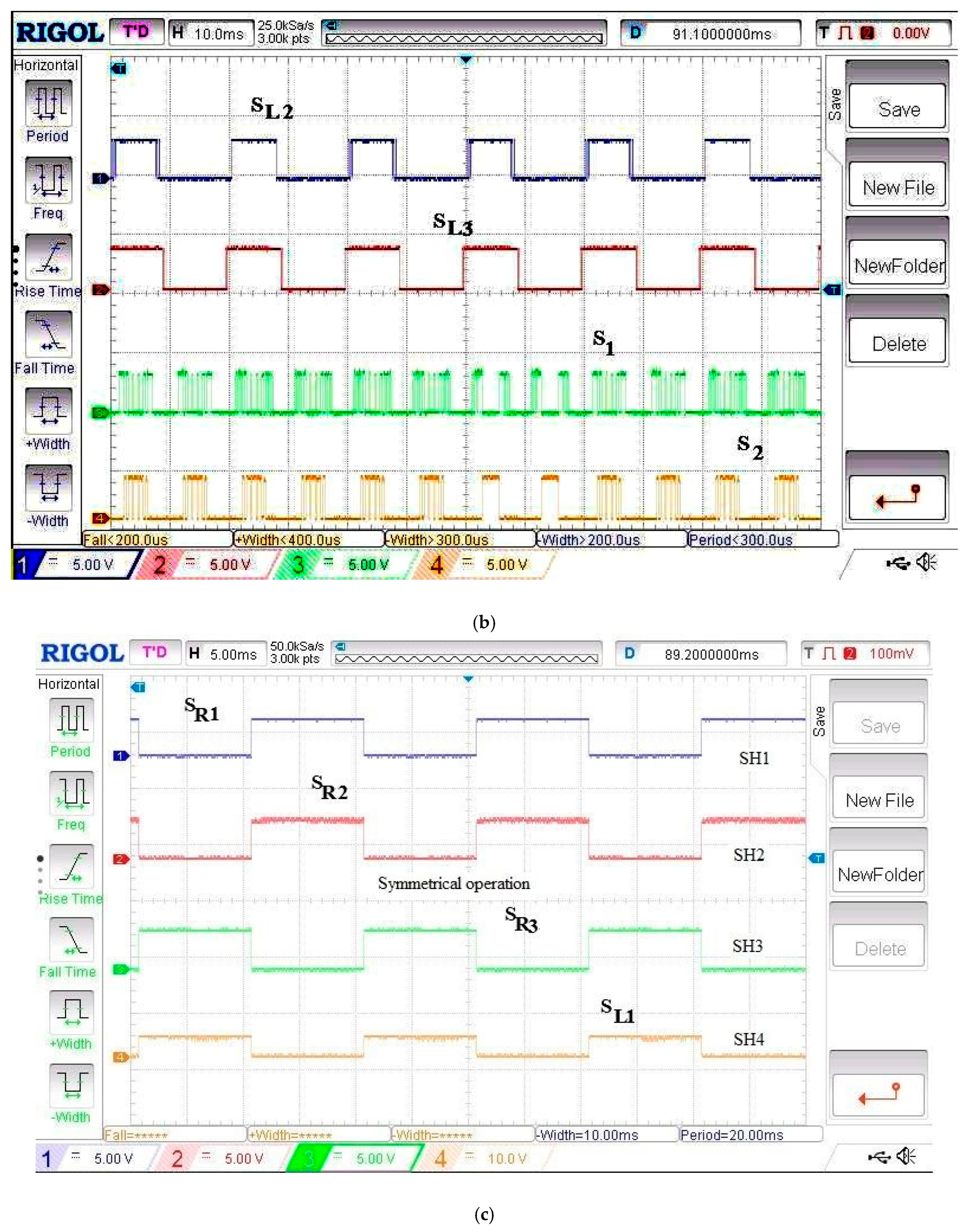
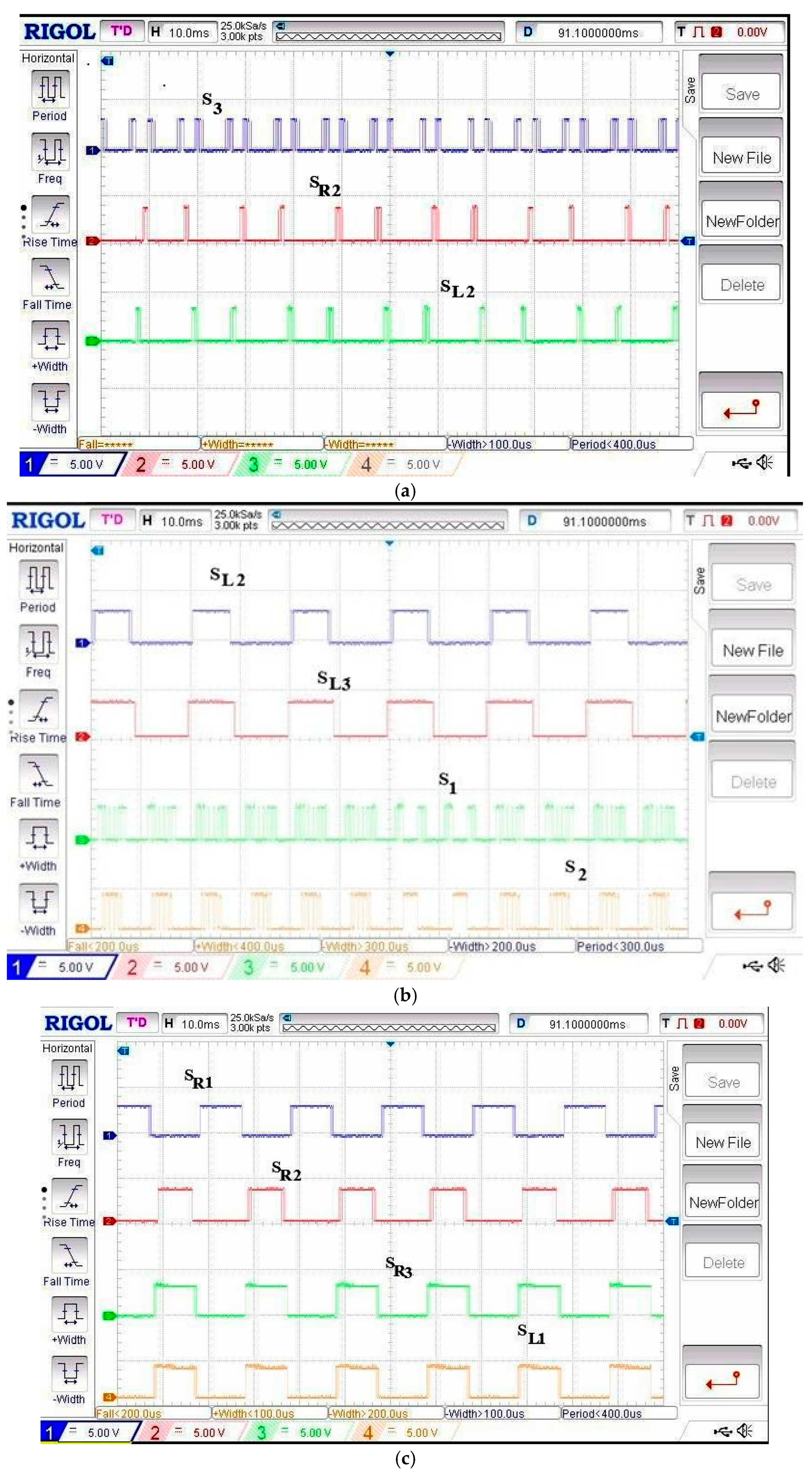
Figure 31. (a) Experimental PWM gating pattern for the A2EFSPWM method during the positive half-cycle, showing properly sequenced switching pulses generated by the FPGA controller. (b) Experimental PWM gating pattern for the A2EFSPWM method during the negative half-cycle. The symmetrical pulse arrangement confirms balanced conduction for both half-periods. (c) Composite PWM circulation pattern for the A2EFSPWM strategy combining both half-cycles, illustrating equal-area modulation and synchronized gate triggering. (ac) Experimental PWM gating patterns for the proposed amalgamated area-equalized fundamental-switching PWM (A2EFSPWM) method. Subfigures (a,b) show the positive and negative half-cycle pulse patterns, respectively, while (c) presents the composite full-cycle pulse circulation. The symmetrical pulse distribution confirms correct FPGA-based modulation and balanced conduction throughout the fundamental cycle.
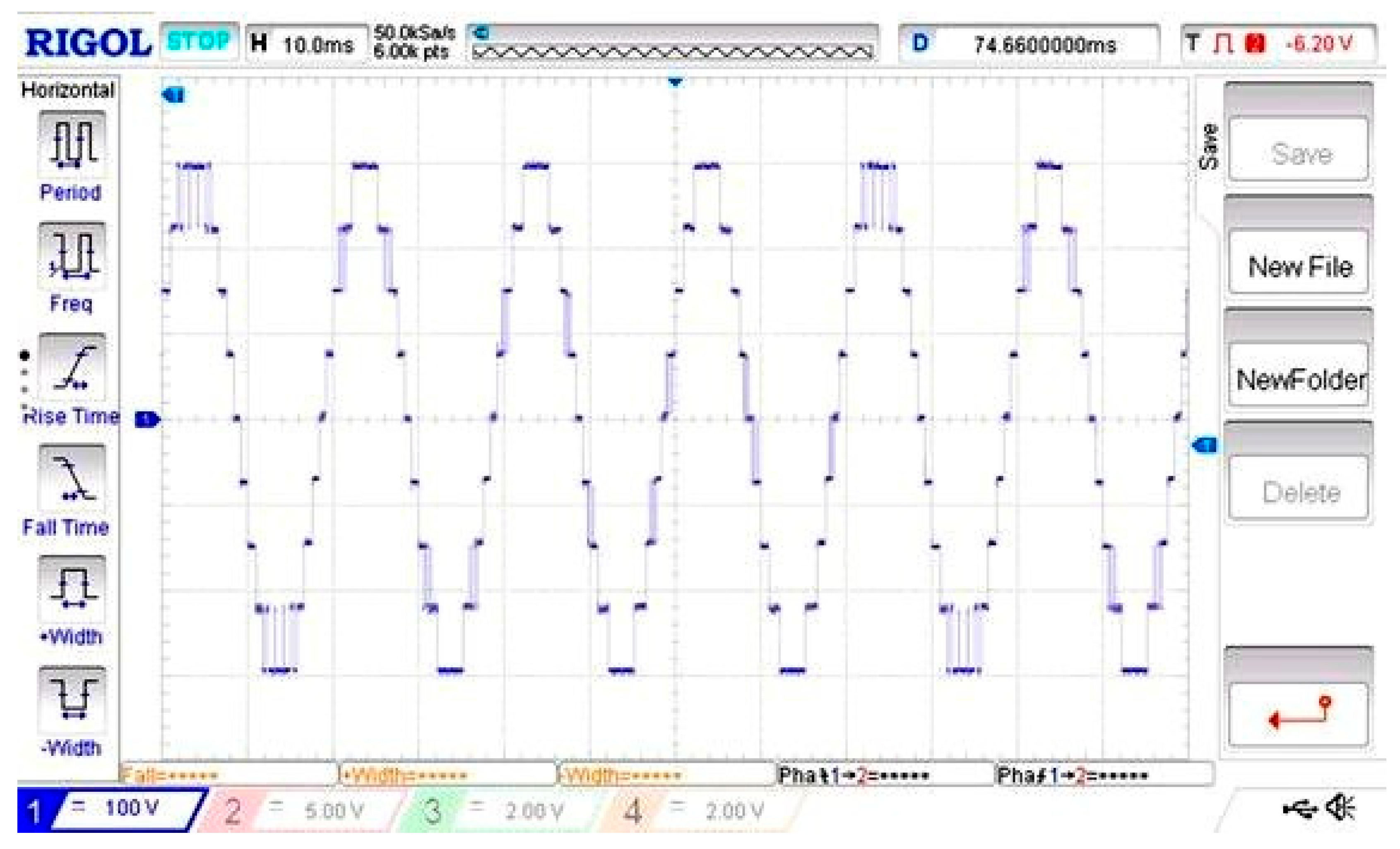
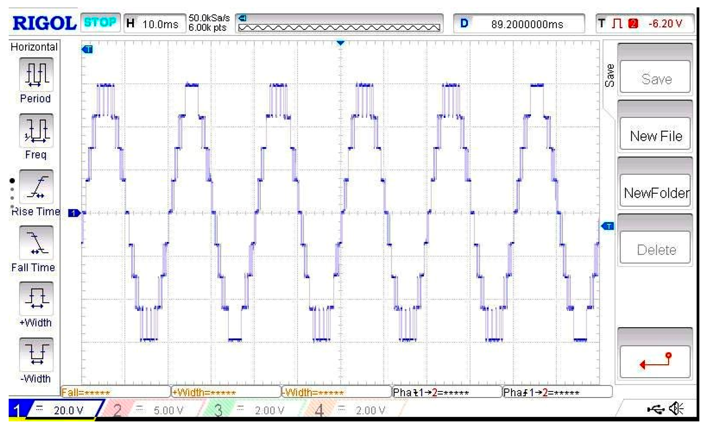
Figure 32. Experimental output voltage waveform for the A2EFSPWM method. The measured stepped waveform demonstrates accurate level synthesis and minimal distortion.
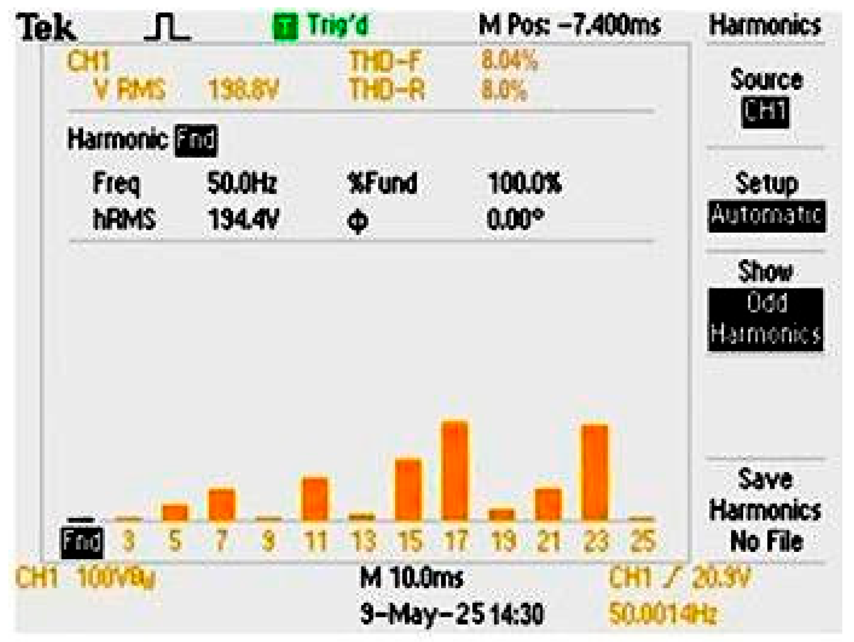
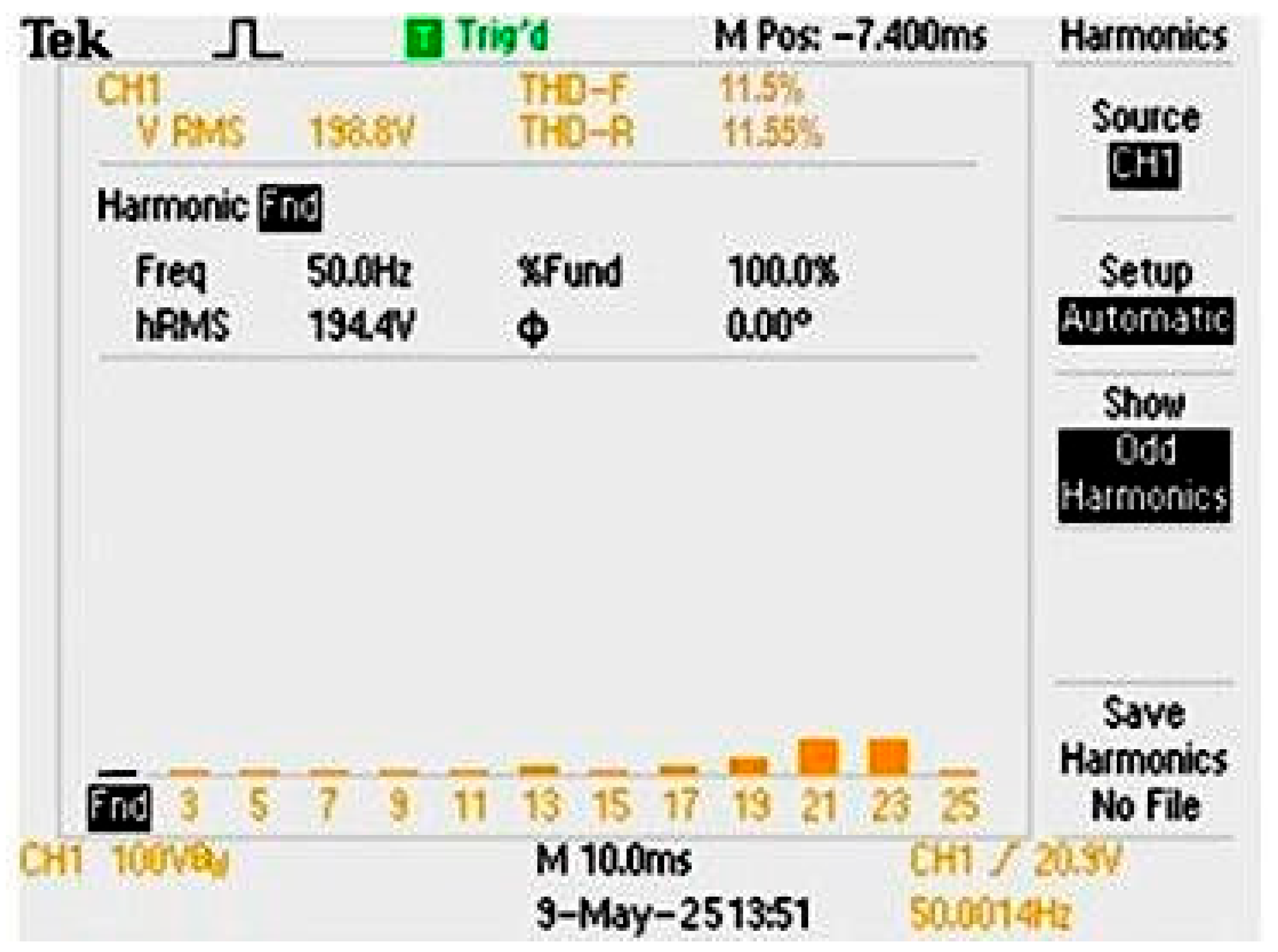
Figure 33. FFT spectrum of the experimental output voltage obtained using A2EFSPWM. The low-order harmonics (5th, 7th, 11th, and 13th) are effectively suppressed, yielding a total harmonic distortion (THD) of approximately 4.5%.
Figure 34. (a) Experimental PWM gating pattern for the AFSAEPWM technique in the positive half-cycle, generated through the hybrid carrier-less modulation approach. (b) Experimental PWM gating pattern for the AFSAEPWM method during the negative half-cycle, showing a symmetrical pulse distribution and correct timing alignment. (c) Full-cycle PWM pulse sequence for the AFSAEPWM technique, verifying synchronized operation of positive and negative intervals under equal-area control. Figure (ac) Experimental PWM gating patterns for the amalgamated fundamental-switching-area-equalized PWM (AFSAEPWM) method. Subfigures (a,b) show positive and negative half-cycle patterns, while (c) illustrates the full-cycle PWM circulation. The hybrid carrier-less modulation ensures synchronized switching and symmetry between conduction intervals.
Figure 35. Experimental output voltage waveform for the AFSAEPWM method. The stepped waveform exhibits uniform voltage intervals and high waveform fidelity.
Table 3. Simulation and experimental parameters.
Quantitatively, the measured THD of the output voltage was 4.5%, closely matching the simulated value of 4.3%, while the prototype efficiency reached 95.2%, validating the low-loss characteristics predicted analytically. The inverter operated with negligible voltage overshoot, smooth switching transitions, and stable waveform symmetry, demonstrating its effectiveness for renewable energy systems, electric vehicle drives, and medium-power industrial applications.
Minor deviations between the experimental and simulated data were attributed to switching delays, parasitic resistances, and non-idealities in the IGBTs (Table 4).
Table 4. Confirmation of excellent correlation between simulation and experimental results.
A fixed dead-time of 2 µs was implemented in the FPGA gating logic to avoid shoot-through conditions and minimize low-order harmonic distortion. The PWM generation module utilized approximately 1200 LUTs and 850 flip-flops on the Spartan-3E FPGA, operating at 50 MHz.
The experimental waveforms (Figure 31, Figure 32, Figure 33, Figure 34, Figure 35 and Figure 36) confirmed continuous current flow during switching transitions. The observed absence of current interruption validates the functionality of bidirectional switches and carrier-less modulation under inductive load conditions.
Figure 36. Measured output voltage spectrum corresponding to the AFSAEPWM technique. The spectrum reveals strong suppression of low-order harmonics, confirming enhanced power quality and reduced total harmonic distortion (THD).
The specifications of the components used in the prototype are summarized in Table 5 and filtering elements employed in the prototype are presented in Table 2. These selections ensure proper voltage and current ratings, reliable switching, and stable operation under the rated load conditions.
Table 5. The detailed specifications of the power semiconductor devices, gate driver units, controller, and filtering elements employed in the prototype are presented below.
A comparative evaluation of the proposed triple-source reduced-component MLI against recently reported topologies is presented in Table 6.
Table 6. A comparative evaluation of the proposed triple-source reduced-component MLI against recent topologies reported in [,,,,,,,].
The proposed configuration achieves a 45% reduction in switching devices and gate drivers compared with existing reduced-component-count multilevel inverters (RCC MLIs), while maintaining lower voltage stress (≈45% Vdc) and achieving the lowest THD (4.3%). Owing to the carrier-less hybrid PWM control and minimized conduction paths, the overall inverter efficiency improves to 95.2%. These results confirm the superiority of the proposed system in terms of component economy, harmonic performance, and conversion efficiency (Table 7).
Table 7. Comparative performance analysis of PWM strategies.

7. Conclusions

This paper presented a novel triple-source reduced-component-count multilevel inverter (RCC-MLI) integrated with a carrier-less hybrid pulse-width modulation (PWM) strategy for enhanced power conversion performance. The proposed cross-connected configuration substantially minimizes the number of semiconductor switches and gate drivers required for a given output voltage level. Only four switches conduct at any instant, achieving approximately a 33% reduction in semiconductor devices compared with conventional MLIs of similar voltage ratings.
Comprehensive analytical modeling, MATLAB/Simulink simulations, and experimental validation on a nine-level prototype confirmed the feasibility and accuracy of the design. The proposed hybrid PWM algorithm based on the equal-area criterion eliminates the need for carrier and reference waveforms, simplifying real-time digital implementation while maintaining smooth and symmetric voltage generation. The inverter also achieves a higher effective switching frequency without increasing individual device commutations, thus improving waveform linearity and reducing harmonic distortion.
Quantitative analysis shows that the proposed topology achieves a total harmonic distortion (THD) reduction from 8.2% to 4.3% and an efficiency improvement from 91.5% to 95.2%, compared with conventional multicarrier PWM-based MLIs. The blocking voltage across each device is limited to approximately 45% of the total DC-link voltage, reducing device stress and enhancing long-term reliability. Experimental waveforms closely match analytical and simulated predictions, confirming excellent harmonic suppression, continuous current conduction under inductive loading, and an improved dynamic response.
The reduced component count, simplified gating structure, minimized switching losses, and FPGA-based real-time control make the proposed inverter highly suitable for renewable-energy interfaces, medium-power industrial drives, and electric vehicle powertrains.
Future research will focus on extending the proposed topology to three-phase configurations, higher voltage and power levels, and grid-connected applications. Additionally, advanced adaptive and bidirectional PWM control techniques will be explored to optimize harmonic performance and efficiency under varying source and load conditions. These developments are expected to further enhance the inverter’s potential for deployment in next-generation clean-energy systems and smart electric drive applications.

Author Contributions

Conceptualization, R.S. and K.C.; methodology, R.S.; software, R.S.; validation, K.C. and R.S.; formal analysis, K.C.; investigation, R.S.; resources, R.S.; data curation, R.S.; writing—original draft preparation, R.S.; writing—review and editing, K.C.; visualization, K.C.; supervision, K.C.; project administration, K.C.; funding acquisition, K.C. All authors have read and agreed to the published version of the manuscript.

Funding

This research received no external funding.

Data Availability Statement

The original contributions presented in this study are included in the article. Further inquiries can be directed to the corresponding author.

Conflicts of Interest

The authors declare no conflicts of interest.

References

  1. Pragathi, B.; Kumar, S.; Kumari, P.R.; Singh, A.R. Performance Evaluation of Hybrid Multistage Inverter with a High-Frequency Switching Technique. J. Eng. Appl. Sci. 2023, 70, 101. [Google Scholar] [CrossRef]
  2. Farsijani, M.; Abbasian, S.; Hafezi, H. A Novel Hybrid Single-Phase Modular Multistage Inverter Algorithm with Enhanced Stages per Device Count. In Proceedings of the IEEE International Conference on Environment and Electrical Engineering and Industrial and Commercial Power Systems Europe (EEEIC & CPS Europe), Madrid, Spain, 6–9 June 2023; IEEE: New York, NY, USA, 2023. [Google Scholar] [CrossRef]
  3. Ramaprabha, R. A Single-Phase Multistage Inverter with Cascaded Basic Units. In Proceedings of the IEEE Green Connected Automation Technologies (GCAT), Bengaluru, India, 7–9 October 2022; IEEE: New York, NY, USA, 2022. [Google Scholar] [CrossRef]
  4. Karakılıç, M.; Almalı, M.N. Design of Hybrid Switched Diode Multistage Inverter Using Individual DC Source. J. Electr. Eng. Technol. 2024, 19, 4169–4180. [Google Scholar] [CrossRef]
  5. Augustin, A.; Annamalai, T.; Karthikeyan, R. PV Based Modified Cascaded Inverter for Drives Application. In Proceedings of the 9th International Conference on Electrical Energy Systems (ICEES), Chennai, India, 23–25 March 2023; IEEE: New York, NY, USA, 2023; pp. 461–466. [Google Scholar] [CrossRef]
  6. Leedy, A.W.; Aganah, K.A.; Abdel Raziq, M.; Booth, K. A Single Phase Five Level Inverter Algorithm for Distributed Sources. In Proceedings of the 2nd IEEE Industrial Electronics Society Annual Online Conference (ONCON), Virtual, 8–10 December 2023; IEEE: New York, NY, USA, 2023; pp. 336–341. [Google Scholar] [CrossRef]
  7. Baksi, S.K.; Behera, R.K.; Al Jaafari, K.; Al Hosani, K.; Muduli, U.R. Seventeen Level Switch Capacitor-Based Cascaded Multilevel Inverter. In Proceedings of the IECON 2023—49th Annual Conference of the IEEE Industrial Electronics Society, Singapore, 16–19 October 2023. [Google Scholar]
  8. Winil, C.W.; Aishwarya, V. Comparative Study of Minimized Switch Multistage Inverter Topologies. In Intelligent Solutions for Smart Grids and Smart Cities: IPECS 2022; Siano, P., Williamson, S., Beevi, S., Eds.; Springer: Singapore, 2023; pp. 461–477. [Google Scholar] [CrossRef]
  9. Stonier, A.A.; Yazhini, M. Implementation of Multistage Inverter with Minimized Switching Components. In Recent Advances in Power Electronics and Drives, Lecture Notes in Electrical Engineering; Springer: Singapore, 2023; Volume 1022, pp. 137–153. [Google Scholar] [CrossRef]
  10. Sathi, G.K.; Kumar, C.S. Design of Microcontroller Based Multistage Inverter. IOSR J. Electr. Electron. Eng. 2014, 9, 81–84. [Google Scholar] [CrossRef]
  11. Behera, B.; Padhee, G.; Mohapatra, S. Seven Level Cascaded H-Bridge Multistage Single-Phase Inverter Implemented with an ATMEGA Microprocessor. In Proceedings of the 49th IEEE Photovoltaic Specialists Conference (PVSC), Philadelphia, PA, USA, 5–10 June 2022; IEEE: New York, NY, USA, 2022. [Google Scholar] [CrossRef]
  12. Kubendran, V.; Shuaib, Y.M.; Roselyn, J.P. Development of Multistage Inverter with Minimized Switch Counts and Limited Sources for Electric Vehicles. Sustain. Energy Technol. Assess. 2022, 52, 102332. [Google Scholar] [CrossRef]
  13. Amir, M.; Alam, M.S.; Haque, A.; Bakhsh, F.I.; Shah, N. Design and Implementation of a Minimized Switch Seventeen-Level Multistage Inverter for Grid Integration of Battery Storage System. J. Energy Storage 2024, 86, 101234. [Google Scholar] [CrossRef]
  14. Salman, M.; Haq, I.U.; Ahmad, T.; Ali, H.; Qamar, A.; Basit, A.; Khan, M.; Iqbal, J. Minimization of Overall Harmonic Distortions of Cascaded H-Bridge Multistage Inverter by Utilizing Bio-Inspired AI Algorithm. EURASIP J. Wirel. Commun. Netw. 2020, 2020, 66. [Google Scholar] [CrossRef]
  15. Shanono, I.H.; Abdullah, N.R.H.; Muhammad, A. A Three-Phase Five-Level Multistage Inverter Using a Single DC Source and Modified Cascaded H-Bridge Algorithm. Indones. J. Electr. Eng. Comput. Sci. 2018, 12, 924–932. [Google Scholar] [CrossRef]
  16. Shanono, I.H.; Abdullah, N.R.H.; Daniyal, H.; Muhammad, A. Selective Harmonic Elimination (SHE)-Based 3-Phase Multilevel VSI for Standalone Applications. SN Appl. Sci. 2019, 1, 1512. [Google Scholar] [CrossRef]
  17. Jayabalan, M.; Jeevarathinam, B.; Sandirasegarane, T. Minimized Switch-Count Pulse-Width-Modulated Multistage Inverter. IET Power Electron. 2017, 10, 10–17. [Google Scholar] [CrossRef]
  18. Taheri, A.; Samsami, H. New Algorithm of a Switched-Capacitor-Based Multistage Inverter with a Single DC Power Supply. IET Power Electron. 2019, 12, 1571–1584. [Google Scholar] [CrossRef]
  19. Anand, V.; Singh, V. Compact Symmetrical and Asymmetrical Multistage Inverter with Minimized Switches. Int. Trans. Electr. Energy Syst. 2020, 30, e12458. [Google Scholar] [CrossRef]
  20. Khosroshahi, M.T. Crisscross Cascade Multistage Inverter with Reduction in Component Count. IET Power Electron. 2014, 7, 2914–2924. [Google Scholar] [CrossRef]
  21. Jose, S.E.; Titus, S. A Level Dependent Source Concoction Multistage Inverter Algorithm with a Minimized Count of Power Switches. J. Power Electron. 2016, 16, 1316–1323. [Google Scholar] [CrossRef]
  22. Gupta, K.K.; Jain, S. A Novel Multistage Inverter Based on Switched DC Sources. IEEE Trans. Ind. Electron. 2014, 61, 3269–3278. [Google Scholar] [CrossRef]
  23. Majumdar, S.; Mahato, B.; Jana, K.C. Optimum Structure-Based Multilevel Inverter with Doubling Circuit Configuration. J. Circuits Syst. Comput. 2019, 28, 1950194. [Google Scholar] [CrossRef]
  24. Hinago, Y.; Koizumi, H. A Single-Phase Multistage Inverter Using Switched Series/Parallel DC Voltage Sources. IEEE Trans. Ind. Electron. 2010, 57, 2643–2650. [Google Scholar] [CrossRef]
  25. Banaei, M.R.; Salary, E. Asymmetric Cascaded Multilevel Inverter: A Solution to Obtain High Voltage Levels. J. Electr. Eng. Technol. 2013, 8, 316–325. [Google Scholar] [CrossRef]
  26. Thamizharasan, S.; Sudha, L.U.; Baskaran, J.; Ramkumar, S.; Jeevananthan, S. Carrier-Less Pulse Width Modulation Strategy for Multistage Inverters. IET Power Electron. 2015, 8, 1601–1609. [Google Scholar] [CrossRef]
Disclaimer/Publisher’s Note: The statements, opinions and data contained in all publications are solely those of the individual author(s) and contributor(s) and not of MDPI and/or the editor(s). MDPI and/or the editor(s) disclaim responsibility for any injury to people or property resulting from any ideas, methods, instructions or products referred to in the content.

Article Metrics

Citations

Article Access Statistics

Article metric data becomes available approximately 24 hours after publication online.