Article

A New Asymmetric H-6 Structured Multilevel Inverter with Reduced Power Components

by
Annadurai Radhakrishnan
1,*,
Elankurisil S. Arasan
2,
Balamurugan C. Ramalingam
3 and
Kannan Chandrasekaran
4
1
Department of Electrical and Electronics Engineering, Research Scholar, Anna University, Chennai 600 025, India
2
Department of Electrical and Electronics Engineering, Adhiparasakthi Engineering College, Melmaruvathur 603 319, India
3
Department of Electrical and Electronics Engineering, Er Perumal Manimegalai College of Engineering, Hosur 635 117, India
4
Department of Electrical and Electronics Engineering, Arunai Engineering College, Tiruvannamalai 606 603, India
*
Author to whom correspondence should be addressed.
Symmetry 2024, 16(1), 72; https://doi.org/10.3390/sym16010072
Submission received: 7 December 2023 / Revised: 29 December 2023 / Accepted: 3 January 2024 / Published: 5 January 2024
(This article belongs to the Section Engineering and Materials)

Abstract

:
Multilevel inverters play a key role in improving the power quality for industrial, domestic, and renewable energy sectors due to sinusoidal output voltage through small voltage steps, lesser THD (total harmonic distortion), and EMI (electromagnetic interference). There are several variants in MLI structures to generate a stepped voltage with their own operating characteristics, which flaws in switching devices with gate drivers, current conducting switches varied with varied voltage levels, and switches with different abilities in blocking voltagesto overcome increases in implementation costs and restrict its usage in high-power applications. Therefore, this article paves a solution for the above problem, which orients a new structure for asymmetric operation to propel large voltage levels with small values of switches in parallel with conventional topologies. The subtlety of the proposed topology is governed by a multicarrier pulse width modulation scheme, and ten different voltage magnitude algorithms are developed and compared foreffectiveness.Hitherto, many existing MLI topologies with reduced power switches have beendeveloped; among these, the H6 structure attempts to curtail the reduced conduction path. The operation of the suggested topology is confirmed in a Matlab/Simulink environment, and real-time performance is investigated using a laboratory prototype to accord the simulated results.

1. Introduction

The multilevel inverter (MLI) is an alternative solution for three-leg inverters in industrial and utility applications owing to several merits like high-quality output voltage, lower THD, lesser dv/dt, and lower EMI [1,2,3]. In multilevel inverters, the output quality is enriched by raising the number of steps in the load voltage waveform. This increases the number of DCpower sources, DC-link capacitors, and power switches, which increases the cost and accrues diligent control methods. Several remarkable topologies playa significant role in industrial adjustable speed drives and renewable energy applications [4,5,6]. The cascaded H-bridge inverters find extensive use in industrial drivers due to their modular structure, fault-tolerant recovery capability, and exemption from capacitor voltage balancing issues. However, they require a higher count of input DC power supplies and switching devices with voltage steps [7]. A new topology using a single DC source for a grid-connected PV system is introduced to achieve higher voltage levels using the level doubling concept. The developed system is composed of a single DC source-fed full bridge inverter and capacitor-fed half bridge leg to complete the entire system for grid interface applications [8]. A new 49-level inverter is developed using two packed U-cell structures sharing a common DC source through a high-frequency link. This topology needs a small number of switches, and a typical design is required for a high-frequency link transformer [9]. A pair of DC sources and capacitors with several switches form a 9-level inverter, and the topology looks simple in its state of operation. However, capacitor voltage balancing is not portrayed to obtain balanced voltage levels [10]. A topology using six unidirectional switches and one bidirectional switch to generate 7- and 11-level output voltages, respectively, is formulated for renewable energy applications. This topology is extended to produce more voltage levels in cascaded connections [11]. A new hybrid cascaded topology for medium and high voltage applications is introduced using six switches, three identical DClinks, and two blocking voltages. This topology produces six positive voltage states and negative voltage states are acquired through an H-bridge inverter [12]. A modified MLI topology for an asymmetrical structure using ten switches and four DC sources is used to achieve 21-level output on the inverter output side. This topology claims it is modular and impacts high power quality [13]. A new asymmetrical voltage source input topology is constructed using four DC sources and nine switches to obtain seventeen voltage levels. The topology with a cascaded structure produces voltage levels with less stress on the switches used in the proposed structure [14]. A topology with three different voltage sources and ten switches to generate a 15-level voltage for renewable and industrial applications is presented to offer a new structure in reduced count topologies [15]. A couple of DC sources and a capacitor areused to form a new MLI to generate a stepped output voltage. The topology uses fewerswitches and DC sources to offer higher voltage levels [16]. A module consists of a single DC source and a capacitor connected through seven switches to generate voltage levels. The structure can be extended with different voltage values in the voltage source to cascade with the basic symmetrical structure with the same number of switches doubled while cascading to achieve higher voltage levels. The topology requires suitable control for balancing the capacitor voltages [17]. A switched capacitor MLI is developed to overcome the drawbacks of the traditional cascaded H-bridge inverter with the use of a single DC source and DC capacitors. However, the topology suffers from a sudden rush in current in switched capacitors, and this problem is alleviated through charging inductors [18]. A switched DC source MLI is conceived using three DC sources and five switches. The topology generates all possible voltage levels with a series of a half-bridge cell and an H-bridge inverter. The topology requires high blocking voltage switches in the H-bridge inverter, and the value rises with an increase in voltage levels [19]. A switched inductor Z-source network is incorporated with the traditional MLI to exploit the properties of less THD and low electromagnetic interference [20]. A CHBMLI using a single DC source and a reduced number of transformers for active filter applications is developed to enjoy the merits of elimination of harmonics during nonlinear loads. However, the objective of diminishing the cost of switches and DC sources in developed topology increases the size of coupling transformers [21]. A CHBMLI is connected in a three-phase configuration that employs a single DC source and floating capacitors per phase. The floating capacitors serve the purpose of a level-doubling network without the use of a closed-loop control. The capacitor voltage of each H-bridge is equal to half; the voltage of the preceding H-bridge claiming binary asymmetric ratio is another advantage [22]. The arrangement of DC sources and capacitors in ‘E’ and ‘F’ shapesoffers reduced power components in the MLI structure, ‘E’ module helpsthe capacitor voltage divider to double the voltage levels. The capacitor voltages are balanced without complex control methods [23]. A dual DC source and a series of capacitors with several switches to fetch the stepped DC voltage and an H-bridge inverter areused to attain all voltage levels. The structure is nonmodular and a capacitor voltage balancing method is required [24]. A switched capacitor-based MLI structure usesa single DC source and fewer switches, diodes, and capacitors to claim a reduced power component in the MLI family. The DC capacitors are charged in a trinary ratio to result in a DC-boosted voltage [25]. A novel structure using three DC sources and eight switches to generate a stepped DC voltage and an H-bridge inverter is used to attain a stepped AC voltage level. The topology uses several modules to enrich the voltage levels [26]. A new MLI based on several subcellsis made from two DC sources and six switches, and it produces a 125-level asymmetrical configuration. The MLI uses less subcells to emulate CHBMLI with asymmetric voltage sources for enhancing the output voltage levels [27]. A new MLI using four DC sources is arranged in a hut-shaped structure to accumulate a 15-level stepped voltage. The topology uses only three DC sources in their modes of operation and one DC source falls under an unused state [28]. An H-bridge type module is made up of three DC sources and several switches to achieve stepped voltage. The topology is cascaded with several modules to improve voltage levels and reduce stress on the switches [29]. A transistor-clamped double DC source with an H-bridge is developed for solar energy applications and the topology appears similar to traditional transistor-clamped topologies [30].
In this context, a new topology is generalized to achieve possible voltage levels using reduced switches with less blocking voltage. The topology is developed to configure asymmetrical voltage sources to reach maximum voltage levels. There are nine different voltage methods that have been introduced to check the viability of the developed topology in asymmetrical configurations.
This paper is organized as follows: In Section 1, the focus is on exploring recent advancements in multilevel inverters. Section 2 demonstrates the planned proposed asymmetric H-6 topology and different operating modes. Section 3 involves delving into simulations and experimental investigations, engaging in a thorough comparative study that encompasses an analysis of other referenced topologies. Section 4 describes theconclusion and possible application.

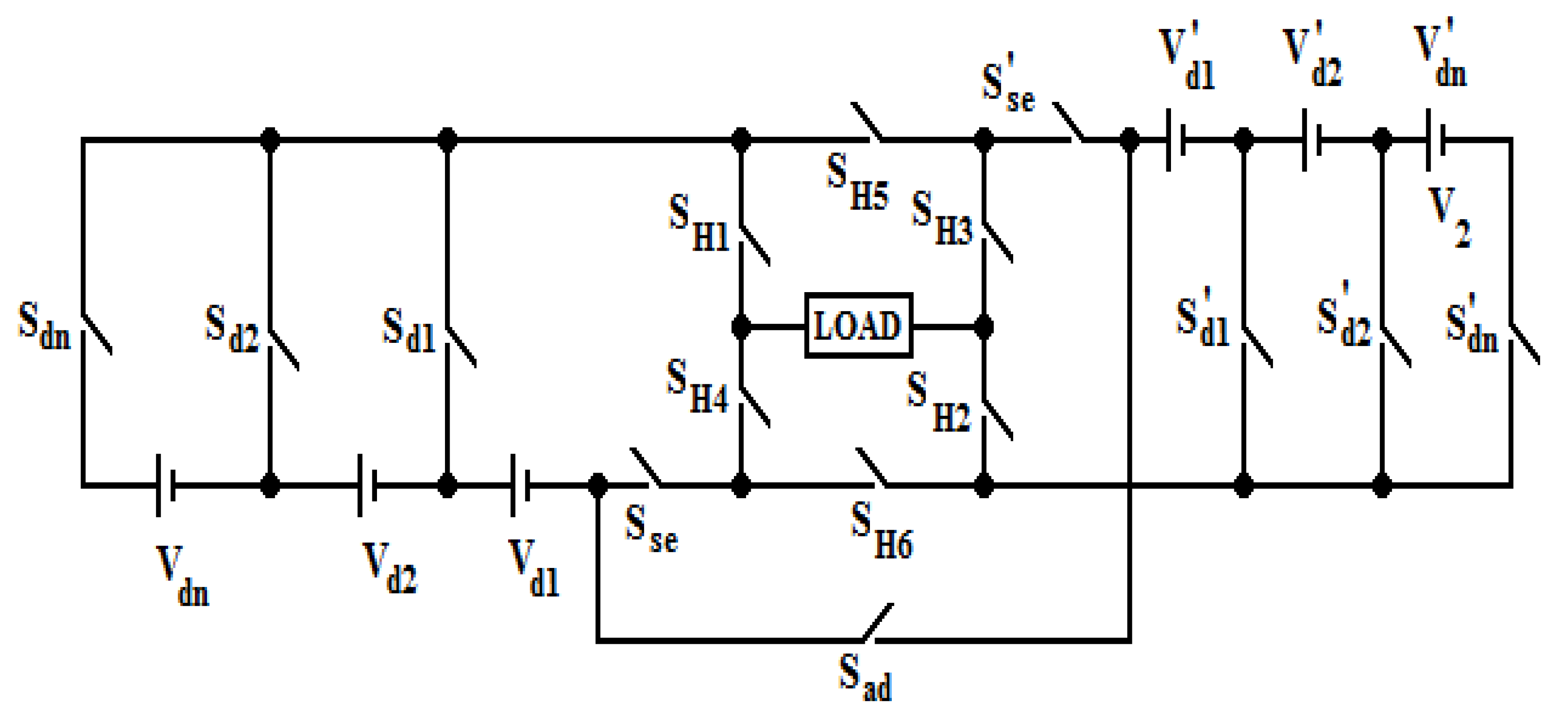
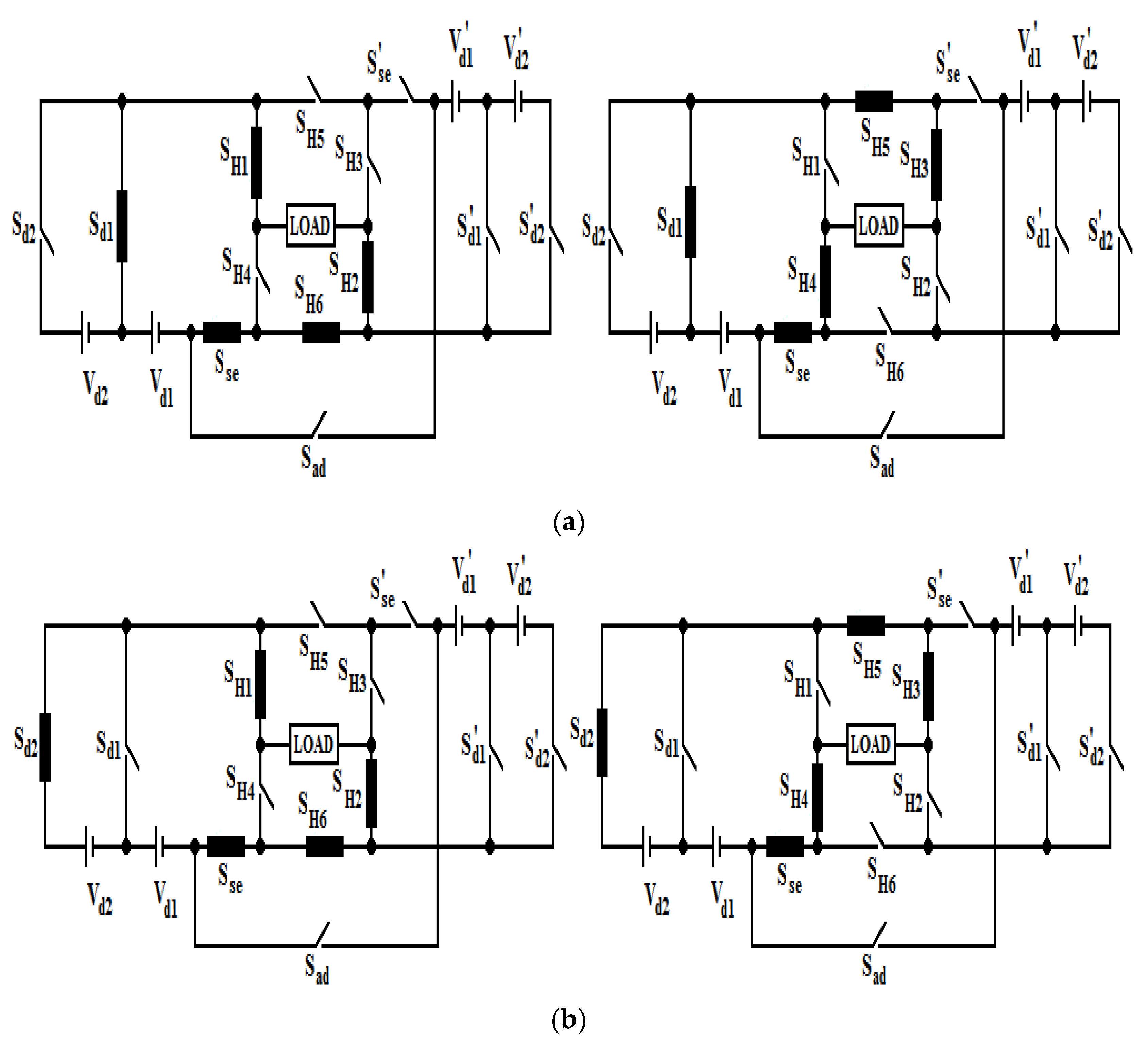
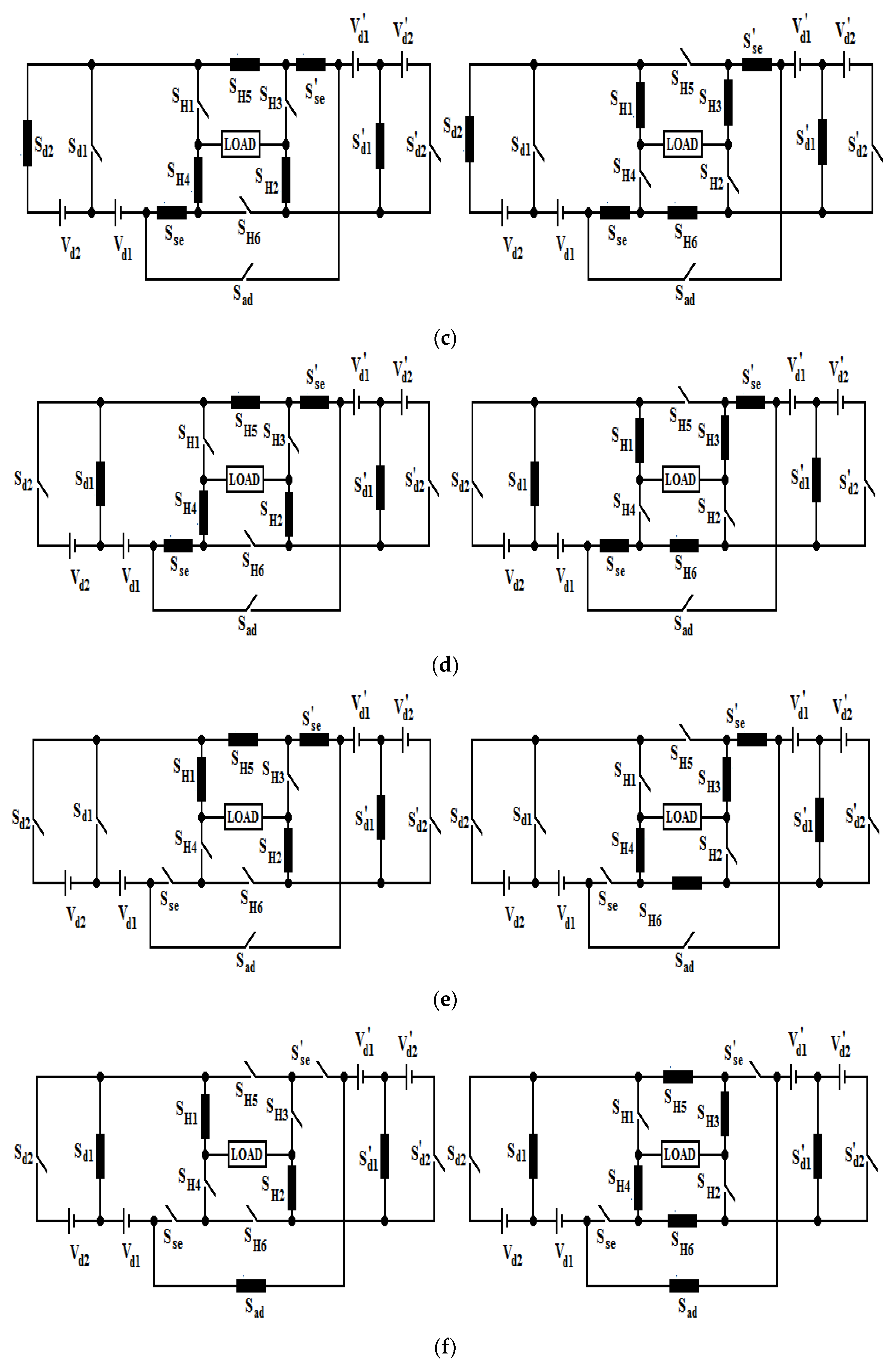
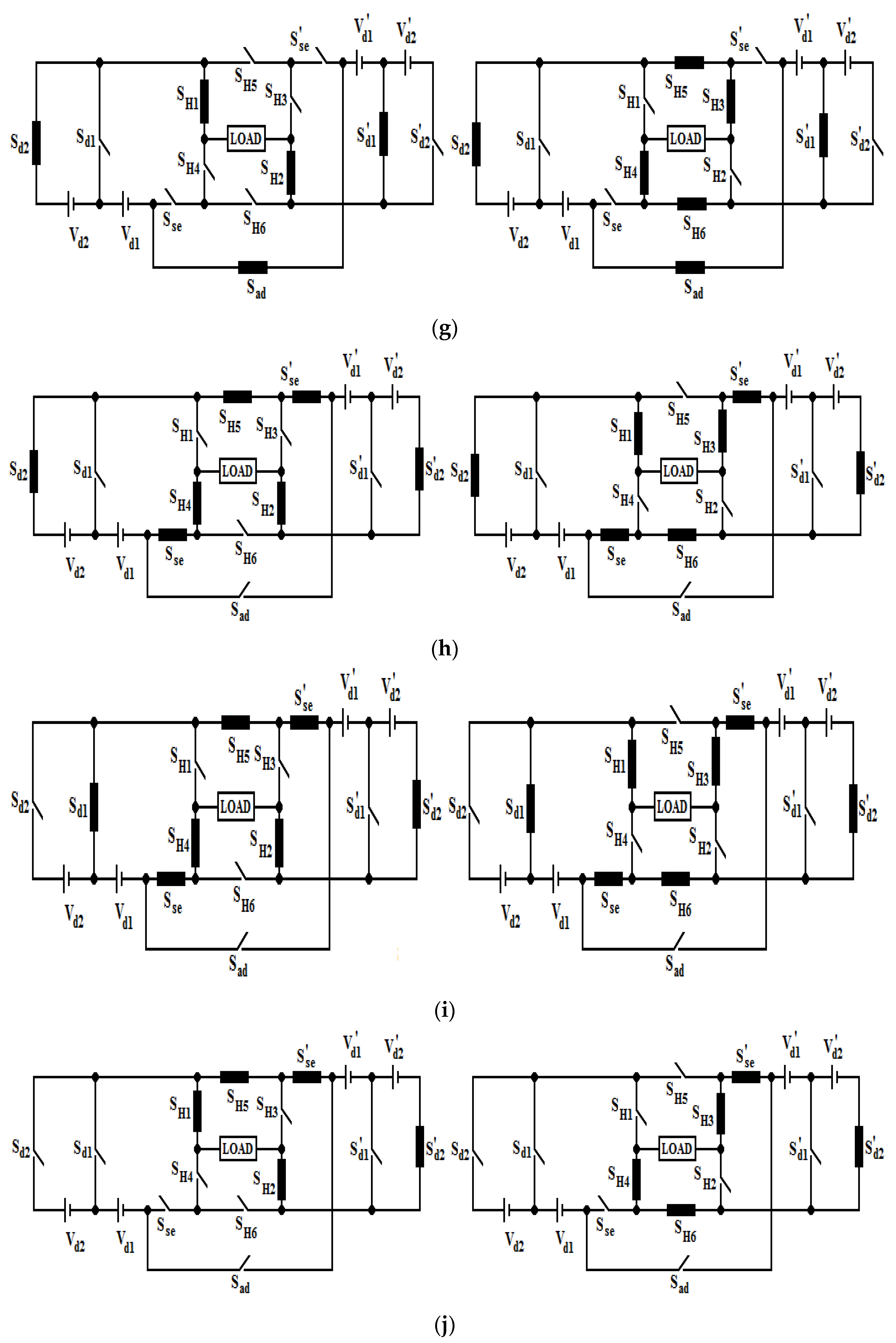
2. Proposed Topology

In recent years, MLIs have had footprints in renewable energy sectors due to their inherent ability to produce good quality pole voltages in terms of small steps through low voltage sources and power structures formulated with fast-switching semiconductor switches tied to utility grids. This structure elevates the pole voltage in a shape closer to a sinusoid, which eliminates low-frequency harmonics naturally without the use of low-pass filters. However, the structures pertaining to outward pole voltage from small voltage steps require a larger number of switching devices with an increase in voltage steps. The conventional MLI structure is limited within the applications in medium voltage ranges, which are put forward to formulate new structures in MLI topology with fewer power components.
In order to produce more voltage levels, a newly developed MLI structure pictured in Figure 1, which comprises a string of isolated DC input sources (Vd1–Vdn) and (Vd1′–Vdn′) on either side of the H-6 inverter to produce all possible values of Vd1. The DC sources (Vd1–Vdn and Vd1′–Vdn′) utilize the switches (Sd1–Sdn & Sd1′–Sdn′) for generating voltage steps, and the switches (SH1-SH6) change the polarity of generated voltage. The voltage source (Vd1) decides the minimum step in the load voltage while the remaining voltage sources (Vd2–Vdn and Vd1′–Vdn′) produce voltage steps in multiples of voltage source magnitude (Vd1) in the output voltage. The switching devices (Sse, Sse′ and Sad) are used to add and subtract the voltage sources (Vd1′–Vdn′) from (Vd1–Vdn). Figure 2 portrays the operating modes to produce different steps of load voltage. The input voltage sources for the developed topology areacquired possibly from PV (photovoltaic) panels or FC (fuel cells) or any other storage elements like capacitors or batteries. In the suggested topology, a maximum of four switches in the level generation side functioning at PWM and three switches in the H-bridge operating at fundamental switching necessitate less switching loss. Hybrid PWM may also be employed to perform PWM operations in H-bridge inverters and fundamental switching in the proposed MLI structure in the proposed hybrid inverter to reduce power loss. The number of voltage sources, switches, and voltage levels are related by (n), [n + 9], and [(6 × n) + 3], where (n > 1) is the number of isolated DC input sources.
Since the proposed structure is an asymmetrical topology, there is a possibility of taking different voltage source values to elucidate the objective of attaining more voltage levels. Nine algorithms have been formulated to derive the values of source voltages to operate in the asymmetrical mode. The algorithms have been coined for the proposed structure with four DC sources (Vd1, Vd2, Vd1′, Vd2′) in a cascaded connection. Table 1 tabulates the mathematical relations pertaining to determiningvarious parameters using proposed voltage source algorithms. The proposed structure has an inherent feature of producing odd/even voltage levels. Using a few modules of the proposed MLI structure with an H-bridge inverter, more voltage steps are produced with fewer power elements compared with conventional MLIs.
The proposed asymmetrical topology has thefreedom to enjoy operations at different input voltage source values, which increases the number of output voltage levels. There are ten different mathematical relations presented to examine the performance of the proposed structure in asymmetrical modes with fewer switching devices, as shown in Table 1. It is observed that the blocking voltage of the switches used in the proposed structure is decided by the input voltage sources connected to produce the desired voltage levels. The suggested algorithms are comprehended with three modular structures with 39 switches and 12 DC sources in a cascaded connection, and the corresponding source voltage values are tabulated in Table 2. The first two methods are omitted for the discussion since the variety of voltage ratios is only two, and the other methods are very interesting in getting a variety of voltage ratios that are more than two. The least source voltage value decides the minimum step voltage in the load terminals, and the proposed relations result in a variety of voltage levels using the proposed structure. It is seen in Table 2 that methods 3 and 5 have voltage values in the order of even numbers, which produce voltage levels of 85 and 81, respectively. Similarly, methods 4 and 6 have voltage ratios in multiples of three and produce voltage levels of 105 and 153, respectively. Methods 7 and 8 produce voltage levels of 169 and 373, respectively, with fewer blocking voltage switches. Method 9 produces a maximum voltage level of 685 for the same number of switches and DC sources as used in methods 1 to 8. It is concluded that the proposed structure is capable of generating voltage levels higher in number with asymmetrical sources, which are acquired from PV or fuel cell sources.
The reliability of the proposed topology is justified by proper comparison with traditional and recent topologies in terms of isolated DC sources, switching devices, gate drivers, and total blocking voltage of the switches. Since the proposed topology involves isolated DC sources, a detailed comparison study is taken by considering similar asymmetrical cascaded MLI topologies with isolated DC sources [14,19,23,26,28]. These topologies are facilitated with a variety of isolated DC sources with asymmetrical voltage values. These methods help in identifying the maximum possible voltage levels that can be generated for given values of stacks (n). Table 3 tabulates the relations to attain various parameters for proposed and recent asymmetrical topologies. The proposed topology with derived algorithm (PA10) shows a larger variation in level generation in a minimum number of stacks compared with recent topologies.
Figure 3 shows the variation of IGBTs for proposed and recent reduced count topologies. In the proposed topology, four isolated DC sources and 13 unidirectional IGBTs are used to formulate a stack (n). The maximum switches in the current conduction path will be half the total switch count. However, the conduction loss can be reduced by facilitating fundamental switching in the H-6 inverter and PWM operations in the switches connected in the DC sources. Figure 3 shows that the proposed MLI needs fewer IGBTs compared with recent topologies. In Figure 4, the proposed topology uses only unidirectional IGBTs, and the gate driver required is proportional to the switches used in the proposed topology. The recent reduced count topologies involve both unidirectional and bidirectional IGBTs and the number of gate drivers required by the recent topologies is high compared with the proposed MLI. The recent topologies are symmetrical and are decided by the variety of voltage sources used. The proposed MLI requires fewerDC sources as the level increases, as authenticated from Figure 5. In some conventional topologies, the DC sources are not completely utilized to produce the voltage levels [28]. The total blocking voltage (TBV) of the proposed topology and recent topologies are measured in terms of the TBV of the proposed topology. It is known from Figure 6 that the topologies [14,19,23,26,28] require switches with a blocking voltage of (5% to 32%) of the proposed topology. As the level increases, the proposed MLI standing voltage of the IGBTs isless compared with the proposed MLI.
The feasibility of the proposed MLI for utility applications suggeststhat it has good efficiency compared with traditional topologies. The proposed topology has better efficiency if it has lesser power loss. The power loss can be reduced by employing hybrid PWM in the proposed topology, the level generation part (IGBTs in DC sources side) switched at PWM and load current reversing in load (IGBTs in the H-6 inverter) performed by fundamental switching at line frequency. The power loss across the IGBT is to be computed during switching and conduction of load current over one switching cycle. The proposed MLI requires fewer IGBTs inthe current conduction path in line with traditional MLIs and four switches perform PWM switching in level generation and four switches with fundamental switching in an H-6 inverter compared with CHBMLI with eight switches for the same number of voltage levels. The switching loss incurred during the shift from off-state voltage/current to conduct current during on-state over one fundamental switching cycle. Similarly, the conduction loss is invariable with switching frequency (fs), and the switching loss increases proportional to (fs).
The switching loss during (Turn-ON and Turn-OFF) of the ‘ith’ switch is given in (1)
P S = j = 1 13 z 1 6 [ ( t o n + t o f f ) × I × V o , j × f ]
where, Ps is switching losses
Ton—on time in sec
Toff—off time in sec
I—Current in Amps
Vo,j—Output voltage in volts
f—Frequency in Hertz
The proposed MLI is portrayed to operate with the 25-level inverter with less switching loss in par with CHBMLI. For the 25-level inverter with equal step values of Vdc, the average switching loss is given in (2)
P S = i = 1 13 z 1 6 [ ( t o n + t o f f ) × I o × V o × f ]
where, IO—Output Current in amps
It is assumed that the ton and toff values are the same in each switch while carrying the load current (Io), therefore the switching loss is approximated in (3) as
P S = γ × V o × f
where γ is constant,
γ = 1 6 ( ( t o n + t o f f ) × I o )
The CHBMLI requires 16 switching devices which are switched at high switching frequency, while the proposed topology requires only three switches that operate at high switching frequency. The ratio of switching loss incurred by proposed topology over CHBMLI is given by
P S ( C H B M L I ) = 16 × γ × V d c × f s
P S ( Pr o p o s e d ) = 4 × γ × V d c × f s
P S ( Pr o p o s e d ) P S ( C H B M L I ) = 1 4

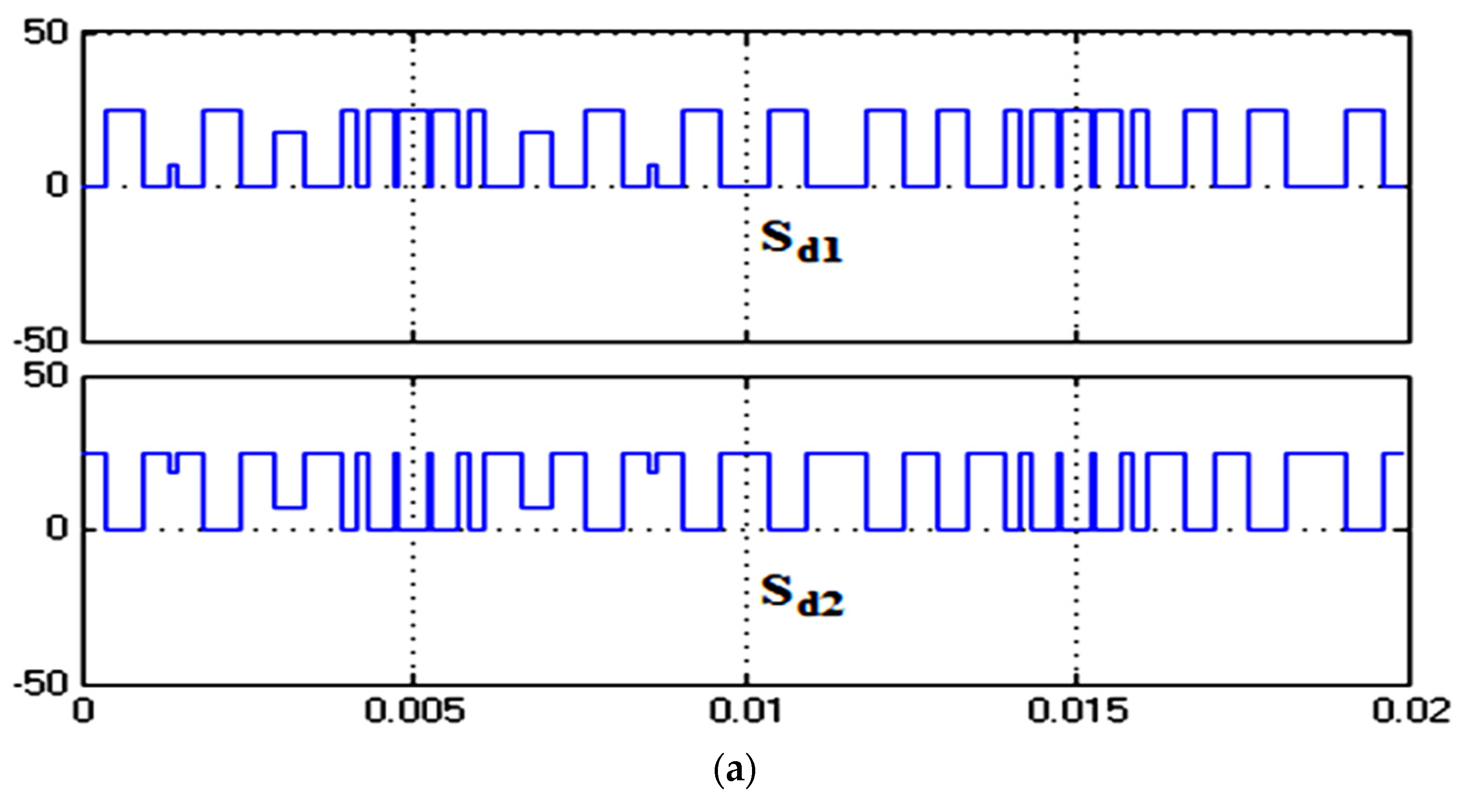
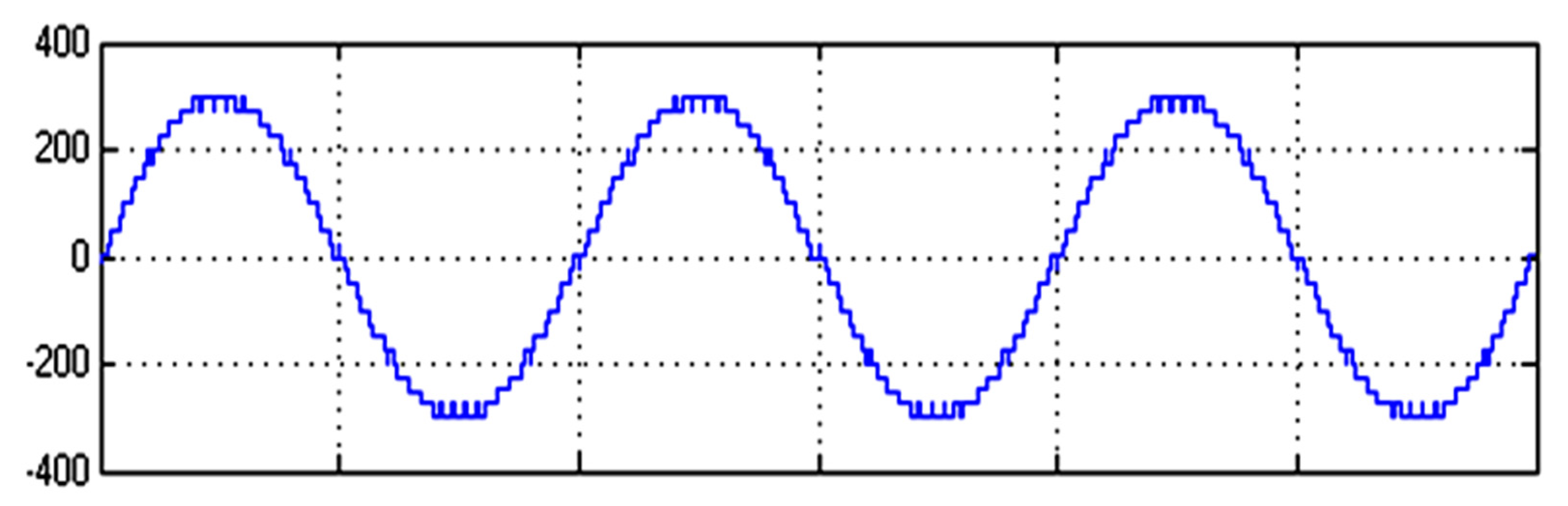
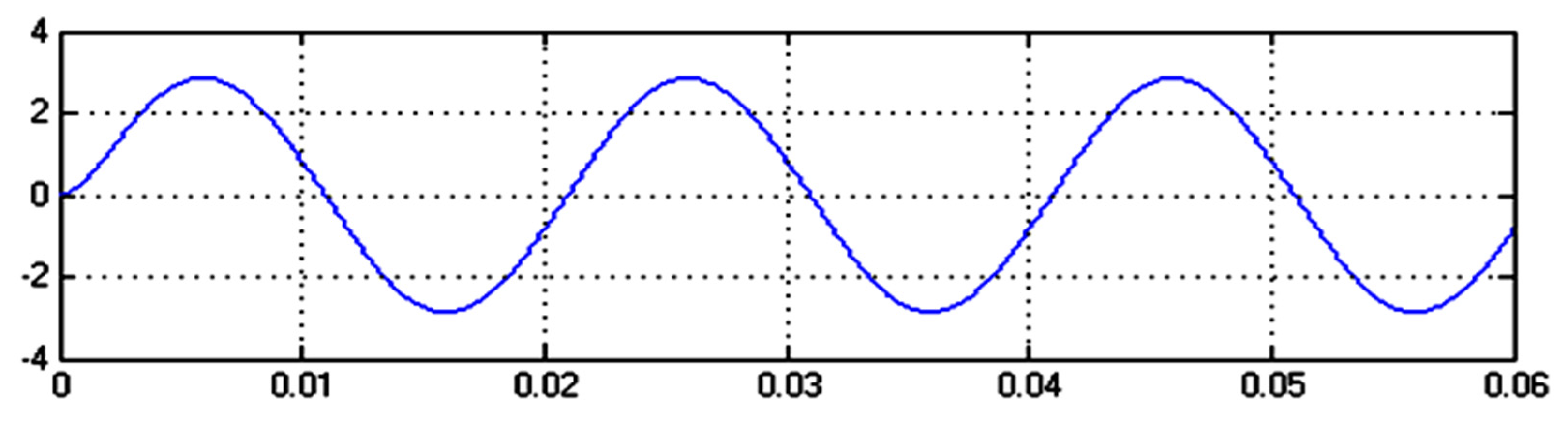
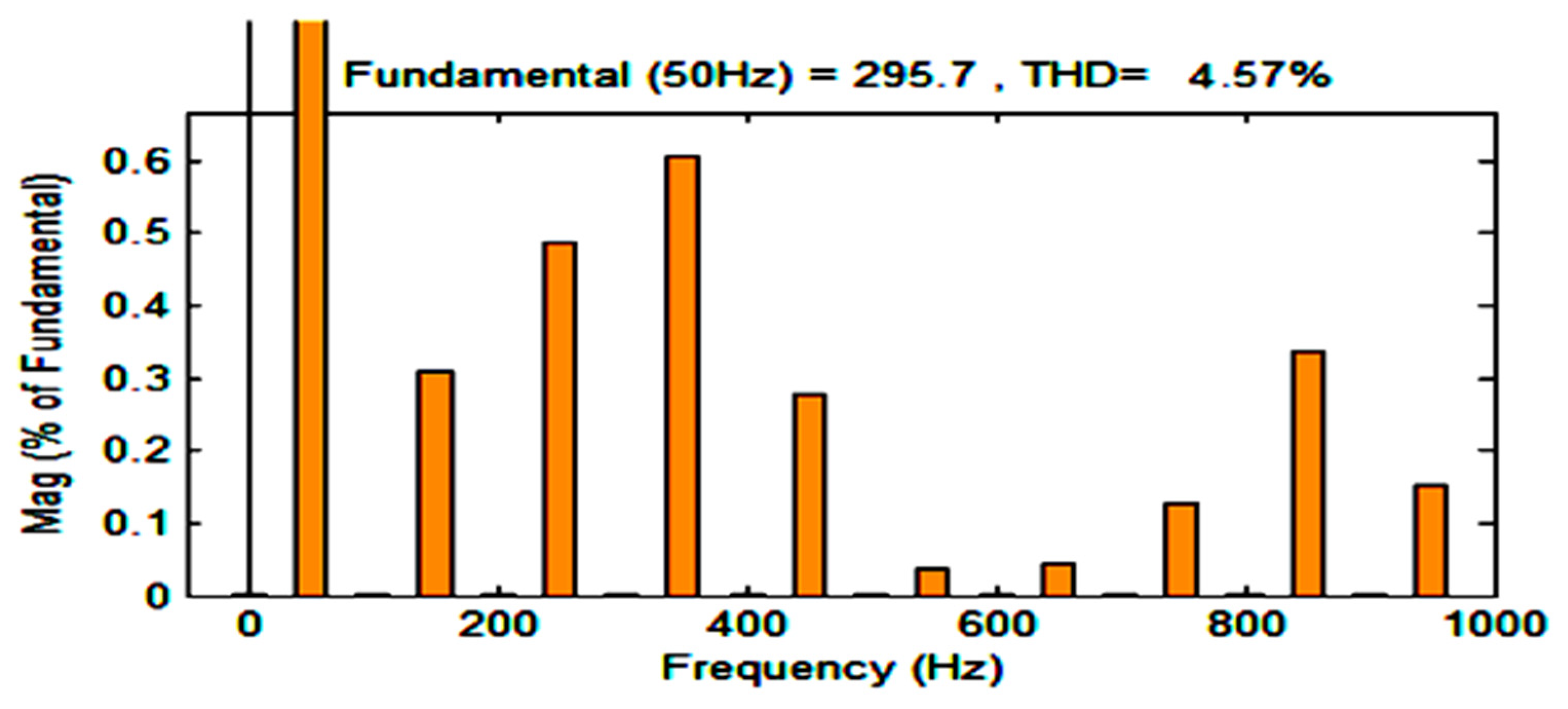
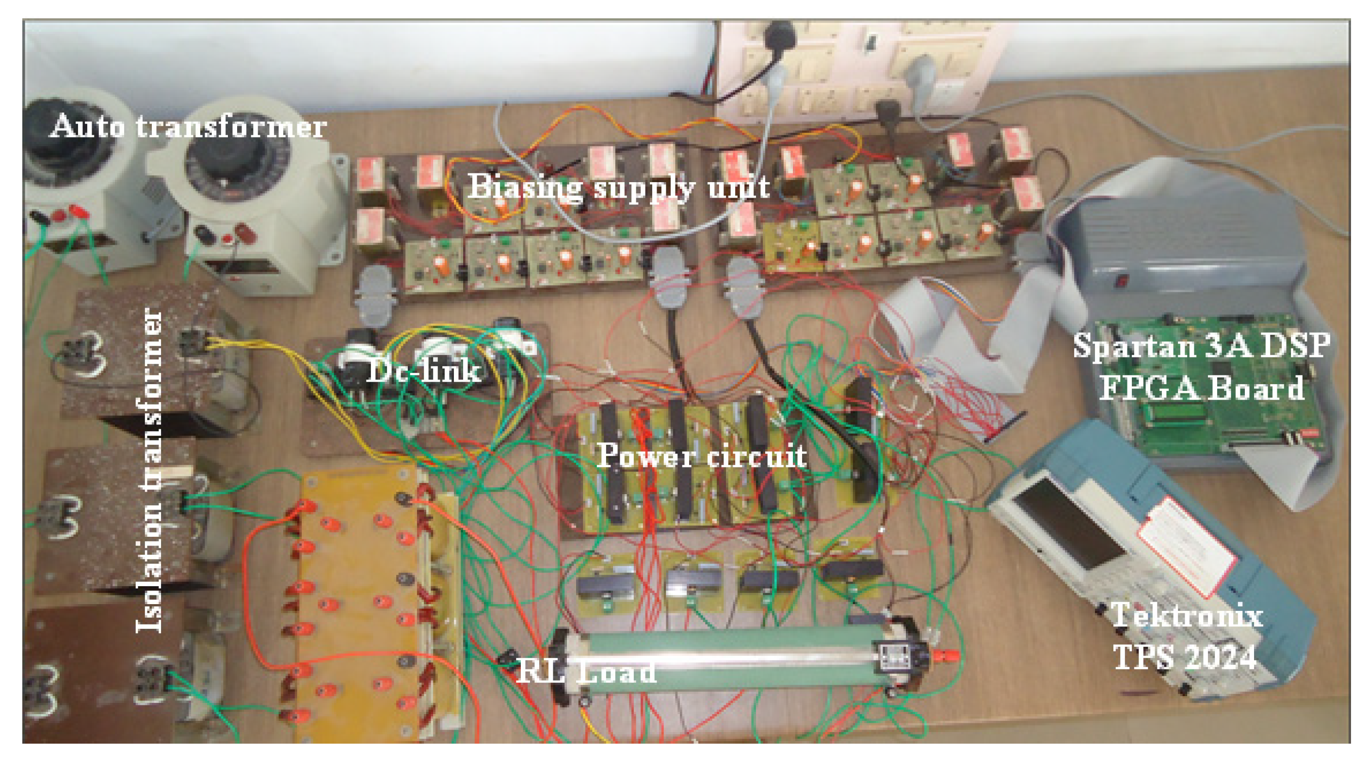
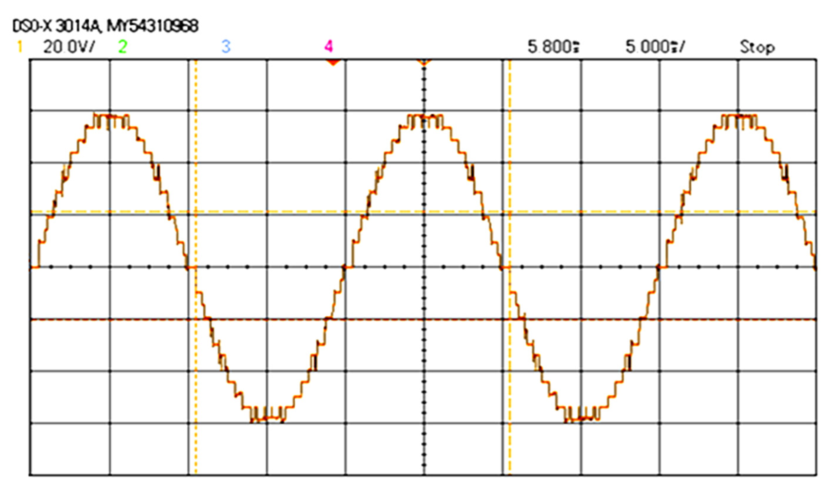
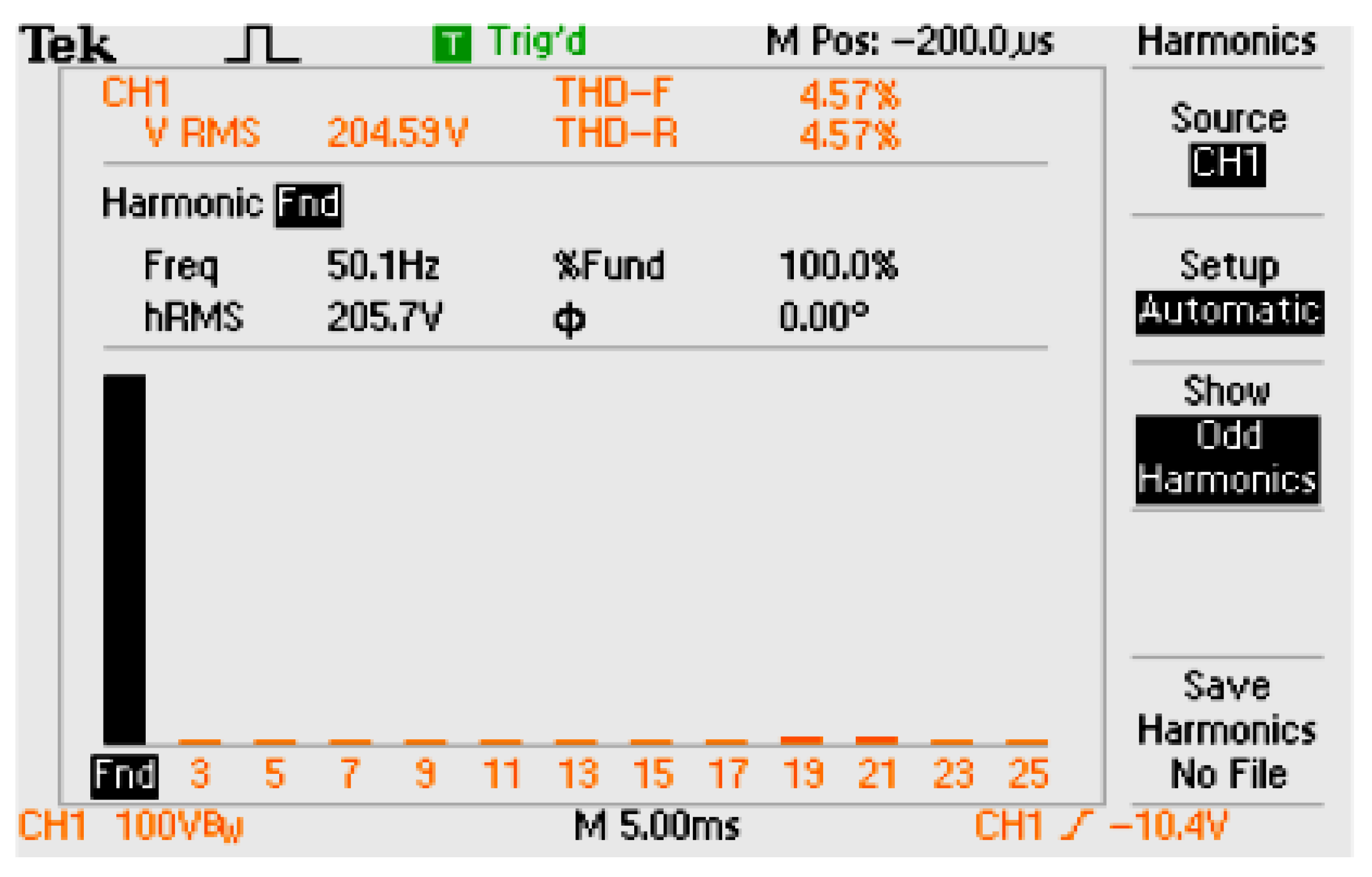
3. Simulation and Experimental Investigation

The operating characteristics of the developed MLI is understood in the Matlab/Simulink environment and the inverter is designed to produce the operating terminal voltage of 300 V (peak) for an RL load of 100 Ω and 100 mH, respectively. The input voltage sources are selected in a variety of values to configure the suggested MLI in an asymmetrical operation. The suggested MLI has the possibility of functioning at either fundamental switching or PWM. The PWM method is predominantly used in industrial applications and the proposed topology is studied with PWM operation. The well-known multicarrier PWM (MCPWM) method is considered for deliberating base PWM pulses, and the required pulses for each level are acquired suitably using logical functions to buffer the required switches to pump PWM modulated stepped voltage waveform in the load terminals. The simulation study is performed to operate the proposed MLI for producing the 25-level inverter with the input voltage parameters of Vd(1,1) = Vd(1,1) = 25 V; Vd(1,1)’ = Vd(1,1)’ = 125 V RL load of 100 Ω and 100 mH, respectively. The simulated response of the proposed asymmetrical MLI is presented in Figure 7, Figure 8 and Figure 9 with voltage stress of the PWM switched IGBTs, output voltage, and inductive load current. From Figure 7, it is understood that the voltage stress on IGBTs is decided by the voltage sources connected to the load in the conduction path. The IGBT (Sse) holds the magnitudes of voltage sources (Vd1′ and Vd2′), and the remaining IGBTs withstand the magnitudes of the voltage sources connected to it. Therefore, the proposed MLI has lower standing voltages at higher voltage levels. It is perceived in Figure 8 that the output voltage has a maximum value of 300 V (peak) and the switching frequency of 2 kHz. The output voltage follows the shape of a sinusoidal and has a THD of 4.57%, which is a relative value to the IEEE 519 standard. The simulated harmonic spectrum is shown in Figure 10. The load current is sinusoidal due to the low-pass filter behavior of the inductive load and has a value of 2 A and THD of 5.42%, respectively.
The proposed MLI is fabricated with similar parameters exercised in the simulation for laboratory prototype testing, depicted in Figure 11. The proposed MLI makes use of several isolated power modules using IGBTs (IRG4BC20SD) and associated driver circuits (IR2110). The MLI is making up for any voltage levels using few IGBT modules and gate driver units. The base PWM and required gating signals stream up the required voltage levels through Digilent Xilinx Spartan 3E-500 FG320 FPGA controller. The onboard clock frequency used for pulse generation is 50 MHz. The design flow postulates the base PWM generation for each level of the 25-level inverter. The data for reference sine is taken at different intervals and formed as Look-uptables (LUTs). A counter is set for acquiring the sine data from a stored memory address. Similarly, for carrier wave generation, a step value is calculated based on the carrier frequency and is added to the base value to generate a triangular carrier. The sine reference and triangular carrier waves are compared to produce the base PWM pulses. The Base PWM pulses are suitably employed to generate required pulses through logical operations for the 25-level inverter. The developed PWM patterns are obtained by writing VHDL coding and a bit file is generated using Xilinx-ISE software. The bit file is downloaded to the FPGA controller through Digilent Adept software. The corresponding output voltage, inductive load current, and harmonic spectrums are displayed in Figure 12, Figure 13 and Figure 14, respectively. The experimental results are displayed in accordance with simulation results.

4. Conclusions

The proposed asymmetrical MLI helps to attain a large number of voltage steps with a reduced number of DC sources, switches, and gate drivers compared with traditional MLIs. A stack of four voltage sources and 13 IGBTs is used to facilitate a new asymmetrical MLI. A few modules are arranged in a cascaded connection to achieve large variations in voltage steps with minimum IGBTs. The ten varieties of voltage source value computation methods are portrayed further to prove the viability of the proposed MLI for practical applications. The proposed MLI enjoys the freedom of replacing isolated DC sources by PV sources or capacitors to open a scope for investigations. The proposed MLI is simulated with traditional PWM and has a choice of switching tohybrid PWM also. The simulated results accumulate the inference from asymmetrical operation to extend the scope for deriving various voltage determination methods. The laboratory test performance is well followed with the simulation studies and concludes that the proposed MLI is well suited for medium voltage and renewable energy applications.

Author Contributions

Conceptualization, A.R. and K.C.; methodology, A.R.; software, E.S.A.; validation, B.C.R., E.S.A. and K.C.; formal analysis, B.C.R.; investigation, A.R.; resources, A.R.; data curation, K.C.; writing—original draft preparation, A.R.; writing—review and editing, B.C.R. and E.S.A.; supervision, E.S.A. and B.C.R.; project administration, K.C.; funding acquisition, K.C. All authors have read and agreed to the published version of the manuscript.

Funding

This research received no external funding.

Data Availability Statement

The data presented in this study are available in article.

Acknowledgments

The authors extend their heartfelt gratitude to the esteemed management, dedicated principal, and diligent Registrar of Arunai Engineering College, Tiruvannamalai, India. Their unwavering support, guidance, and commitment to academic excellence have been invaluable throughout the research process. We are particularly thankful for their encouragement in fostering an environment that promotes learning and research endeavors. This acknowledgement serves as a token of appreciation for their instrumental roles in our academic journey.

Conflicts of Interest

The authors declare no conflict of interest.

References

  1. Ruiz-Gonzalez, A.; Heredia-Larrubia, J.-R.; Meco-Gutierrez, M.J.; Perez-Hidalgo, F.-M. Pulse-Width Modulation Technique with Harmonic Injection in the Modulating Wave and Discontinuous Frequency Modulation for the Carrier Wave for Multilevel Inverters: An Application to the Reduction of Acoustic Noise in Induction Motors. IEEE Access 2023, 11, 40579–40590. [Google Scholar] [CrossRef]
  2. Mondal, S.; Biswas, S.P.; Islam, R.; Muyeen, S.M. A Five-Level Switched-Capacitor Based Transformerless Inverter with Boosting Capability for Grid-Tied PV Applications. IEEE Access 2023, 11, 12426–12443. [Google Scholar] [CrossRef]
  3. Ali, M.; Tayyab, M.; Sarwar, A.; Khalid, M. A Low Switch Count 13-Level Switched-Capacitor Inverter with Hexad Voltage-Boosting for Renewable Energy Integration. IEEE Access 2023, 11, 36300–36308. [Google Scholar] [CrossRef]
  4. Srivastava, A.; Seshadrinath, J. A Single-Phase Seven-Level Triple Boost Inverter for Grid-Connected Transformerless PV Applications. IEEE Trans. Ind. Electron. 2023, 70, 9004–9015. [Google Scholar] [CrossRef]
  5. Mondol, H.; Rahman, A.; Biswas, S.P.; Islam, R.; Kibria, F.; Muttaqi, K.M. A New Integrated Multilevel Inverter Topology for Renewable Energy Transformation. IEEE Trans. Ind. Appl. 2023, 59, 3031–3043. [Google Scholar] [CrossRef]
  6. Li, J.; Chen, J.; Gong, C. An Optimized Reactive Power Compensation Strategy to Extend the Working Range of CHB Multilevel Grid-Tied Inverters. IEEE Trans. Power Electron. 2023, 38, 5500–5512. [Google Scholar] [CrossRef]
  7. Hosseinzadeh, M.A.; Sarebanzadeh, M.; Kennel, R.; Babaei, E.; Rivera, M. New Generalized Circuits for Single-Phase Multisource Multilevel Power Inverter Topologies. IEEE Trans. Power Electron. 2023, 38, 6823–6830. [Google Scholar] [CrossRef]
  8. Tak, N.; Chattopadhyay, S.K.; Chakraborty, C. Single-Sourced Double-Stage Multilevel Inverter for Grid-Connected Solar PV Systems. IEEE Open J. Ind. Electron. Soc. 2022, 3, 561–581. [Google Scholar] [CrossRef]
  9. Junior, S.C.S.; Jacobina, C.B.; Fabricio, E.L.L.; Felinto, A.S. Asymmetric 49-Levels Cascaded MPUC Multilevel Inverter Fed by a Single DC Source. IEEE Trans. Ind. Appl. 2022, 58, 7539–7549. [Google Scholar] [CrossRef]
  10. Meraj, S.T.; Rahman, M.S.A.; Yahaya, N.Z.; Ker, P.J.; Hossain, T.M.; Lipu, M.S.H.; Muttaqi, K.M.; Hannan, M.A. A Pencil Shaped 9-Level Multilevel Inverter with Voltage Boosting Ability: Configuration and Experimental Investigation. IEEE Access 2022, 10, 111310–111321. [Google Scholar] [CrossRef]
  11. Akbari, A.; Ebrahimi, J.; Jafarian, Y.; Bakhshai, A. A Multilevel Inverter Topology with an Improved Reliability and a Reduced Number of Components. IEEE J. Emerg. Sel. Top. Power Electron. 2022, 10, 553–563. [Google Scholar] [CrossRef]
  12. Mondol, H.; Biswas, S.P.; Rahman, A.; Islam, R.; Mahfuz-Ur-Rahman, A.M.; Muttaqi, K.M. A New Hybrid Multilevel Inverter Topology with Level Shifted Multicarrier PWM Technique for Harvesting Renewable Energy. IEEE Trans. Ind. Appl. 2022, 58, 2574–2585. [Google Scholar] [CrossRef]
  13. Maamar, A.E.T.; Kermadi, M.; Helaimi, M.; Taleb, R.; Mekhilef, S. An Improved Single-Phase Asymmetrical Multilevel Inverter Structure with Reduced Number of Switches and Higher Power Quality. IEEE Trans. Circuits Syst. II Express Briefs 2021, 68, 2092–2096. [Google Scholar] [CrossRef]
  14. Kakar, S.; Ayob, S.B.M.; Iqbal, A.; Nordin, N.M.; Bin Arif, M.S.; Gore, S. New Asymmetrical Modular Multilevel Inverter Topology with Reduced Number of Switches. IEEE Access 2021, 9, 27627–27637. [Google Scholar] [CrossRef]
  15. Samanbakhsh, R.; Ibanez, F.M.; Koohi, P.; Martin, F. A New Asymmetric Cascaded Multilevel Converter Topology with Reduced Voltage Stress and Number of Switches. IEEE Access 2021, 9, 92276–92287. [Google Scholar] [CrossRef]
  16. Dhanamjayulu, C.; Prasad, D.; Padmanaban, S.; Maroti, P.K.; Holm-Nielsen, J.B.; Blaabjerg, F. Design and Implementation of Seventeen Level Inverter with Reduced Components. IEEE Access 2021, 9, 16746–16760. [Google Scholar] [CrossRef]
  17. Isazadeh, A.; Adabi, J.; Rezanejad, M.; Adabi, M.E. Operation and Control of a Grid-Connected Asymmetrical Cascaded Multilevel Inverter. IEEE J. Emerg. Sel. Top. Power Electron. 2021, 9, 1614–1623. [Google Scholar] [CrossRef]
  18. Khoun-Jahan, H. University of tabriz switched capacitor based cascaded half-bridge multilevel inverter with voltage boosting feature. CPSS Trans. Power Electron. Appl. 2021, 6, 63–73. [Google Scholar] [CrossRef]
  19. Babaei, E.; Laali, S.; Bayat, Z. A Single-Phase Cascaded Multilevel Inverter Based on a New Basic Unit with Reduced Number of Power Switches. IEEE Trans. Ind. Electron. 2015, 62, 922–929. [Google Scholar] [CrossRef]
  20. Kumar, A.; Wang, Y.; Raghuram, M.; Pilli, N.K.; Singh, S.K.; Pan, X.; Xiong, X. A Generalized Switched Inductor Cell Modular Multilevel Inverter. IEEE Trans. Ind. Appl. 2020, 56, 507–518. [Google Scholar] [CrossRef]
  21. Rao, B.N. National institute of technology karnataka development of cascaded multilevel inverter based active power filter with reduced transformers. CPSS Trans. Power Electron. Appl. 2020, 5, 147–157. [Google Scholar] [CrossRef]
  22. Vasu, R.; Chattopadhyay, S.K.; Chakraborty, C. Asymmetric Cascaded H-Bridge Multilevel Inverter with Single DC Source per Phase. IEEE Trans. Ind. Electron. 2020, 67, 5398–5409. [Google Scholar] [CrossRef]
  23. Gohari, A.; Afjei, E.S.; Torkaman, H. Novel Symmetric Modular Hybrid Multilevel Inverter with Reduced Number of Semiconductors and Low-Voltage Stress Across Switches. IEEE J. Emerg. Sel. Top. Power Electron. 2020, 8, 4297–4305. [Google Scholar] [CrossRef]
  24. Ponnusamy, P.; Sivaraman, P.; Almakhles, D.J.; Padmanaban, S.; Leonowicz, Z.; Alagu, M.; Ali, J.S.M. A New Multilevel Inverter Topology with Reduced Power Components for Domestic Solar PV Applications. IEEE Access 2020, 8, 187483–187497. [Google Scholar] [CrossRef]
  25. Roy, T.; Sadhu, P.K.; Dasgupta, A. Cross-Switched Multilevel Inverter Using Novel Switched Capacitor Converters. IEEE Trans. Ind. Electron. 2019, 66, 8521–8532. [Google Scholar] [CrossRef]
  26. Zamiri, E.; Moradzadeh, M.; Barzegarkhoo, R.; Hamkari, S.; Sabahi, M. Cascaded Multilevel Inverters Using Proposed Series Sub-multilevel Basic Blocks with Reduced Switching Devices. Electr. Power Compon. Syst. 2017, 45, 1691–1704. [Google Scholar] [CrossRef]
  27. Chittathuru, D.; Padmanaban, S.; Prasad, R. Design and Implementation of Asymmetric Cascaded Multilevel Inverter with Optimal Components. Electr. Power Compon. Syst. 2021, 49, 361–374. [Google Scholar] [CrossRef]
  28. Kamani, P.L.; Mulla, M.A. A Home-type (H-type) Cascaded Multilevel Inverter with Reduced Device Count: Analysis and Implementation. Electr. Power Compon. Syst. 2019, 47, 1691–1704. [Google Scholar] [CrossRef]
  29. Siddique, M.D.; Rawa, M.; Mekhilef, S.; Shah, N.M. A new cascaded asymmetrical multilevel inverter based on switched dc voltage sources. Int. J. Electr. Power Energy Syst. 2021, 128, 106730. [Google Scholar] [CrossRef]
  30. Kumar, D.; Raj, R.A.; Nema, R.K.; Nema, S. A Novel Higher Level Symmetrical and Asymmetrical Multilevel Inverter for Solar Energy Environment. IETE J. Res. 2022, 68, 3670–3682. [Google Scholar] [CrossRef]
Figure 1. Proposed MLI topology.
Symmetry 16 00072 g001
Figure 2. (a)Equivalent circuit of operating mode ± (Vd1). (b) Equivalent circuit of operating mode ± (Vd1 + Vd2). (c) Equivalent circuit of operating mode ± (Vd1′ − (Vd1 + Vd2)). (d) Equivalent circuit of operating mode ± (Vd1′ − (Vd1)).(e) Equivalent circuit of operating mode ± (Vd1′). (f) Equivalent circuit of operating mode ± (Vd1′ + (Vd1)). (g) Equivalent circuit of operating mode ± (Vd1′ + Vd1 + Vd2). (h) Equivalent circuit of operating mode ± ((Vd1′ + Vd2′) − (Vd1 + Vd2)). (i) Equivalent circuit of operating mode ± ((Vd1′ + Vd2′)−(Vd1)). (j) Equivalent circuit of operating mode ± ((Vd1′ + Vd2′)). (k) Equivalent circuit of operating mode ± ((Vd1′ + Vd2′) + (Vd1)). (l) Equivalent circuit of operating mode ± ((Vd1′ + Vd2′) + (Vd1 + Vd2)).
Symmetry 16 00072 g002aSymmetry 16 00072 g002bSymmetry 16 00072 g002cSymmetry 16 00072 g002d
Figure 3. Variation of IGBTs between proposed and recent MLIs for the 625-level inverter [14,19,23,26,28].
Symmetry 16 00072 g003
Figure 4. Variation of gate drivers between proposed and recent MLIs for the 625-level inverter [14,19,23,26,28].
Symmetry 16 00072 g004
Figure 5. Variation of isolated DC sources between proposed and recent MLIs for the 625-level inverter [14,19,23,26,28].
Symmetry 16 00072 g005
Figure 6. Variation of total blocking voltage (TBV) between proposed and recent MLIs for the 625-level inverter [14,19,23,26,28].
Symmetry 16 00072 g006
Figure 7. (a) Voltage stress across IBGTs—Sd1 & Sd2. (b) Voltage stress across IBGTs—Sd1′ & Sd2′. (c) Voltage stress across IBGTs—Sse & Sse’.
Symmetry 16 00072 g007aSymmetry 16 00072 g007b
Figure 8. Output voltage for the 25-level inverter.
Symmetry 16 00072 g008
Figure 9. Inductive load current for the 25-level inverter.
Symmetry 16 00072 g009
Figure 10. Simulation—harmonic spectra for the 25-level inverter.
Symmetry 16 00072 g010
Figure 11. Hardware proofofconcept.
Symmetry 16 00072 g011
Figure 12. Load voltage waveform for the25-level inverter.
Symmetry 16 00072 g012
Figure 13. Load current waveform for the25-level inverter.
Symmetry 16 00072 g013
Figure 14. Hardware—harmonic spectra for the 25-level inverter.
Symmetry 16 00072 g014
Table 1. Mathematical relations to determine various parameters using proposed voltage source algorithms.
AlgorithmVoltage Sources Values and Max. Output VoltageNo. of Voltage LevelsBlocking Voltage
Proposed Algorithm 1 V d ( 1 , j ) = V d ( 2 , j ) = V d ( 1 , j ) = V d ( 2 , j ) = V dc
V om = 4 nV dc
(8 × n) + 127nVdc
Proposed Algorithm 2 V d ( 1 , j ) = V d ( 2 , j ) = V dc ; V d ( 1 , j ) = V d ( 2 , j ) = 2 V dc
V max = 6 nV dc
(12 × n) + 144nVdc
Proposed Algorithm 3 V d ( 1 , 1 ) = V d ( 2 , 1 ) = V dc ; V d ( 1 , 1 ) = V d ( 2 , 1 ) = 2 V dc
V d ( 1 , j ) = V d ( 2 , j ) = V d ( 1 , j ) = V d ( 2 , j ) = 2 j 1 V dc
V max = 6 j = 1 n 2 j 1 V dc
12 j = 1 n 2 j 1 + 1 44Vdc; n = 1
[44 + (5 × 2n) + (17 × 2n − 1)] × Vdc; n > 1
Proposed Algorithm 4 V d ( 1 , 1 ) = V d ( 2 , 1 ) = V d ( 1 , 1 ) = V d ( 2 , 1 ) = V dc
V d ( 1 , j ) = V d ( 2 , j ) = V d ( 1 , j ) = V d ( 2 , j ) = 3 j 1 V dc
V max = 4 j = 1 n 3 j 1 V dc
8 j = 1 n 3 j 1 + 1 27Vdc; n = 1
27 × [1 + 3n − 1] × Vdc; n > 1
Proposed Algorithm 5 V d ( 1 , 1 ) = V d ( 2 , 1 ) = V d ( 1 , 1 ) = V d ( 2 , 1 ) = V dc
V d ( 1 , j ) = V d ( 2 , j ) = 2 j 1 V dc ; V d ( 1 , j ) = V d ( 2 , j ) = 2 V d ( 1 , j )
V max = 4 V dc ; n = 1 V max = 6 j = 2 n ( 2 j 1 + 4 ) V dc ; n 1
12 j = 2 n 2 j 1 + 9 ; n 1 27Vdc; n = 1
[27 + (22 × 2n] × Vdc; n > 1
Proposed Algorithm 6 V d ( 1 , 1 ) = V d ( 2 , 1 ) = V d ( 1 , 1 ) = V d ( 2 , 1 ) = V dc
V d ( 1 , j ) = V d ( 2 , j ) = 3 j 1 V dc ; V d ( 1 , j ) = V d ( 2 , j ) = 2 V d ( 1 , j )
V max = 4 V dc ; n = 1 V max = 6 j = 2 n ( 3 j 1 + 4 ) V dc ; n 1
12 j = 2 n 3 j 1 + 9 ; n 1 27Vdc; n = 1
[27 + (44 × 3n − 1] × Vdc; n > 1
Proposed Algorithm 7 V d ( 1 , 1 ) = V d ( 2 , 1 ) = V d ( 1 , 1 ) = V d ( 2 , 1 ) = V dc
V d ( 1 , j ) = V d ( 2 , j ) = V d ( 1 , j ) = V d ( 2 , j ) = 4 j 1 V dc
V max = 4 j = 1 n 4 j 1 V dc
8 j = 1 n 4 j 1 + 1 34Vdc; n = 1
27 × [1 + 4n − 1] × Vdc; n > 1
Proposed Algorithm 8 V d ( 1 , j ) = V d ( 2 , j ) = 5 j 1 V dc ; V d ( 1 , j ) = V d ( 2 , j ) = ( 2 × 5 j 1 ) V dc
V max = 6 j = 2 n ( 5 j 1 ) V dc
12 j = 1 n 5 j 1 + 1 [44 × 5n − 1] × Vdc
Proposed Algorithm 9 V d ( 1 , j ) = V d ( 2 , j ) = 7 j 1 V dc ; V d ( 1 , j ) = V d ( 2 , j ) = ( 2 × 7 j 1 ) V dc
V max = 6 j = 2 n ( 7 j 1 ) V dc
12 j = 1 n 7 j 1 + 1 [44 × 7n − 1] × Vdc
Proposed Algorithm 10 V d ( 1 , j ) = V d ( 2 , j ) = 2 5 j 1 V dc ; V d ( 1 , j ) = V d ( 2 , j ) = ( 5 × 25 j 1 ) V dc
V max = 12 j = 2 n ( 25 j 1 ) V dc
25 n [95 × 25n − 1] × Vdc
Table 2. Determination of values of voltage sources using derived algorithms.
StagesPA3PA4PA5PA6PA7PA8PA9PA10
I (S = 13) Vd(1,1) = Vdc
Vd(2,1) = Vdc
Vd(1,1)’ = 2Vdc
Vd(2,1)’ = 2Vdc
Vd(1,1) = Vdc
Vd(2,1) = Vdc
Vd(1,1)’ = Vdc
Vd(2,1)’ = Vdc
Vd(1,1) = Vdc
Vd(2,1) = Vdc
Vd(1,1)’ = Vdc
Vd(2,1)’ = Vdc
Vd(1,1) = Vdc
Vd(2,1) = Vdc
Vd(1,1)’ = Vdc
Vd(2,1)’ = Vdc
Vd(1,1) = Vdc
Vd(2,1) = Vdc
Vd(1,1)’ = Vdc
Vd(2,1)’ = Vdc
Vd(1,1) = Vdc
Vd(2,1) = Vdc
Vd(1,1)’ = 2Vdc
Vd(2,1)’ = 2Vdc
Vd(1,1) = Vdc
Vd(2,1) = Vdc
Vd(1,1)’ = 2Vdc
Vd(2,1)’ = 2Vdc
Vd(1,1) = Vdc
Vd(2,1) = Vdc
Vd(1,1)’ = 5Vdc
Vd(2,1)’ = 5Vdc
III (S = 39) Vd(1,1) = Vdc
Vd(2,1) = Vdc
Vd(1,1)’ = 2Vdc
Vd(2,1)’ = 2Vdc
Vd(1,2) = 2Vdc
Vd(2,2) = 2Vdc
Vd(1,2)’ = 4Vdc
Vd(2,2)’ = 4Vdc
Vd(1,3) = 4Vdc
Vd(2,3) = 4Vdc
Vd(1,3)’ = 8Vdc
Vd(2,3)’ = 8Vdc
Vd(1,1) = Vdc
Vd(2,1) = Vdc
Vd(1,1)’ = Vdc
Vd(2,1)’ = 3Vdc
Vd(1,2) = 3Vdc
Vd(2,2) = 3Vdc
Vd(1,2)’ = 3Vdc
Vd(2,2)’ = 3Vdc
Vd(1,3) = 9Vdc
Vd(2,3) = 9Vdc
Vd(1,3)’ = 9Vdc
Vd(2,3)’ = 9Vdc
Vd(1,1) = Vdc
Vd(2,1) = Vdc
Vd(1,1)’ = Vdc
Vd(2,1)’ = Vdc
Vd(1,2) = 2Vdc
Vd(2,2) = 2Vdc
Vd(1,2)’ = 4Vdc
Vd(2,2)’ = 4Vdc
Vd(1,3) = 4Vdc
Vd(2,3) = 4Vdc
Vd(1,3)’ = 8Vdc
Vd(2,3)’ = 8Vdc
Vd(1,1) = Vdc
Vd(2,1) = Vdc
Vd(1,1)’ = Vdc
Vd(2,1)’ = Vdc
Vd(1,2) = 3Vdc
Vd(2,2) = 3Vdc
Vd(1,2)’ = 6Vdc
Vd(2,2)’ = 6Vdc
Vd(1,3) = 9Vdc
Vd(2,3) = 9Vdc
Vd(1,3)’ = 18Vdc
Vd(2,3)’ = 18Vdc
Vd(1,1) = Vdc
Vd(2,1) = Vdc
Vd(1,1)’ = Vdc
Vd(2,1)’ = Vdc
Vd(1,2) = 4Vdc
Vd(2,2) = 4Vdc
Vd(1,2)’ = 4Vdc
Vd(2,2)’ = 4Vdc
Vd(1,3) = 16Vdc
Vd(2,3) = 16Vdc
Vd(1,3)’ = 16Vdc
Vd(2,3)’ = 16Vdc
Vd(1,1) = Vdc
Vd(2,1) = Vdc
Vd(1,1)’ = 2Vdc
Vd(2,1)’ = 2Vdc
Vd(1,2) = 5Vdc
Vd(2,2) = 5Vdc
Vd(1,2)’ = 10Vdc
Vd(2,2)’ = 10Vdc
Vd(1,3) = 25Vdc
Vd(2,3) = 25Vdc
Vd(1,3)’ = 50Vdc
Vd(2,3)’ = 50Vdc
Vd(1,1) = Vdc
Vd(2,1) = Vdc
Vd(1,1)’ = 2Vdc
Vd(2,1)’ = 2Vdc
Vd(1,2) = 7Vdc
Vd(2,2) = 7Vdc
Vd(1,2)’ = 14Vdc
Vd(2,2)’ = 14Vdc
Vd(1,3) = 49Vdc
Vd(2,3) = 49Vdc
Vd(1,3)’ = 98Vdc
Vd(2,3)’ = 98Vdc
Vd(1,1) = Vdc
Vd(2,1) = Vdc
Vd(1,1)’ = 5Vdc
Vd(2,1)’ = 5Vdc
Vd(1,2) = 25Vdc
Vd(2,2) = 25Vdc
Vd(1,2)’ = 125Vdc
Vd(2,2)’ = 125Vdc
Vd(1,3) = 625Vdc
Vd(2,3) = 625Vdc
Vd(1,3)’ = 3125Vdc
Vd(2,3)’ = 3125Vdc
Table 3. Mathematical relations to attain various design parameters.
Ref.IGBTsGate DriversDC SourcesTBVLevels
1410n9n4n33n16n + 1
195n + 65n + 63n + 17(2(n + 2)) − 22(2(n + 3)) − 5
236n + 86n + 74n + 1144n + 12.512n + 13
268n8n3n2(7n − 1)7n
2810n9n4n17(15n − 1)/715n
Proposed MLI (PA10)13n13n4n95(25(n − 1))25n
Disclaimer/Publisher’s Note: The statements, opinions and data contained in all publications are solely those of the individual author(s) and contributor(s) and not of MDPI and/or the editor(s). MDPI and/or the editor(s) disclaim responsibility for any injury to people or property resulting from any ideas, methods, instructions or products referred to in the content.

