Article

Symmetric and Asymmetric Crisscross Augmented Ladder Multilevel Inverter with Fuzzy Logic Controller Optimization

by
Parimala Arumugam
1,*,
Srinath Subbaraman
2 and
Kannan Chandrasekaran
1
1
Arunai Engineering College, Tiruvannamalai 606603, India
2
Velammal Engineering College, Chennai 600066, India
*
Author to whom correspondence should be addressed.
Symmetry 2023, 15(7), 1366; https://doi.org/10.3390/sym15071366
Submission received: 9 June 2023 / Revised: 29 June 2023 / Accepted: 30 June 2023 / Published: 5 July 2023
(This article belongs to the Section Engineering and Materials)

Abstract

:
This research article presents a modified novel crisscross augmented ladder (CCAL) structured multilevel inverter (MLI). MLIs can be operated in symmetric and asymmetric binary and ternary voltage ratios. The modified structure comprises a generalized unit (CCAL) and an extendable structure; this structure can be extended to generate more stair case waveform. The foremost benefit of this modified structure is to curb the conduction path of active switches. The utilized structure uses only four active conduction paths in all modes. However, an MLI has complexity, such as a higher number of switches and bulky controlling driver circuits which need superior controls. This article suggests a prominent solution for the above issues. The subtle CCAL is a governed multicarrier pulse width modulation scheme with the savvy fuzzy logic controller and, therefore, added benefits, such as lower switch stress, lower switching loss, and lower dv/dt stress. Hitherto, many topologies are emerging to curb the component count reduction structure; among them it is an attempt to curtail the active conduction path. The working capability of the presented system is substantiated with a simulation study carried out in MATLAB R2017a and viability hardware (Xilinx FPGA) proof of concept to validate the effectiveness.

1. Introduction

Multilevel inverters have been the prevailing topologies in industrial applications for the last four decades, with much research still on going. In recent years, the demand for multi-level inverters has grown substantially in high-voltage and high-power applications such as industrial drives, e-vehicles, renewable energy conversion systems, UPS systems etc. [1]. Archetypally, the complexity of the circuit increases, which leads to an increase in the step levels. The common mode voltage elimination technique is reported to have a lower switch count, as presented in [2]. Cascading the 1-phase sub multilevel converter module with a full-bridge produces 49 level output with a reduced switch count, a smaller number of separate dc sources SDC’s, and a reduction in converter cost, and it occupies a smaller area [3]. Among many topologies, cascading the diode clamped inverter and low voltage conventional inverter can generate 19 levels with a lower number of switches, which assures a good quality output with low THD [4]. Further, a new innovative topology to cater to the bi-directional power flow is carried out with a series of parallel switched multi-level dc link topology employed with sub harmonic PWM technique, which has good sinusoidal output [5]. Besides the common MLIs, the new hybrid symmetric and asymmetric topologies, which handle high power with reduced switch count, were proposed in [6,7]. The injection of third harmonics to cascaded H bridge multilevel inverter CHBMLI reduces 75% of dc link capacitance, and is the effective method of implementation without any excess components [8,9]. To overcome the limitations of the traditional MLI, the cross switched MLI using the switched capacitors with symmetric and asymmetric fashion reduces the TSV and stress on the power switches. This SCMLI generates 37 level output and is suitable for drive utilities, PV based pumping system, and in UPS system [10,11]. The new variant of the MLI topology based on the crisscross technique in the cascaded semi half bridge aims to produce a higher voltage level with reduced standing voltage. This arrangement has a reduced switch count with 21 level output [12] DSTATCOM based on CSMLI, and is presented with an effective voltage balancing control scheme which reduces the harmonics and is suitable for this application [13]. Low total standing voltage TSV on switches can be lengthy and increase the number of levels [14]. Furthermore, peak inverse voltage PIV is lower, with a reduction in voltage drop and power loss [15]. New innovative topologies, with the transformer less distribution static synchronous compensator three dissimilar modules, have been suggested for MLIs: stipulation based sources insertion topology; level count increasing topology; and inter-linking H-bridge topology, along with SDC’s yields 15 levels with component waning [16]. Cross-switched multilevel inverter topology does not uses high voltage switches and achieves the lowest standing voltage [17]. CHBMLI with FLC and PI controller effectively reduces the THD by employing a level shifting phase disposition pulse width modulation LS-PD-PWM technique, generating 5 and 9 levels [18]. A new E type module for an asymmetrical MLI produces 13 levels with 10 switches, which can have low voltage stress employed with selective harmonic elimination pulse width modulation SHEPWM, achieves high quality output [19]. A level dependent sources concoction multilevel inverter (LDSCMLI) can also utilize fewer switches with minimal common mode voltage. Low EMI with the capability to medium/high voltage from low voltage sources is presented in [20]. A blend of single-phase T-Type inverter and an H-Bridge module with sub switches has less TSV, less THD, utilizes fewer power switches, and can produce17 levels [21]. A blend of a single-phase T-Type inverter and an H-Bridge module form an MLI structure formed with sub switches [22]. A new MLI structure, with lower voltage rating components is used to overcome the complexity in conventional multilevel inverter [23,24]. A new produce of MLI with lower blocking voltage and higher number voltage level is proposed with SHE technique [25]. A novel multilevel inverter with fewer switches is developed with a modification of conventional diode clamped inverter for industrial applications [26]. A single-phase power factor corrector (PFC) is employed with a fuzzy logic controller to overcome cost effect [27].
In this article, a novel MLI topology adopted with multicarrier pulse width modulation technique and FLC controller is presented and compared. The proposed topology is extendable and enabled to increase the levels. This paper is organized as follows: Section 2 demonstrates the planned topology with its generalized structure along with the operating modules. The modulation and control strategy explaining the operation of the fuzzy logic controller is described in Section 3. Section 4 presents the simulation and experimental investigations, with the comparative study with the other topologies in both configurations. The conclusion is presented in Section 5.

2. Proposed CCAL Topology

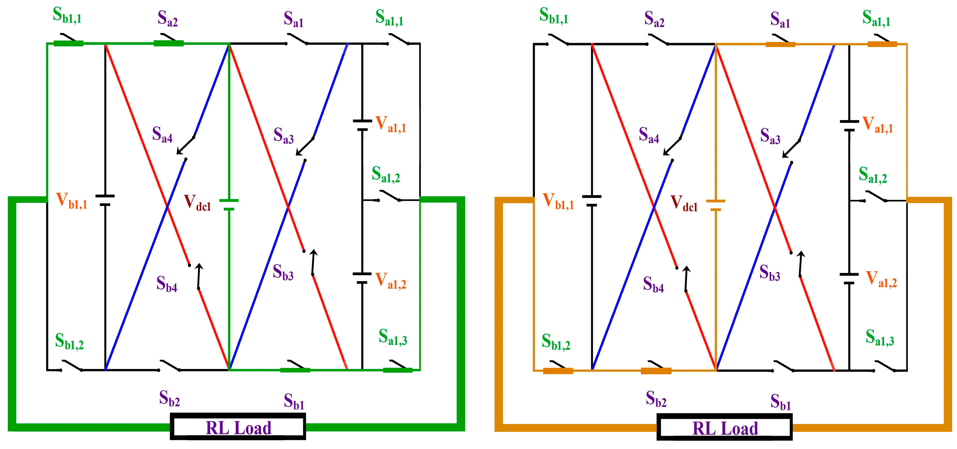
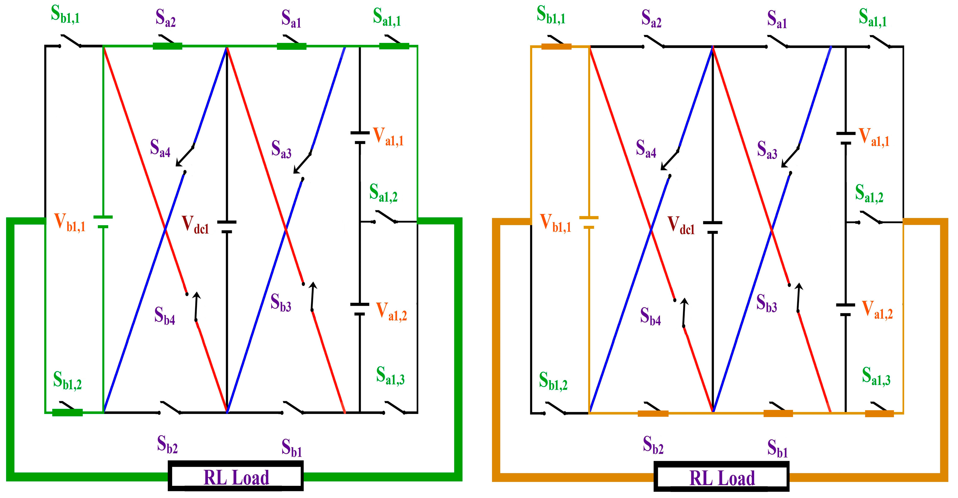
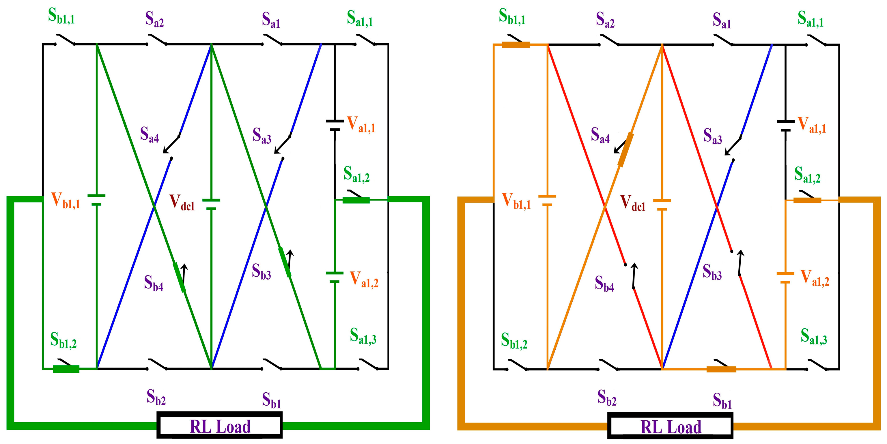
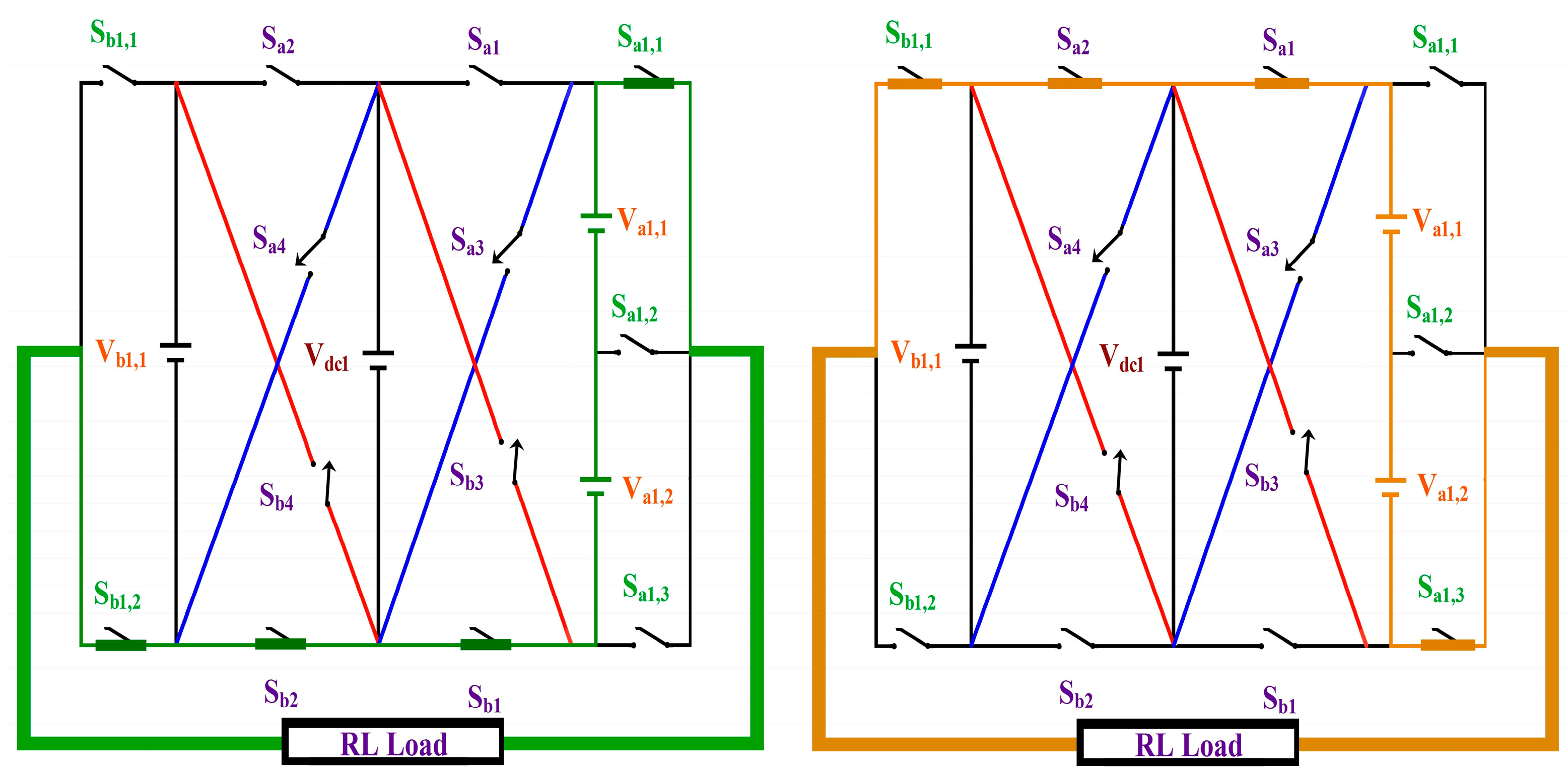
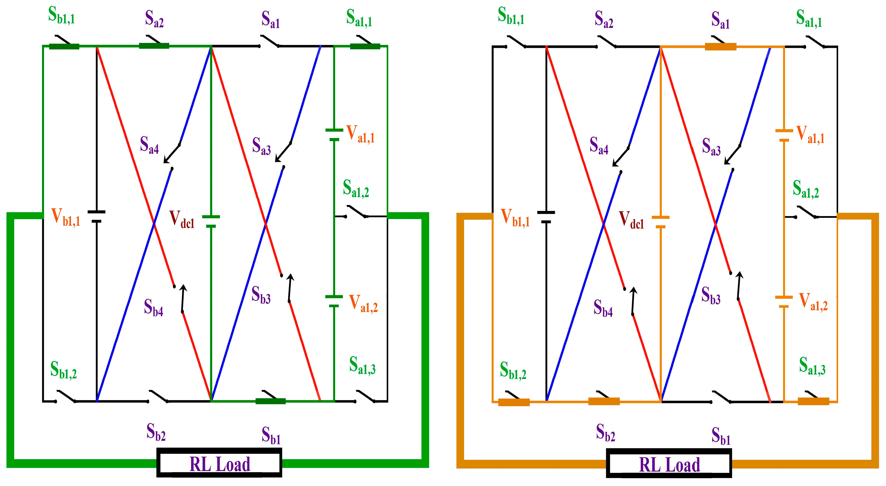
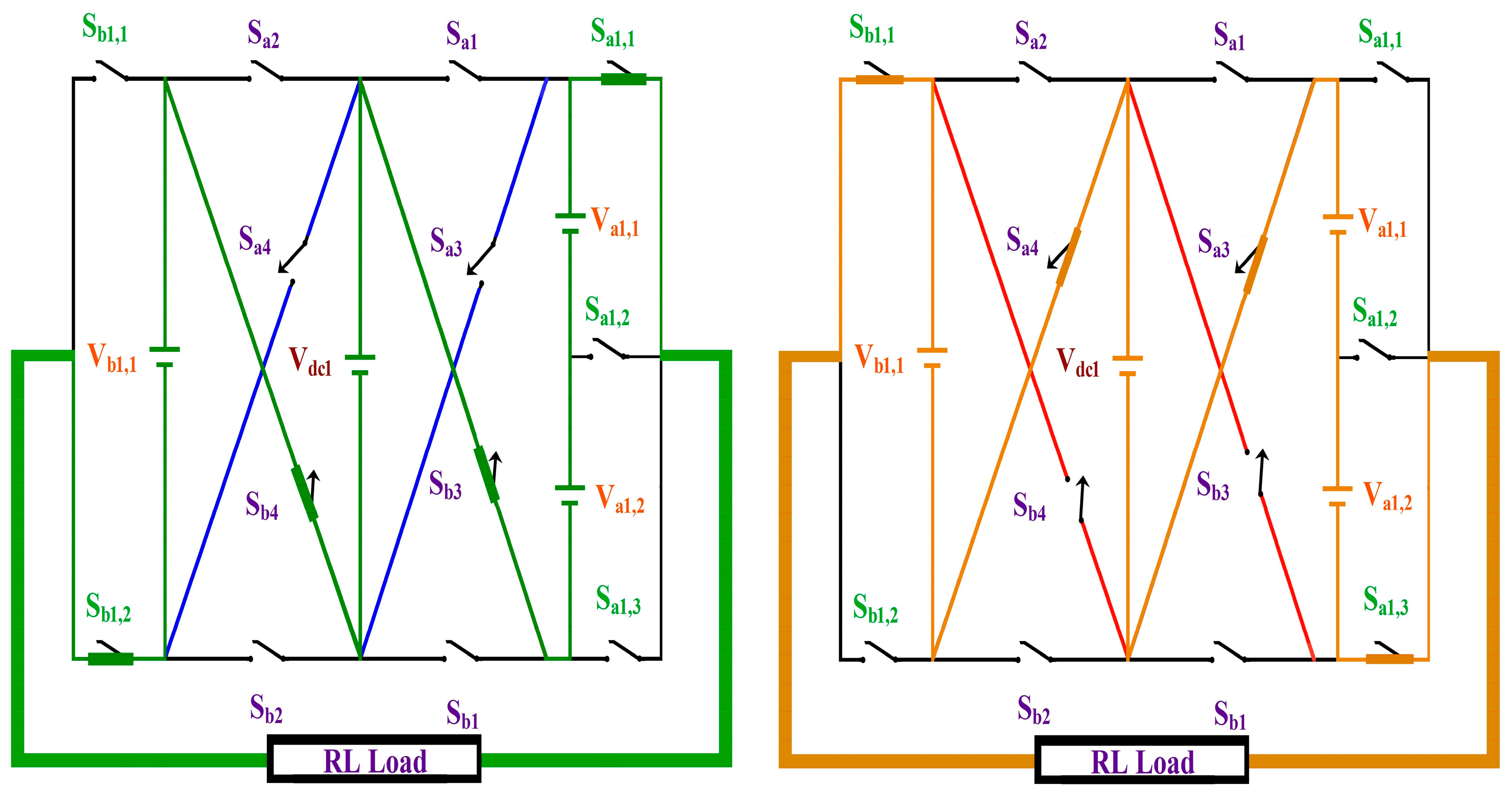
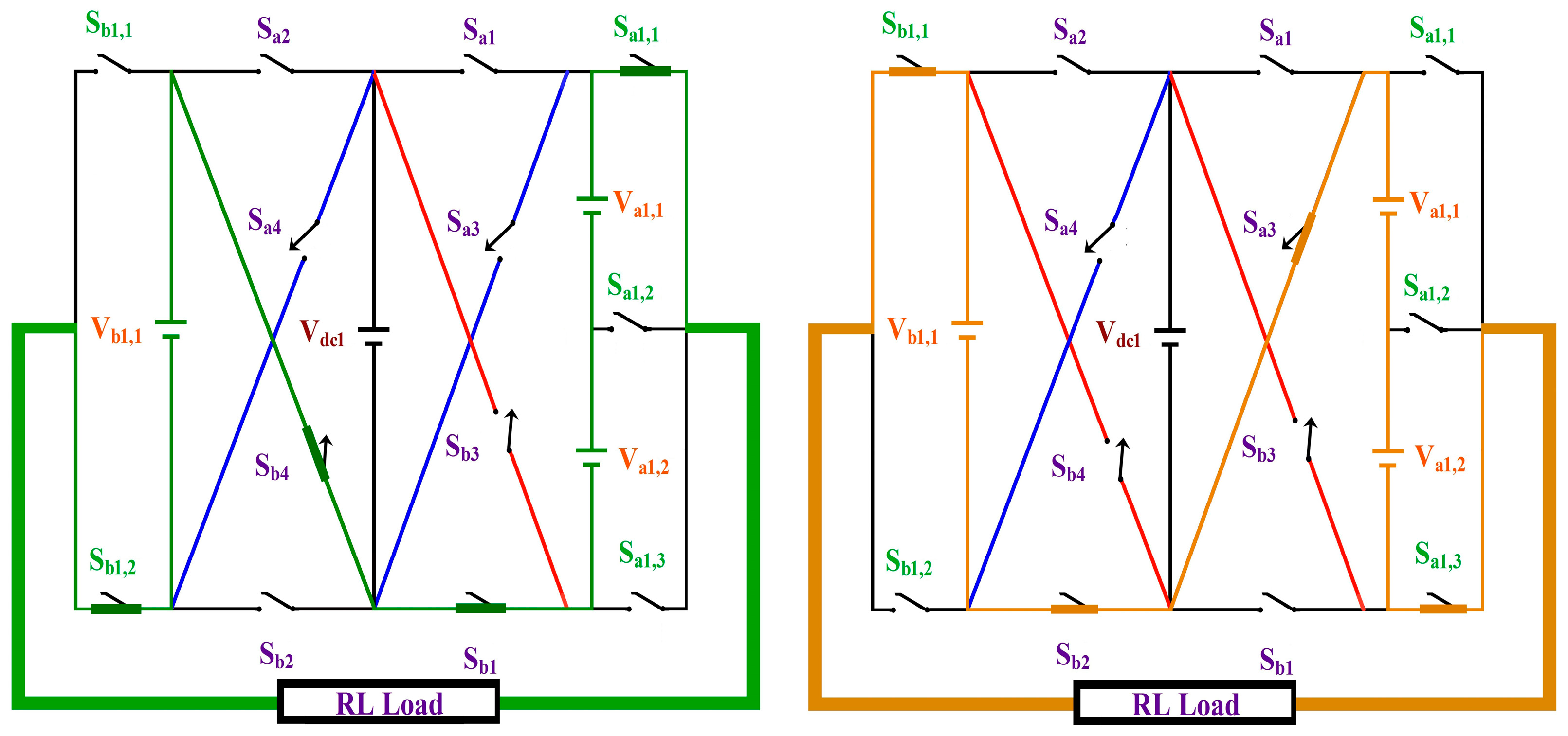
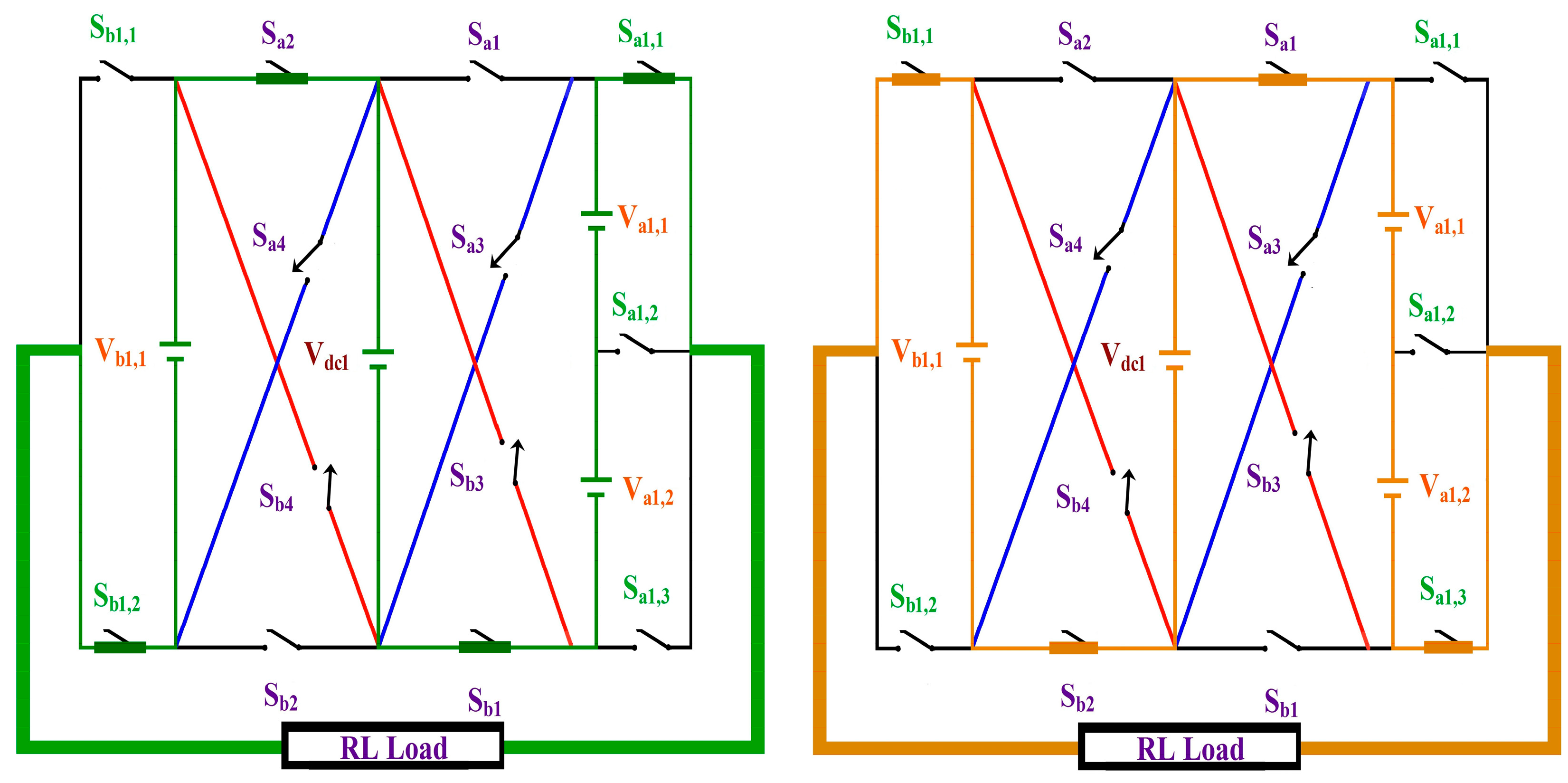
In a multilevel inverter, the number of switching devices and separated dc voltage sources are directly proportional to the output stair case waveform; this leads to the control circuit complexity, switching losses, and bulky size of the inverter. As a prominent solution to the above problem, modified novel crisscross augmented ladder topologies are portrayed in Figure 1. The suggested topology has the benefits of a lesser conducting path, which suggests a solution for circuit complexity and is well suited to operate in both binary and ternary voltage ratios. The crisscross ladder structure is formulated with an option of flexible and extendable in row and column wise, the separated dc sources (SDC’s) are connected in the cross links. The cross linked SDCs are enabled to perform additive and subtractive with crisscross to generate the intermediate levels. The SDCs are placed in columns, while the power switches are placed in rows. The first column consists of (Vb1,1, Vb1,2, Vb1,n),the second column is connected, and in between the structure consists of a nuance voltage Vdc,1 and extendable Vdc,n. The last column consists of (Va1,1, Va1,2, Va1,n). The upper segments switches (Sa1,1, Sa1, Sa2, Sb1,1) are constant and the lower segment switches(Sa1,+n, Sb1, Sb2, Sb1,+n) are extendable. The intermediate cross section switches are (Sa3, Sa4, Sb3, Sb4). The various operation modes are shown in Figure 2, Figure 3, Figure 4, Figure 5, Figure 6, Figure 7, Figure 8, Figure 9, Figure 10 and Figure 11. The clue to understanding the various operating modes, such as Figure 3 operating mode V ± 2 (Vb1,1-Vdc,1) and −(Va1,1-Vdc,1),is that the positive side conducting switches are colored in green while the negative cycle conducting switches are colored in brown, the cross connecting switches are colored in red and blue, and the pink colored areas in the row and column can be an expandable portion, as shown in schematic diagram 1.
In a similar way, all the other operating modes work as shown in Figure 2, Figure 3, Figure 4, Figure 5, Figure 6, Figure 7, Figure 8, Figure 9, Figure 10 and Figure 11. The suggested skeleton works in both symmetric and asymmetric voltage ratio, and is capable of producing various stair case voltage. The topology is undergone with symmetric voltage ratio (1:1:1:1), keeping all SDCs the same (Va1,1, Va1,2, Vdc1, Vb1,1 = 75 Volts), which results ((2 × n) + 1), i.e., 9 levels. The asymmetric voltage ratio with binary values (1:2:2:2) (Va1,1 = 43 Volts, Va1,2, Vdc1, Vb1,1 = 86 Volts) produces ((4 × n) − 1), i.e., 15 levels, with ternary voltage ratio (1:3:3:3); (Va1,1 = 30 Volts, Va1,2, Vdc1, Vb1,1 = 90 Volts) produces ((6 × n) − 3), i.e., 21 levels. The switching pattern for the 21 level is tabulated in Table 1.
Table 2 compares the number of devices which are required for the proposed and other topologies; it is evident that the proposed topologies use a lower number of devices in all conduction paths.

3. Modulation and Control Strategy

The multicarrier pulse width method (MCPWM) and fuzzy logic controller are used for the proposed topology, with a simple switching control algorithm technique. The control of complex nonlinear systems with knowledge based fuzzy logic controller is adopted here to reduce the total harmonic distortion in the output stair case waveform. FLC uses common mode harmonic approach strategy, focusing the corrections of deviation in active conduction path in the circuit. Three different voltage magnitude robust algorithms are suggested to demonstrate the feasibility of the proposed topology. The steps for the FLC interfacing diagram is shown in Figure 12. Seven fuzzy subsets are used to assign the membership function values to the linguistic variables: negative big (nb), negative medium (nm), negative small (ns), zero (zr), positive small (ps), positive medium (pm), and positive big (pb). The input variables are chosen to be variable e and ∆e, where e represents the error and ∆e is the change in error. The reference signal for the PWM generator is the output variable. For each of these processes, triangular membership functions have been chosen. Table 3 provides fuzzy associative memory for the suggested system. Table 4 explores the voltage magnitude of the proposed topology, expressing “m” as a function of “k”.
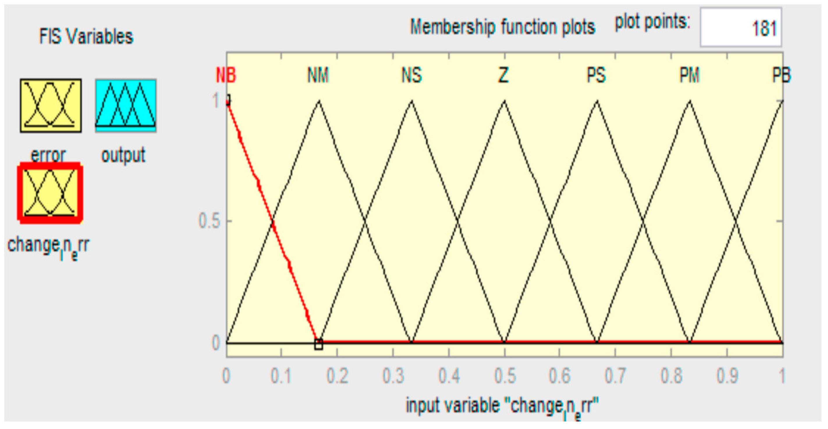
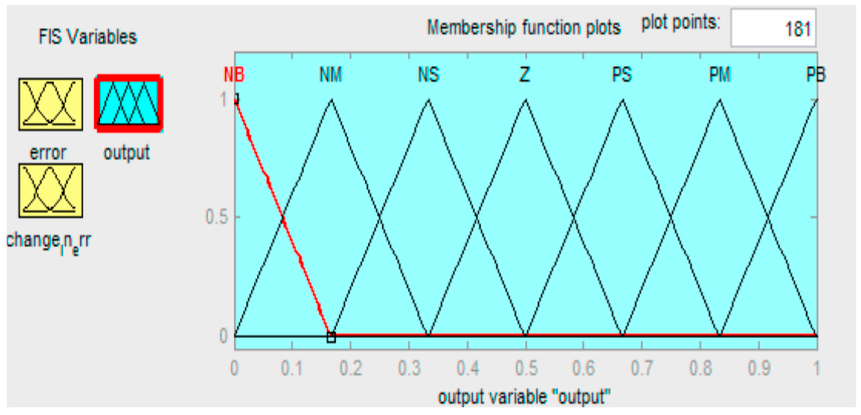
The FLC starts with the fuzzification, fuzzy inference and defuzzification. Initially the input parameter values are applied to fuzzification, the result obtained from the fuzzy vectors as membership functions, such as error, change of error, and output, are shown in Figure 13, Figure 14 and Figure 15. The fuzzy structures are analyzed with the help of 3D figure with respect to error, and change in error, and output, as shown in Figure 16, and the fuzzy rule is shown in Figure 17.

4. Simulation and Experimental Investigations

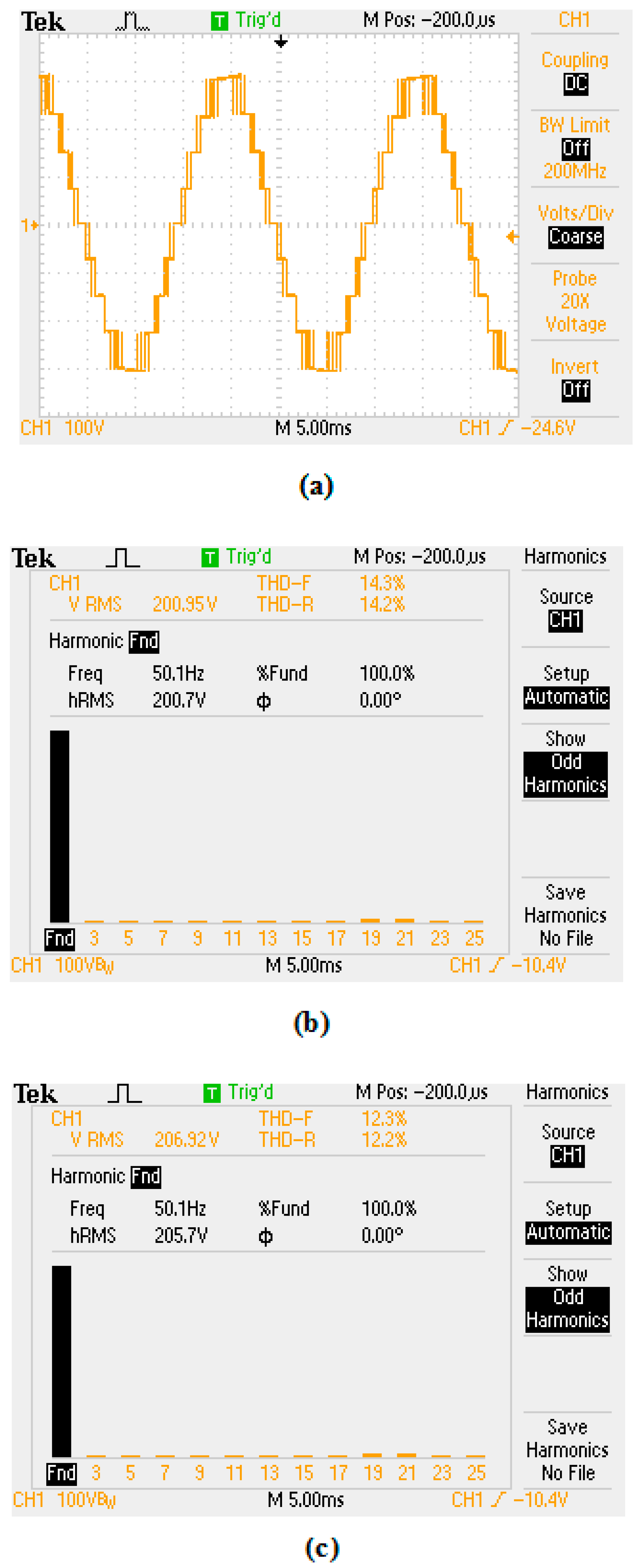
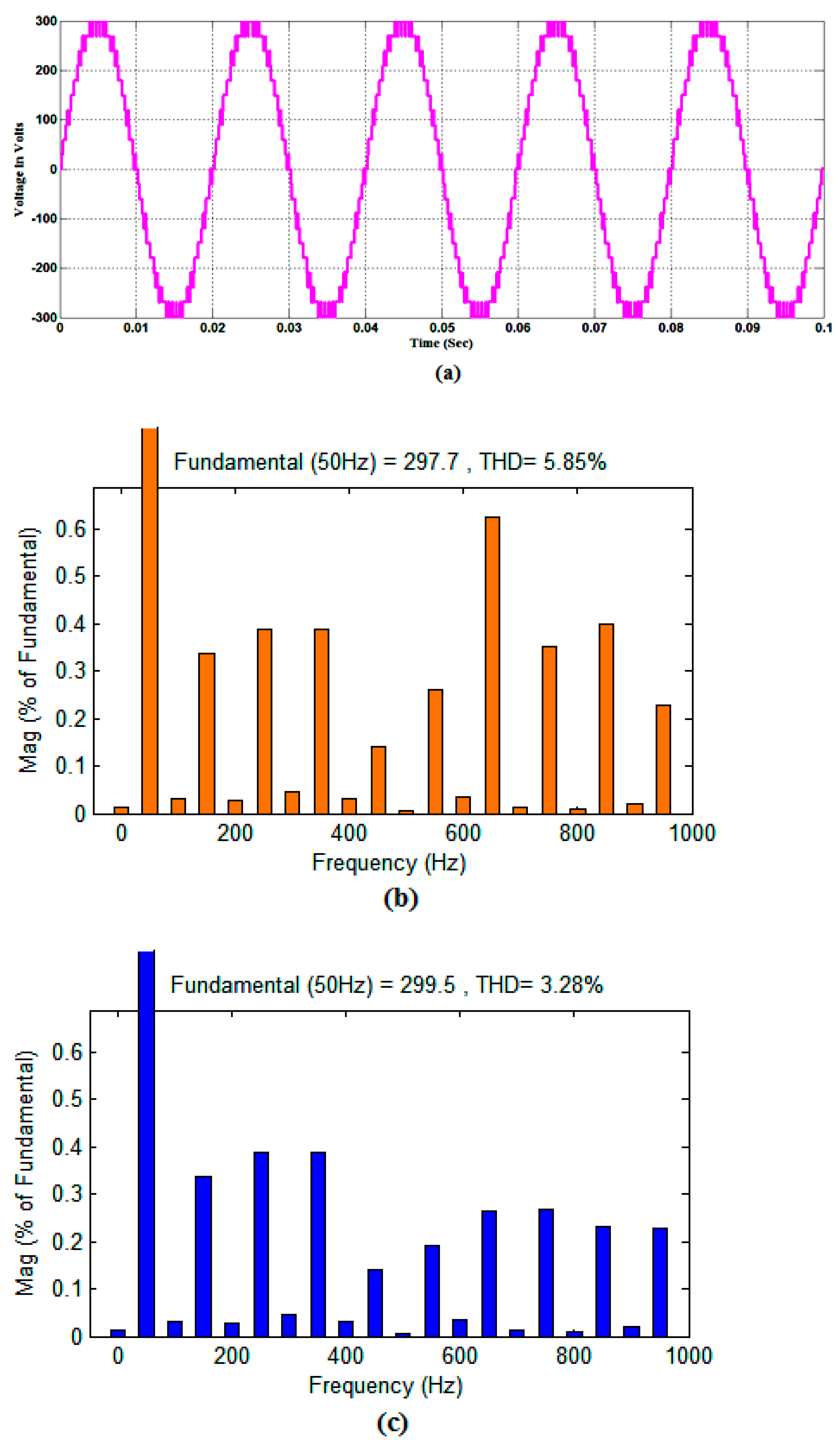
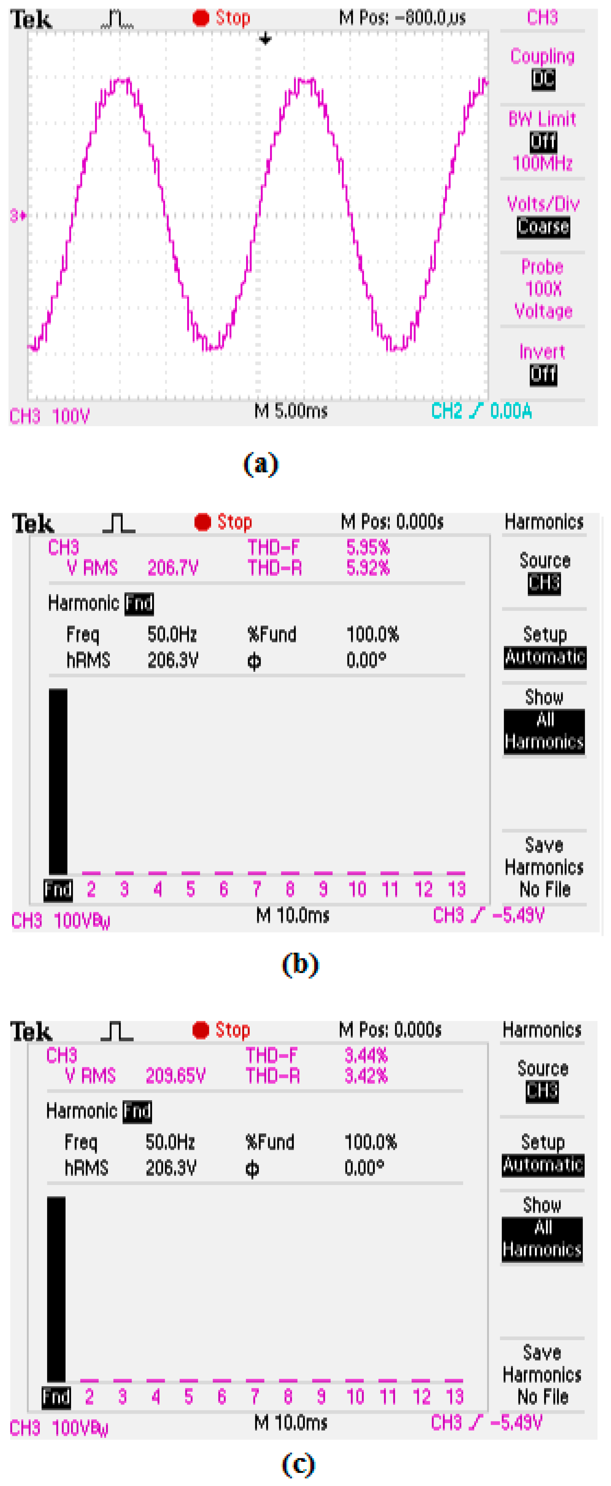
This section presents the simulation study, followed by experimental investigations which are clearly presented to validate the proposed CCAL multilevel inverter. Matlab R2017a is used for the simulation tool, and hardware proof of concept is implemented on Xilinx Spartan XC3SD1800A-FG676-4 Spartan 3A flat form. The proposed CCAL multilevel inverter utilizes four voltage sources and thirteen switches, although only four switches will be conducting in all modes of operation. This is the original contribution of research. A clear worth full comparison is made, with MCPWM scheme and FL controller scheme presented in Table 4 and Table 5. The simulation parameters for symmetric voltage ratio of 1:1:1:1 are as follows: keeping all SDCs the same, Va1,1, Va1,2, Vdc,1 and Vb1,1 = 75 Volts, with load resistance of R = 180 Ω and L = 120 mH, and switching frequency of 2 kHz, results in ((2 × n) + 1), i.e., 9 level. The simulated result is presented in Figure 18, with total harmonic distortion and laboratory proof of concept presented in Figure 19. The system undergoes asymmetric voltage ratio with binary values 1:2:2:2,Va1,1 = 43 Volts, Va1,2, Vdc,1, Vb1,1 = 86 Volts produces ((4 × n) − 1), 15 levels. The simulated result is presented in Figure 20, with total harmonic distortion and laboratory proof of concept presented in Figure 21. When the system undergoes ternary voltage ratio 1:3:3:3, Va1,1 = 30 Volts, Va1,2, Vdc,1, Vb1,1 = 90 Volts produces ((6 × n) − 3), 21 levels. The simulated result is presented in Figure 22, with total harmonic distortion and laboratory proof of concept presented in Figure 23. It is evident that the presented topology passes a lower number of conduction paths, compared in Table 6.
Table 5 shows the simulation results for the symmetric voltage ratio 1:1:1:1 keeping all the SDCs same as 75 V, secondly the asymmetric voltage ratio with binary ration of 1:2:2:2 as first SDCs 43 V and other SDCs as 86 V, and thirdly with ternary voltage ration 1:3:3:3 as first SDC 30 V and other SDCs 90 V. A clear comparison is made with and without fuzzy logic controller. The next Table 6 is the hardware result for the same voltage ratio. Table 7 compares the conduction path for the proposed and prevailing topologies.
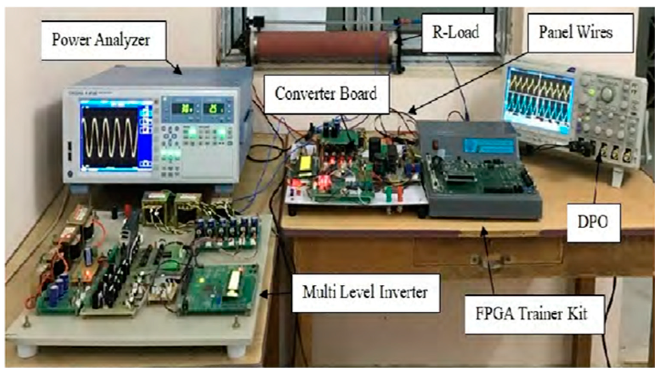
In this work, the proposed MLI has been suggested, with a view to decreasing the number of power components and conduction path when creating different staircase waveform. The proposed MLI has been tested in both symmetric/asymmetric modes, has been constituted for the CCAL MLI topology, and analyzed in simulation and experimental studies. The device count in CCAL MLI symmetric topology reduces, whereas the level increases during this way of operating. The requirement of a power device blocking voltage is the same as the compared CHBMLI topology, as shown in the comparison with similar topologies. The comparison in Table 7 suggests that the proposed topology uses less conduction path. The Hardware proof of concept is designed with Xilinx Spartan XC3SD1800A-FG676-4 Spartan 3A processor is portrayed in Figure 24.

5. Conclusions

A novel MLI topology is suggested (CCAL) which has the ability to work in symmetrical as well as asymmetrical modes. The presented structure has several benefits that include low switching stress, lower switching loss, and less dv/dt stress. Additionally, the planned methodology is compared with other topologies in terms of active power switches, passing diodes, coupling diodes, capacitors and a number of sources in Table 2. The reduction in THD is attained by employing the MCPWM technique with fuzzy logic controller in Table 5 and Table 6. Experimental investigations were performed to validate the results with simulation study. The result obtained was promising and fuzzy logic controller is found to be a good candidate to produce 21 levels of output, with low THD output and less conduction path, as reported in Table 7. For the three different voltage levels, only a small number of switches is utilized in the CCAL asymmetric topology without any increase in the blocking voltage. The CCAL topology with modularity in nature can be suggested for low and medium power application; ideally, it can be extended to electric vehicle applications.

Author Contributions

Conceptualization, Methodology, Supervision, S.S.; Formal analysis, Validation, K.C.; Writing, P.A. All authors have read and agreed to the published version of the manuscript.

Funding

This research received no external funding.

Institutional Review Board Statement

Not applicable.

Informed Consent Statement

Not applicable.

Data Availability Statement

Not applicable.

Conflicts of Interest

The authors declare no conflict of interest.

References

  1. Hota, A.; Jain, S.; Agarwal, V. An Improved Three Phase Five-level Inverter Topology with Reduced Number of Switching Power Devices. IEEE Trans. Ind. Electron. 2018, 65, 3296–3305. [Google Scholar] [CrossRef]
  2. Su, G.-J. Multilevel DC-Link Inverter. IEEE Trans. Ind. Appl. 2005, 41, 848–854. [Google Scholar] [CrossRef]
  3. Mondal, G.; Gopakumar, K.; Tekwani, P.N.; Levi, E. A Reduced-Switch-Count Five-Level Inverter with Common-Mode Voltage Elimination for an Open-End Winding Induction Motor Drive. IEEE Trans. Ind. Electron. 2007, 54, 2344–2351. [Google Scholar] [CrossRef]
  4. Ebrahimi, J.; Babaei, E.; Gharehpetian, G.B. A New Topology of Cascaded Multilevel Converters with Reduced Number of Components for High-Voltage Applications. IEEE Trans. Power Electron. 2011, 26, 3109–3118. [Google Scholar] [CrossRef]
  5. Nami, A.; Zare, F.; Ghosh, A.; Blaabjerg, F. A Hybrid Cascade Converter Topology with Series-Connected Symmetrical and Asymmetrical Diode-Clamped H-Bridge Cells. IEEE Trans. Power Electron. 2011, 26, 51–65. [Google Scholar] [CrossRef] [Green Version]
  6. Ramkumar, S.; Kamaraj, V.; Thamizharasan, S.; Jeevananthan, S. A new series parallel switched multilevel dc-link inverter topology. Int. J. Electr. Power Energy Syst. 2012, 36, 93–99. [Google Scholar] [CrossRef]
  7. Gupta, K.K.; Jain, S. Topology for multilevel inverters to attain maximum number of levels from given DC sources. IET Power Electron. 2012, 5, 435–446. [Google Scholar] [CrossRef]
  8. Babaei, E.; Kangarlu, M.F.; Mazgar, F.N. Symmetric and asymmetric multilevel inverter topologies with reduced switching devices. Electr. Power Syst. Res. 2012, 86, 122–130. [Google Scholar] [CrossRef]
  9. Lu, X.; Ge, B.; Peng, F.Z. Minimizing DC Capacitance Requirement of Cascadeded H-Bridge Multilevel Inverters for Photovoltaic Systems by 3rd Harmonic Injection. In Proceedings of the 2012 Twenty-Seventh Annual IEEE Applied Power Electronics Conference and Exposition (APEC), Orlando, FL, USA, 5–9 February 2012; pp. 240–245. [Google Scholar] [CrossRef]
  10. Ajami, A.; Oskuee, M.R.J.; Khosroshahi, M.T.; Mokhberdoran, A. Cascade-multi-cell multilevel converter with reduced number of switches. IET Power Electron. 2014, 7, 552–555. [Google Scholar] [CrossRef]
  11. Gupta, K.K.; Ranjan, A.; Bhatnagar, P.; Sahu, L.K.; Jain, S. Multilevel Inverter Topologies with Reduced Device Count: A Review. IEEE Trans. Power Electron. 2016, 31, 135–151. [Google Scholar] [CrossRef]
  12. Roy, T.; Sadhu, P.K.; Dasgupta, A. Cross-Switched Multilevel Inverter using Novel Switched Capacitor Converters. IEEE Trans. Ind. Electron. 2019, 66, 8521–8532. [Google Scholar] [CrossRef]
  13. Arun, N.; Noel, M.M. Crisscross switched multilevel inverter using cascaded semi-half-bridge cells. IET Power Electron. 2018, 11, 23–32. [Google Scholar] [CrossRef] [Green Version]
  14. Farhadi-Kangarlu, M.; Torshakaan, M.B.; Neyshabouri, Y. A Transformerless DSTATCOM Based on Cross-Switched Multilevel Inverter for Grid Voltage Regulation. Int. J. Electr. Eng. Inform. 2020, 12, 398–417. [Google Scholar]
  15. Kangarlu, M.F.; Babaei, E. Cross-switched multilevel inverter: An innovative Topology. IET Power Electron. 2013, 6, 642–651. [Google Scholar] [CrossRef]
  16. Khosroshahi, M.T. Crisscross cascade multilevel inverter with reduction in number of components. IET Power Electron. 2014, 7, 2914–2924. [Google Scholar] [CrossRef]
  17. Titus, S. A Stipulation Based Sources Insertion Multilevel Inverter (SBSIMLI) for Waning the Component Count and Separate DC Sources. J. Electr. Eng. Technol. 2017, 12, 1519–1528. [Google Scholar]
  18. Kannan, C.; Mohanty, N.K.; Selvarasu, R. A new topology for cascaded H-bridge multilevel inverter with PI and Fuzzy control. Energy Procedia 2017, 117, 917–926. [Google Scholar] [CrossRef]
  19. Samadaei, E.; Gholamian, S.A.; Sheikholeslami, A.; Adabi, J. An envelope type (E-Type) module: Asymmetric multilevel inverters with rreduced components. IEEE Trans. Ind. Electron. 2016, 63, 7148–7156. [Google Scholar] [CrossRef]
  20. Jose, S.E.; Titus, S. A Level Dependent Source Concoction Multilevel Inverter Topology with a Reduced Number of Power Switches. J. Power Electron. 2016, 16, 1316–1323. [Google Scholar] [CrossRef] [Green Version]
  21. Khosroshahi, M.T.; Ajami, A.; Mokhberdoran, A.O.; OsKuee, M.J. Multilevel hybrid cascade-stack inverter with substantial reduction in switches number and power losses. Turk. J. Electr. Eng. Comput. Sci. 2015, 23, 987–1000. [Google Scholar] [CrossRef]
  22. Dhanamjayulu, C.; Prasad, D.; Padmanaban, S.; Maroti, P.K.; Holm-Nielsen, J.B.; Blaabjerg, F. Design and Implementation of Seventeen Level Inverter with Reduced Components. IEEE Access 2021, 9, 16746–16760. [Google Scholar] [CrossRef]
  23. Siddique, M.D.; Mekhilef, S.; Rawa, M.; Wahyudie, A.; Chokaev, B.; Salamov, I. Extended Multilevel Inverter Topology with Reduced switch Count and Voltage stress. IEEE Access 2020, 8, 201835–201846. [Google Scholar] [CrossRef]
  24. Arif, M.S.B.; Mustafa, U.; Ayob, S.B.M.; Rodriguez, J.; Nadeem, A.; Abdelrahem, M. Asymmetrical 17-Level Inverter Topology with Reduced Total Standing Voltage and Device Count. IEEE Access 2021, 9, 69710–69723. [Google Scholar] [CrossRef]
  25. Siddique, M.D.; Iqbal, A.; Memon, M.A.; Mekhilef, S. A New Configurable Topology for Multilevel Inverter with Reduced Switching Components. IEEE Access 2020, 8, 188726–188741. [Google Scholar] [CrossRef]
  26. Zolfaghar, M.; Najafi, E.; Hasanzadeh, S. A modified diode clamped inverter with reduced number of switches. In Proceedings of the 2018 9th Annual Power Electronics, Drives Systems and Technologies Conference (PEDSTC), Tehran, Iran, 13–15 February 2018; pp. 53–58. [Google Scholar]
  27. Bouafassa, A.; Rahmani, L.; Kessal, A.; Babes, B. Unity power factor Converter based on a Fuzzy controller and Predictive Input Current. ISA Trans. 2014, 53, 1817–1821. [Google Scholar] [CrossRef]
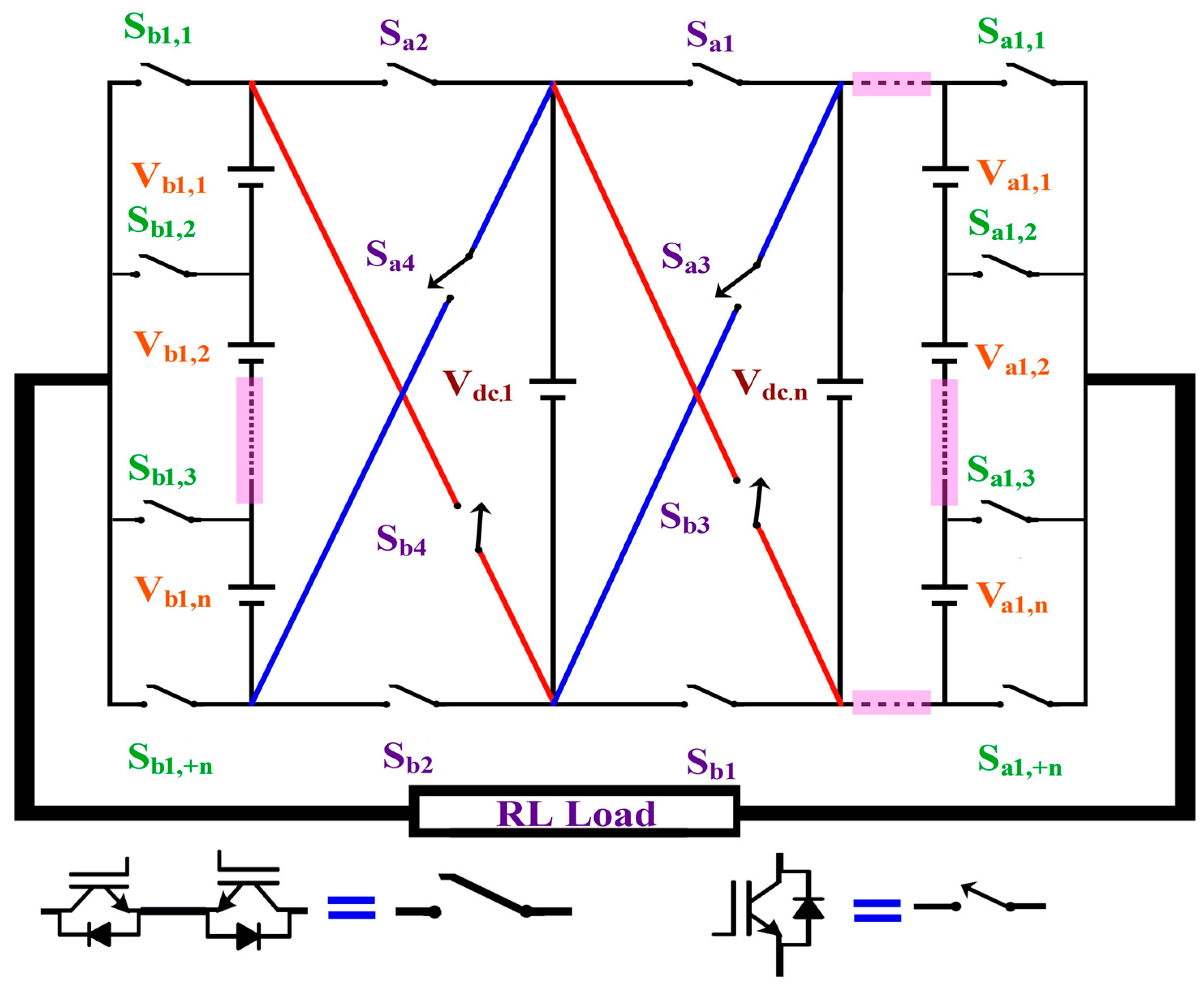
Figure 1. Schematic Structure of CCAL.
Symmetry 15 01366 g001
Figure 2. Mode of operating level 1.
Symmetry 15 01366 g002
Figure 3. Mode of operating level 2.
Symmetry 15 01366 g003
Figure 4. Mode of operating level 3.
Symmetry 15 01366 g004
Figure 5. Mode of operating level 4.
Symmetry 15 01366 g005
Figure 6. Mode of operating level 5.
Symmetry 15 01366 g006
Figure 7. Mode of operating level 6.
Symmetry 15 01366 g007
Figure 8. Mode of operating level 7.
Symmetry 15 01366 g008
Figure 9. Mode of operating level 8.
Symmetry 15 01366 g009
Figure 10. Mode of operating level 9.
Symmetry 15 01366 g010
Figure 11. Mode of operating level 10.
Symmetry 15 01366 g011
Figure 12. Steps for fuzzy interfacing, fuzzification, fuzzy inference and defuzzification.
Symmetry 15 01366 g012
Figure 13. Plot of error membership function.
Symmetry 15 01366 g013
Figure 14. Plot of change in error membership function.
Symmetry 15 01366 g014
Figure 15. Plot of output membership function.
Symmetry 15 01366 g015
Figure 16. Fuzzy structure.
Symmetry 15 01366 g016
Figure 17. Fuzzy rules.
Symmetry 15 01366 g017
Figure 18. (a) CCAL multilevel inverter simulated output voltage 9 level. (b)Harmonic Spectrum, THD without FLC 12.85%. (c) Harmonic Spectrum, THD with FLC 9.28%.
Symmetry 15 01366 g018
Figure 19. (a) CCAL multilevel inverter experimental output voltage 9 level. (b) Harmonic Spectrum, THD without FLC 14.3%. (c) Harmonic Spectrum, THD with FLC 12.3%.
Symmetry 15 01366 g019
Figure 20. (a) CCAL Multilevel inverter simulated output voltage and 15 level. (b) Harmonic Spectrum, THD without FLC 8.34%. (c) Harmonic Spectrum, without FLC 8.34%. (c) THD with FLC 7.14%.
Symmetry 15 01366 g020
Figure 21. (a) CCAL Multilevel inverter experimental output voltage 15 level. (b) Harmonic Spectrum THD without FLC 9.5%. (c) Harmonic Spectrum, THD with FLC 8.1%.
Symmetry 15 01366 g021
Figure 22. (a) CCAL multilevel inverter simulated output voltage 21 level. (b) Harmonic Spectrum, THD without FLC 5.85%. (c) Harmonic Spectrum, THD with FLC 3.28%.
Symmetry 15 01366 g022
Figure 23. (a) CCAL multilevel inverter experimental output voltage of 21 level. (b) Harmonic Spectrum, THD without FLC 5.95%. (c) Harmonic Spectrum, THD with FLC 3.44%.
Symmetry 15 01366 g023
Figure 24. Hardware proof of concept Xilinx Spartan XC3SD1800A-FG676-4 Spartan 3A.
Symmetry 15 01366 g024
Table 1. CCAL switching pattern for 21 level with ternary voltage ratio (1:3:3:3).
SDCsConducting Switches ‘m’ Level Conducting Switches SDCs
Va1,1 + Va1,2 + Vb1,1 + Vdc1Sb1, Sa1,1, Sb1,2, Sa2+10−10Sa1, Sa1,3, Sb1,1, Sb2−(Va1,1 + Va1,2 + Vb1,1 + Vdc,1)
Va1,1 + Va1,2 + Vb1,1Sb1, Sa1,1, Sb1,2, Sb4+9−9Sa3, Sa1,3, Sb1,1, Sb2−(Va1,1 + Va1,2 + Vb1,1)
Va1,1 + Va1,2 + Vb1,1 − Vdc,1Sb4, Sa1,1, Sb1,2, Sb3+8−8Sa4, Sa1,3, Sb1,1, Sa3−(Va1,1 + Va1,2 + Vb1,1 − Vdc,1)
Va1,1 + Va1,2 + Vdc,1Sb1, Sa1,1, Sb1,1, Sa2+7−7Sa1, Sa1,3, Sb1,2, Sb2−(Va1,1 + Va1,2 + Vdc,1)
Va1,1 + Va1,2Sb1, Sa1,1, Sb1,2, Sb2+6−6Sa1, Sb1,1, Sa1,3, Sa2−(Va1,1 + Va1,2)
Va1,2 + Vb1,1 − Vdc,1Sb4, Sa1,2, Sb1,2, Sb3+5−5Sb1,1, Sa4, Sb1, Sa1,2−(Va1,2 + Vb1,1 − Vdc,1)
Vb1,1 + Vdc,1Sb1, Sa1,3, Sb1,2, Sa2+4−4Sb2, Sa1,1, Sb1,1, Sa1−(Vb1,1 + Vdc,1)
Vb1,1Sa2, Sa1,1, Sb1,2, Sa1+3−3Sb2, Sb1,1, Sa1,3, Sb1−Vb1,1
Vb1,1 − Vdc,1Sb4, Sa1,1, Sb1,2, Sa1+2−2Sa3, Sa1,2, Sb1,1, Sa2−(Va1,1-Vdc,1)
Vdc,1Sb1, Sa1,3, Sb1,1, Sa2+1−1Sa1, Sa1,1, Sb1,2, Sb2−Vdc,1
Sa1, Sa1,1, Sb1,1, Sa20Sa1, Sa1,1, Sb1,1, Sa2
Table 2. Comparison between the CCAL MLI and other prevailing topologies “m” stair case level.
MLI StructureCascaded H Bridge MLI StructureDiode Clamped MLI Structure Capacitor Clamped MLI StructureProposed Crisscross MLI Structure
Active power Switches2(m − 1)2(m − 1)2(m − 1)(m + 17)/2
Passing diodes -
Coupling diodes 2(m − 3)
Voltage splitting capacitors (m − 1)/2(m − 1)/2
Coupling capacitors (2m − 6)/2
Number of sources(m − 1)/211(m − 1)/2
Table 3. Fuzzy associate memory for the proposed system.
e∆e
nbnmnszrpspmpb
nbnbnbnbnmnmnszr
nmnbnbnmnmnszrps
nsnbnmnmnszrpspm
zrnmnmnszrpspmpm
psnmnszrpspmpmpb
pmnszrpspmpmpbpb
pbzrpspmpmpbpbpb
Table 4. Voltage magnitude algorithm expressing “m” as a function of “k”.
FLC
Algorithm
Voltage Source
Magnitude
Vmax‘m’
Algorithm 1 V 1 , o = V 1 , 1 = V 1 , 2 = V dc
V j , 0 = V j , 1 = V j , 2 = 6 k 1 V dc
j = 2, 3, …, k
3 + 3 j = 2 k 6 j 1 Vdc 2 3 + 3 j = 2 k 6 j 1 + 1
Algorithm 2 V 1 , o = V 1 , 1 = V 1 , 2 = V dc
V j , 0 = V j , 1 = V j , 2 = 7 k 1 V dc
j = 2, 3, …, k
3 + 3 j = 2 k 7 j 1 Vdc 2 3 + 3 j = 2 k 7 j 1 + 1
Algorithm 3 V 1 , o = V 1 , 1 = V 1 , 2 = 7 k 1 V dc
V j , 0 = V j , 1 = V j , 2 = 2 × 7 k 1 V dc
j = 2, 3, …, k
5 + 5 j = 2 k 7 j 1 Vdc 2 5 + 5 j = 2 k 7 j 1 + 1
Table 5. Simulated result comparison with and without fuzzy logic controller.
Operating Mode Simulated Result Voltage
Levels
VoltageCurrentFundamental RMSVoltage
THD
Current
THD
Symmetric voltage ratio (1:1:1:1)Without FLC295.73.14209.0912.85%3.45%9
With FLC298.52.98211.079.28%3.15%
Asymmetric voltage ratio Binary (1:2:2:2)Without FLC296.42.94209.588.34%3.03%15
With FLC298.52.98211.077.14%2.58%
Asymmetric voltage ratio Ternary (1:3:3:3)Without FLC297.73.04210.055.85%3.35%21
With FLC299.52.86211.773.28%2.35%
Table 6. Hardware result comparison with and without fuzzy logic controller.
Operating Mode Hardware Result Voltage
Levels
VoltageCurrentFundamental RMSVoltage
THD
Current
THD
Symmetric voltage ratio (1:1:1:1)Without FLC284.23.14200.9514.38%3.05%9
With FLC292.52.98206.9212.58%2.95%
Asymmetric voltage ratio Binary (1:2:2:2)Without FLC289.32.94204.599.64%3.13%15
With FLC294.52.98208.248.14%3.08%
Asymmetric voltage ratio Ternary (1:3:3:3)Without FLC291.73.04206.265.95%3.05%21
With FLC296.52.86209.653.44%2.25%
Table 7. Comparison of the conduction path in the prevailing multilevel inverter topology and the proposed CCAL multilevel inverter.
Voltage LevelsCascaded H Bridge MLIDiode Clamped MLIFlying Capacitor MLICHB-MLDCLIDC-
MLDCLI
CC-
MLDCLI
Proposed CCAL MLI
98886664
151414149994
212020201212124
Disclaimer/Publisher’s Note: The statements, opinions and data contained in all publications are solely those of the individual author(s) and contributor(s) and not of MDPI and/or the editor(s). MDPI and/or the editor(s) disclaim responsibility for any injury to people or property resulting from any ideas, methods, instructions or products referred to in the content.