1. Introduction
Optical logic components have attracted considerable attention due to their strong capability in the optical communication field and potential to support computing techniques for the future improvement of signal processing in all-optical data networks [
1,
2,
3,
4].
All-optical logic components can be used in networking applications [
5,
6,
7,
8], such as optical computing, addressing, signal regeneration, clock recovery, and error detection.
For the optimal design of complex logic components, compact, fast, and low-power logic gates are essential.
A variety of materials and technologies have been used to design all-optical logic gates, including waveguide interferometers, optical fibers [
9,
10,
11,
12], semiconductor optical amplifiers [
13,
14,
15,
16,
17,
18], and photonic crystals (PC) [
19,
20,
21,
22,
23,
24,
25]. The above-mentioned materials and technologies have certain fundamental limitations, such as big size, low speed, and difficulty in performing chip-scale integration, that cannot be worked around.
In particular, fiber-based logic gates have physical limitations that prevent them from being integrated at the chip scale. Semiconductor optical amplifiers are limited by their inevitable spontaneous emission noise, whereas PCs can ensure a solution to all the above limitations since they can provide logic gates with a simple structure, ultra-compact size, low power loss, and high speed. A PC square is a periodic dielectric nanostructure with different reflective indexes that affect the propagation of electromagnetic waves in the structure.
Some research has focused on the development and optimization of PC logic gates. Several of these works are based on nonlinear optical effects [
26], the self-collimation effect [
27], multi-mode interferometers [
28], PC ring resonators (RR) [
29], and the Y-shaped PC waveguide [
30]. To the best of our knowledge, no optical half-adder (HA), constructed using optical logic gates based on cross-shaped PC waveguides combined with RR, has been proposed.
Some other HA structures have been proposed, such as a design that uses a two-dimensional PC made of silicon rods in air and four micro-RRs in the center [
31]; the basic structure of an all-optical HA is that of a two-dimensional PC that contains dielectric rods in the air with two circular RRs [
32]. The results of our proposed structure are compared to this recent research.
In this paper, a new structure for an optical HA without nonlinear materials is proposed. The proposed HA is built from a symmetrical configuration of all-optical AND and XOR logic gates that are based on cross-shaped PC waveguides. The AND gate consists of two 2D PC racetrack RRs, while the XOR gate consists of two 2D PC quasi-square RRs composed of cylindrical silicon (Si) rods in silica (SiO2) that share a full band gap.
Racetrack PC RRs [
33] are known for their high-quality factors and low insertion losses, and they have been used in a variety of applications such as optical filters, delay lines, and biosensors. On the other hand, quasi-square PC RRs [
34] are known for their strong light confinement, which leads to high-quality factors, and they have been used in applications such as lasers and nonlinear optics.
The proposed structure has potential application prospects in photonic integrated circuits. The electromagnetic wave propagation in the time domain of the logic gates was simulated using a two-dimensional finite-difference time domain (FDTD), and the photonic band gap (PBG) was calculated using the plane-wave expansion (PWE) method.
This paper has a strong relation to the concept of symmetry, which is a fundamental aspect of various scientific disciplines. In our case, we investigated the combination of optical physics for the future development of quantum computing application by designing a basic optical HA element as part of the photonic arithmetic logic unit.
2. Principle and Analysis
The PBG shows at which range of frequencies the wave propagating in the structure will be reflected by it; it is depicted in the band structure that can be obtained by using the PWE principle and Maxwell’s equations, corresponding to the transverse electric (TE) and transverse magnetic (TM) polarizations, to numerically solve the following equation:
where
H is the magnetic field,
r is the relative permittivity,
is the angular frequency, and
c is the speed of light. From the frequency range, we can calculate the range of wavelengths that should be used.
For analyzing the electromagnetic waves propagating in the optical paths, the FDTD method can be used. This method contributes a direct solution to the curl time-dependent Maxwell’s equation in nonmagnetic materials:
where
D is the displacement field,
H and
E are the magnetic and electric field,
is the angular frequency,
r and
0 are the relative permittivity and vacuum permittivity, and
0 is the vacuum permeability.
The FDTD method resolves the equations using a discrete spatial and temporal grid. Within the grid cell, each field component is resolved at a marginally different location on the grid. The collected data from the FDTD solver is typically automatically interpolated to the origin of each grid point, alleviating the need for the end user to address this matter in their analysis. The FDTD technique employs a rectangular, Cartesian mesh style wherein all key simulation parameters (such as material properties, geometrical information, electric and magnetic fields) are computed at every mesh point. While using a smaller mesh yields a more precise depiction of the device, it comes at a considerable expense. As the mesh size decreases, simulation time and memory demands tend to increase. However, the FDTD solver offers various functionalities, including the conformal mesh algorithm, that enables one to attain precise outcomes even when using a comparatively coarse mesh.
A PC RR consists of a ring-shaped waveguide that is constructed from a photonic crystal, with periodic modulations in the refractive index around the ring circumference. This periodicity creates a band gap in the transmission spectrum of the waveguide and results in the confinement and resonant enhancement of light at specific frequencies.
The proposed design consists of two racetrack PC RRs and two quasi-square PC RRs that construct an AND and XOR gate, respectively. The difference between a racetrack PC RR and a quasi-square PC RR lies in their geometries, which can affect their optical properties and potential applications.
Phase difference refers to the difference in the phase of the electric field between two points on the resonator that are separated by a certain distance. The phase difference is an important parameter in the operation of a PC RR because it determines the constructive or destructive interference of the light waves that circulate within the resonator.
To design the PC RR to work at a certain wavelength, an optimization needs to be performed to create the effective path length for the light waves as they travel across the ring, such that the phase difference at different points on the ring will correspond to our operating wavelength.
The phase difference in a PC RR can be controlled by adjusting the physical dimensions of the resonator, such as the radius or the periodicity of the photonic crystal. By optimizing the phase difference, the resonant frequencies of the PC RR can be tuned to achieve an operating wavelength of 1550 nm.
There is a tradeoff made, when choosing an RR, between the time it takes the light waves to travel through the RR, which directly affects the stabilization time, and the coupling efficiency of the light to the RR.
The time it takes the light to travel through the RR can be described by the expression
where
ng is the group index of the waveguide mode and
L is the waveguide length of the ring. For a racetrack RR, it is given by the following expression:
LR = 2(π
Rin +
dc). For a quasi-square RR, the equation is:
Ls = 2π
Rin, where
Rin is the inner radius and
dc is the straight sections of the racetrack RR. This means the racetrack RR will allow for a longer stabilization time but a better coupling effect, since its coupling distance is approximately the length of the straight sections
dc.
In this proposed structure, an optimization of both radii and the periodicity of the photonic crystal has been completed to achieve an operating wavelength of 1550 nm.
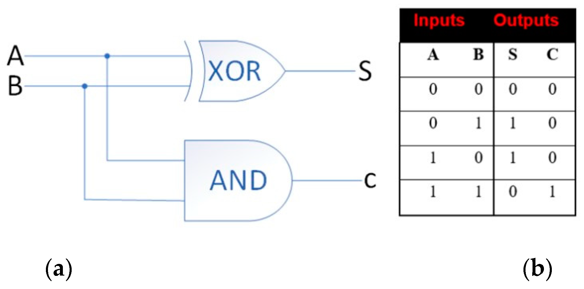
Generally, an HA consists of two logic gates, XOR and AND.
Figure 1 shows that the outputs of the HA sum (S) and carry out (C) are identical to the outputs of the two logic gates XOR and AND, respectively, for the respective inputs of A and B.
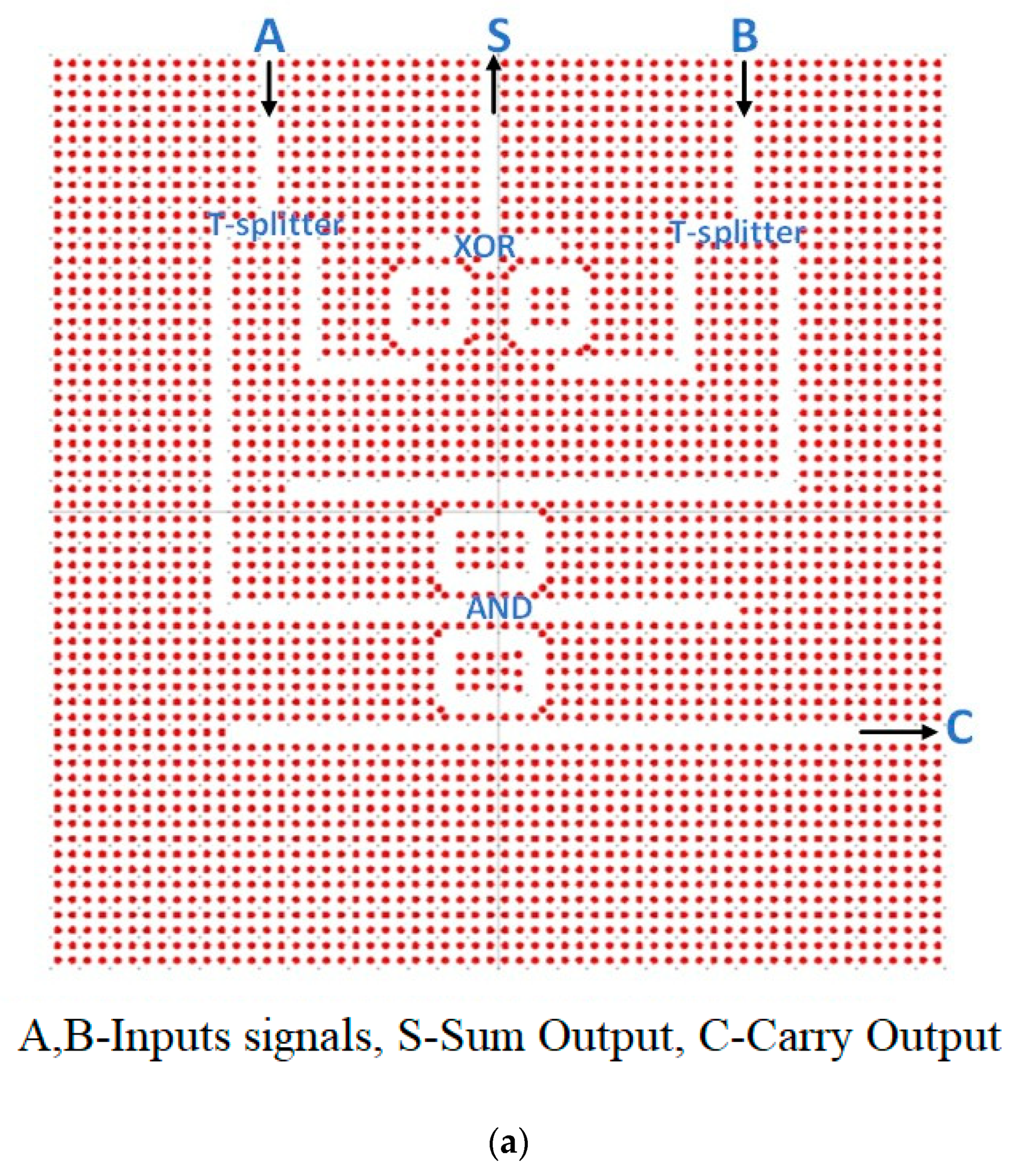
The optical logic HA structure is based on two T-splitters that split the wave with minimal power loss, XOR, and AND logic gates, as shown in
Figure 2a. In this figure, red color areas represent Si and white areas represent SiO
2. To simplify the complex optical HA shown in
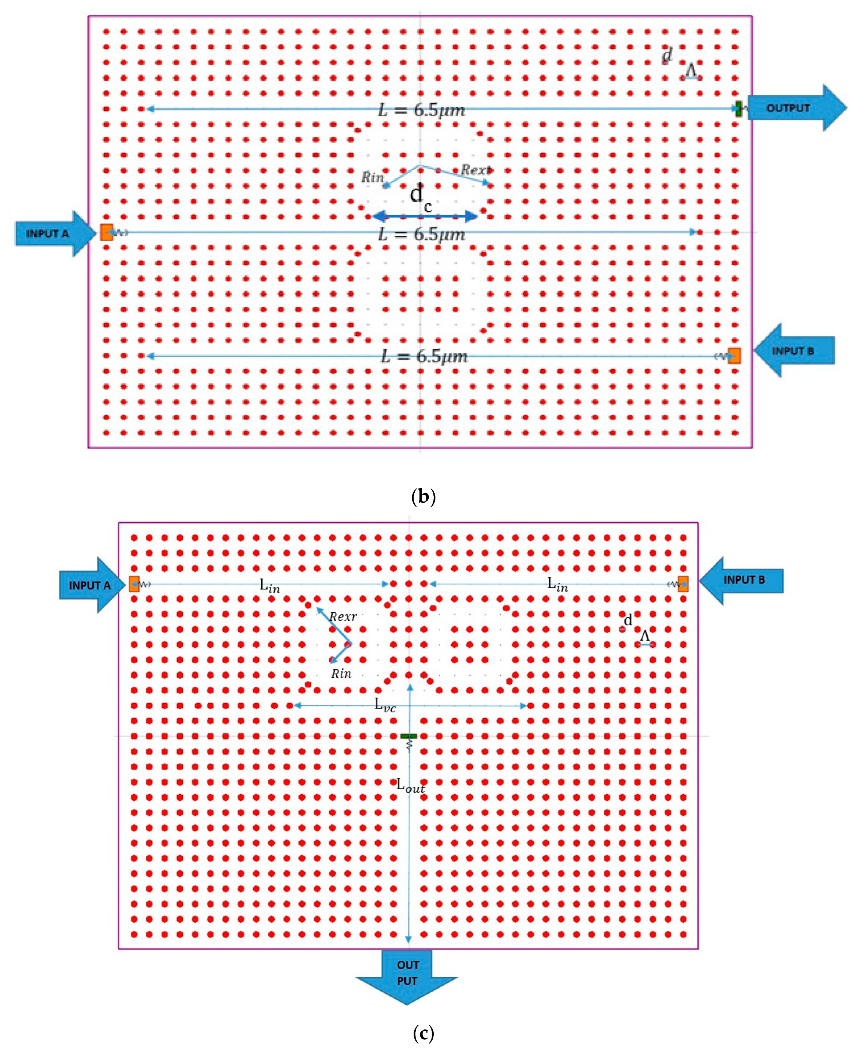
Figure 2a, two optical logic gates AND and XOR have been proposed separately with the same PC unit cell configuration and PC structure parameters.
Figure 2b illustrates the proposed design of an all-optical AND gate. It consists of three horizontal waveguides and two racetrack RRs. The length (L) of each waveguide is 6.5 µm. Both RRs have the same inner radius Rin of 0.6 µm and the same external radius Rext of 1.6 µm and are located between two waveguides. The first RR is located above input B, and the second RR is located above input A. The all-optical AND logic gate has two input ports and one output port.
Figure 2c illustrates the proposed design of an all-optical XOR gate. It comprises three horizontal waveguides, one vertical waveguide, and two quasi-square RRs. The length (Lin) of the two upper horizontal waveguides is 9 µm, and the third horizontal waveguide Lvc is 8 µm. The length (Lout) of the vertical waveguide is 6 µm. Both RRs have the same inner radius Rin of 0.5 µm and the same external radius Rext of 1.5 µm and are located under the input waveguides. The all-optical XOR logic gate has two input ports and one output port.
For both logic gates, the diameter (d) of each rod is 200 nm and the pitch (Λ) that represents the distance between two-rod centers is 500 nm and are shown in
Figure 2b,c.
The reason for using this special configuration in both logic gates is to ensure a full TE band gap with an orthogonal magnetic field to the rods.
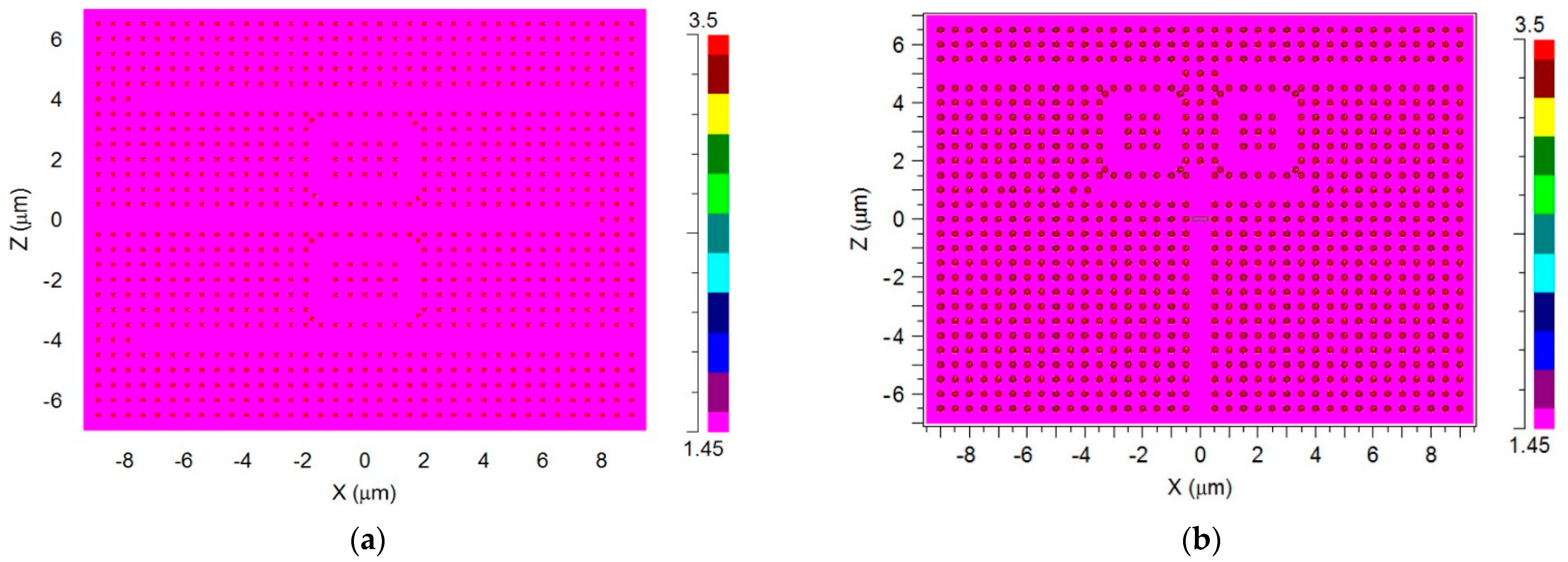
Figure 3a,b show the refractive index profile of the logic gates. In these figures, two-dimensional cylindrical Si rods are represented by a refractive index of 3.5, and the cover area and SiO
2 with a refractive index of n
SiO2 equal to 1.45 share a full band gap at a wavelength of 1550 nm.
The contrast ratio describes the distinction between logic 1 and logic 0 in a photonic device and is an essential parameter when designing optical logic components; it determines their effectiveness. The contrast ratio can be calculated by the following equation:
where
P1 and
P0 represent the light intensity value of the logic 1 and logic 0 state, respectively, at the output port of a logic gate.
The insertion loss (IL) is given by the following equation:
where
Pout is the power level at the output logic gate, and
Pin is the total input power for the two input sources.
3. Simulation Results
The simulation process and numerical optimization of the proposed all-optical logic gates XOR and AND were performed with Rsoft Photonics CAD Suite software (version 2021.03), which uses the Band-Solve tool calculation method based on the PWE principle for solving the PBG, whereas the Rsoft FULLWAVE tool, which uses the FDTD method, was applied for the simulation of the transmission diagram and reflection of optical power in the logic gates’ output.
The AND and XOR optical logic gates receive a Gaussian pulse at the input, which was used as an input signal in the simulations.
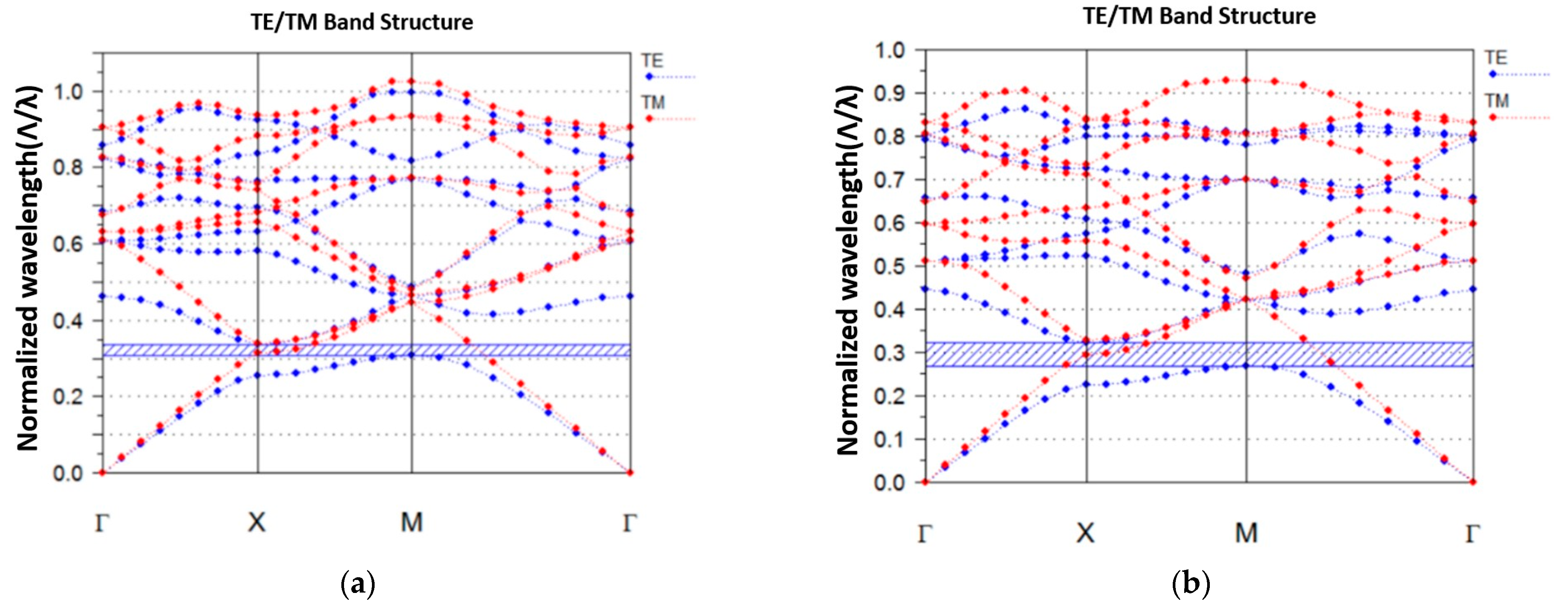
For locating and optimizing the PBG and calculating the dispersion of defected states, testing only one small group of points in the first Brillouin zone (1BZ) was sufficient. A group of symmetrical points characterizes every crystalline structure, and to build a graph that describes the PBG, it was essential to determine the points of symmetry in 1BZ and connect them with linear lines.
Figure 4a,b were extracted using the Band-Solve tool, which shows the TE PBG for the AND and XOR gates.
The band diagram indicates that the PBG is only apparent in the TE polarization mode, as expected by the special configuration of the HA, and occurs in the range of 0.3 < Λ/λ < 0.34 for the AND gate and 0.26 < Λ/λ < 0.33 for the XOR gate. The wavelength range of the AND gate is 1470 nm < λ < 1660 nm, and the wavelength range of the XOR gate is 1510 nm < λ < 1920 nm; thus, the common wavelength range is 1510 nm < λ < 1660 nm. Therefore, the proposed design is suitable for the operated wavelength of 1550 nm and can function as well in the C-band spectrum (1540–1570 nm).
The FDTD simulations were optimized to select the best mesh convergence for the ideal x and z axis grid sizes of 10 nm.
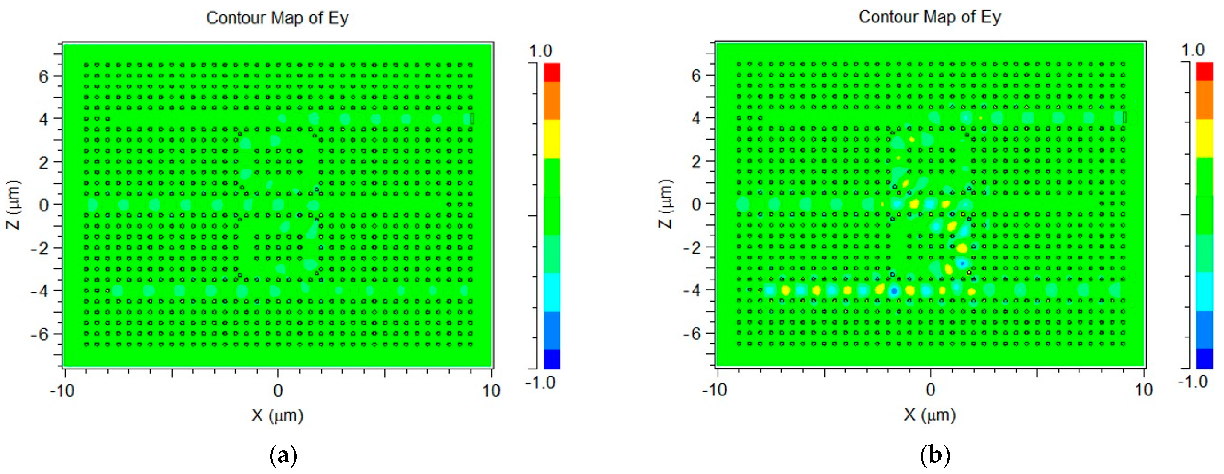
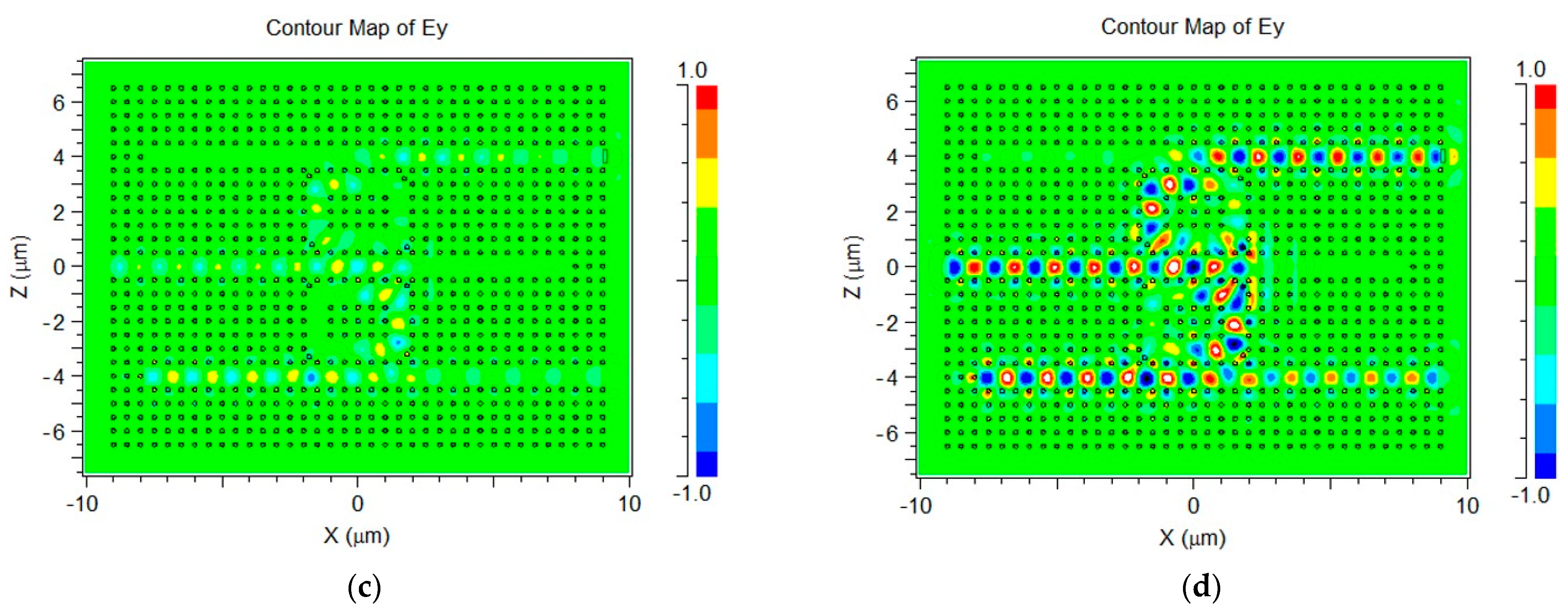
Figure 5a,d show the light propagation of the two input Gaussian pulses through the PC configuration of the optical AND gate for different logic states.
Figure 5a,d show the transmission of the Gaussian signals through the PC configuration of the AND gate. The signals propagate through the two horizontal corresponding waveguides; the lower input signal couples to the corresponding RR and combines with the upper input signal. The combined signal couples to the other RR and continues to the output signal.
Figure 5a represents the case where the input powers of the Gaussian signals A and B are 0.1 W. The signals decay through the RR, and a low-intensity signal travels through the output waveguide, the value of which was determined by the simulation result to be 0.12 W.
Figure 5b represents the case where the input power of the Gaussian signal A is 0.1 W, and the input power of the Gaussian signal B is 0.9 W. The signals decay through the RR, and a low-intensity signal travels through the output waveguide, the value of which, determined by the simulation result, is 0.17 W.
Figure 5c represents the case where the input power of the Gaussian signal A is 0.9 W, and the input power of the Gaussian signal B is 0.1 W. The signals decay through the RR, and a low-intensity signal travels through the output waveguide, the value of which, determined by the simulation result, is 0.27 W.
Figure 5d represents the case where the input powers of the Gaussian signals A and B are 0.9 W. The signals amplify through the RR, and a high-intensity signal travels through the output waveguide, the value of which was determined by the simulation result to be 0.85 W.
Table 1 summarized the inputs and outputs results for the AND gate for all logic states.
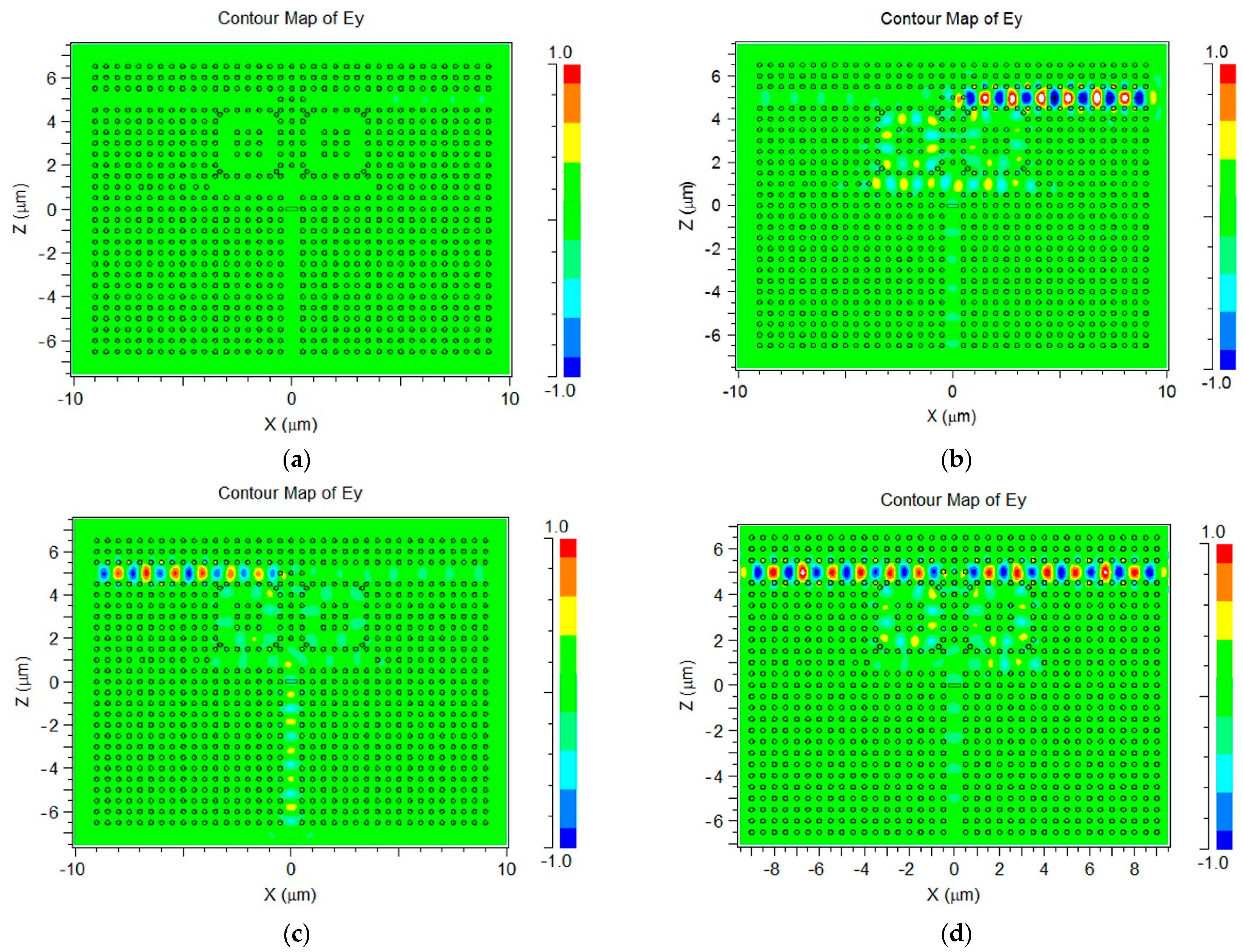
Figure 6a–d show the working state of the logic gate XOR for different states of inputs A and B.
Figure 6a–d show the transmission of the Gaussian signals through the PC configuration of the XOR gate. The signals propagate through the two upper horizontal corresponding waveguides; then, their energy is transferred by light coupling to the corresponding RR, which leads them to the T-combiner region, which combines the two signals into the output waveguide Lvc.
Figure 6a represents the case where the input powers of the Gaussian signals A and B are 0.1 W. The signals decay through the RR, and a low-intensity signal travels through the output waveguide, the value of which, determined by the simulation result, is 0.2 W.
Figure 6b represents the case where the input power of the Gaussian signal A is 0.1 W, and the input power of the Gaussian signal B is 0.9 W. The signals amplify through the RR, and a high-intensity signal travels through the output waveguide, the value of which, determined by the simulation result, is 0.9 W.
Figure 6c represents the case where the input power of the Gaussian signal A is 0.9 W, and the input power of the Gaussian signal B is 0.1 W. The signals amplify through the RR, and a high-intensity signal travels through the output waveguide, the value of which, determined by the simulation result, is 0.81 W.
Figure 6d represents the case where the input powers of the Gaussian signals A and B are 0.9 W. The signals decay through the RR, and a low-intensity signal travels through the output waveguide, the value of which, determined by the simulation result, is 0.26 W.
Table 2 summarized the inputs and outputs results for the XOR gate for all logic states.
The stabilization time can be described as the time it takes for the signal at the output port of a logic gate to reach a stabilized state of intensity, such that a logic state can be determined.
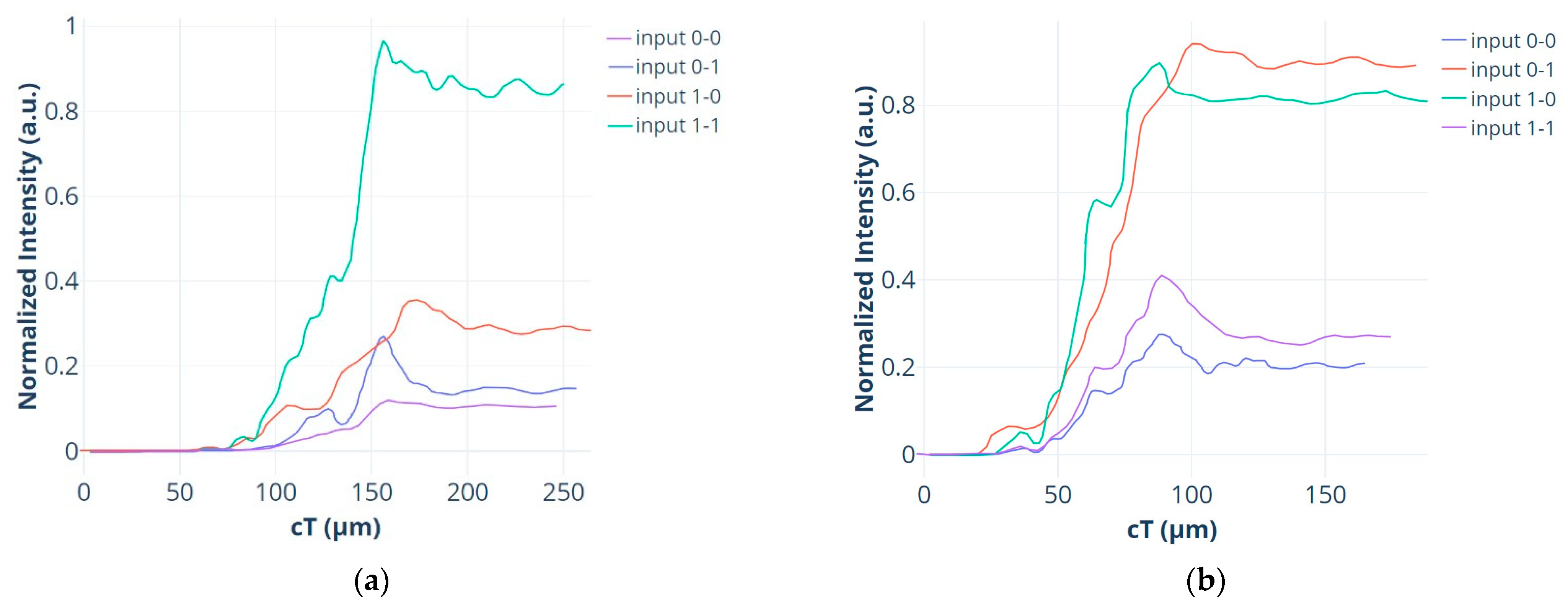
Figure 7a represents the light intensity at the output as a function of time multiplied by the speed of light for the AND gate for the different states of inputs A and B.
Figure 7b represents the light intensity at the output as a function of time multiplied by the speed of light for the XOR gate for the different states of inputs A and B. The stabilization time for each logic gate can be determined from the previously mentioned figures. The stabilization time for the AND gate is 0.66 psec, and for the XOR gate, it is 0.4 psec.
The stabilization intensity is the normalized intensity of the signal at the output of the logic gate when the stabilization time is reached.
Figure 7a shows the stabilization intensity for the AND gate for the different states of inputs A and B. When the input is A = 0 and B = 0, the normalized intensity is greater than 11% and reaches 13%, and the stabilization intensity is 12%. When the input is A = 0 and B = 1, the normalized intensity is greater than 16% and reaches 27%, and the stabilization intensity is 17%. When the input is A = 1 and B = 0, the normalized intensity is greater than 26% and reaches 37%, and the stabilization intensity is 27%. When the input is A = 1 and B = 1, the normalized intensity is greater than 83% and reaches 98%, and the stabilization intensity is 85%.
Figure 7b shows the stabilization intensity for the XOR gate for the different states of inputs A and B. When the input is A = 0 and B = 0, the normalized intensity is greater than 19% and reaches 27%, and the stabilization intensity is 20%. When the input is A = 0 and B = 1, the normalized intensity is greater than 85% and reaches 93%, and the stabilization intensity is 90%. When the input is A = 1 and B = 0, the normalized intensity is greater than 80% and reaches 91%, and the stabilization intensity is 81%. When the input is A = 1 and B = 1, the normalized intensity is greater than 24% and reaches 40%, and the stabilization intensity is 26%.
It can be observed from
Figure 7a,b that the maximum normalized intensity is higher than the stabilization intensity level. This phenomenon can be explained by the power loss in the light-coupling mechanism from the RR and the light reflection coming from the Si rods in the PC structure. In other words, the time the light travels inside the RR and the light reflection coming from the Si rods cause a time delay until the point when the light intensity is stable from these effects, as can be seen in
Figure 7a,b.
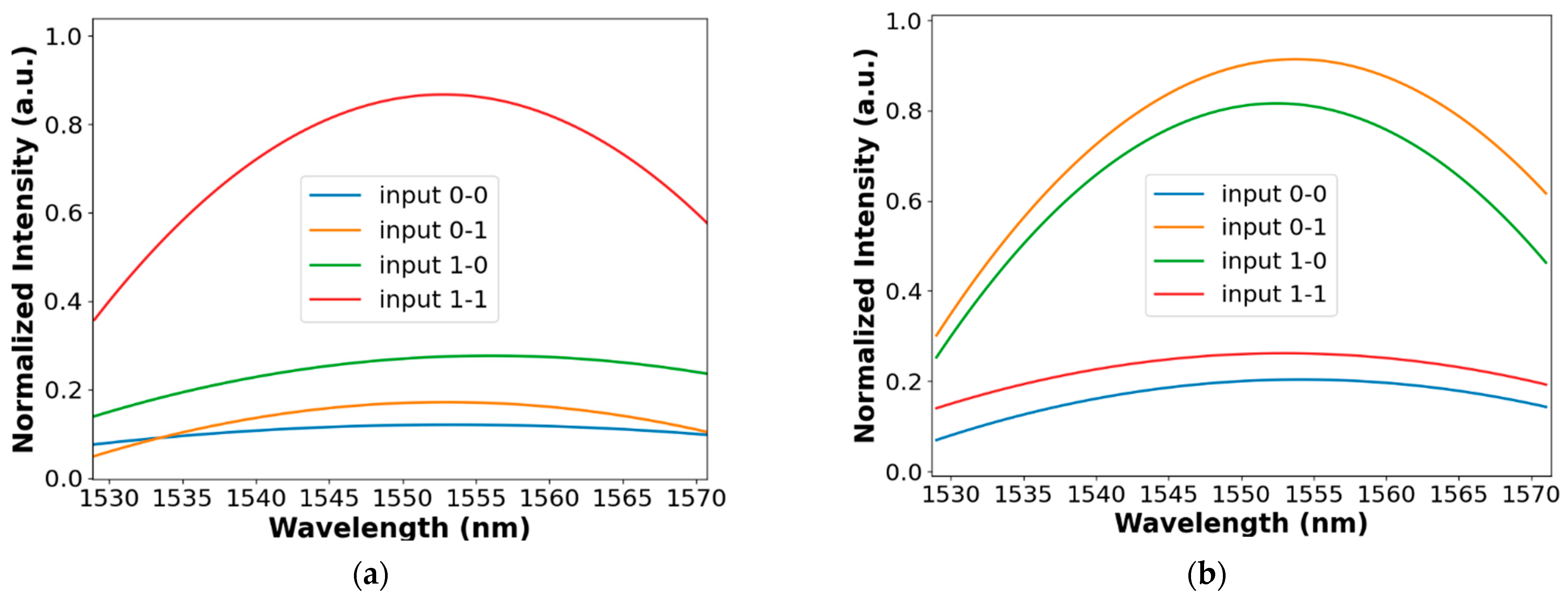
Figure 8a,b show the optical spectrum of the logic gates AND and XOR over the C-band range. It can be noticed that our proposed design can function well with a minor shift of ±5 nm from the operating wavelength of 1550 nm. Thus, our proposed HA can handle the laser drift effect of the source that can happen because of the laser heating process.
The maximum and minimum contrast ratios can be calculated using Equation (6). The ratios extracted for the AND gate from
Figure 7a and
Figure 8a are 8.55 dB and 5.03 dB, respectively. The maximum and minimum contrast ratios extracted for the XOR gate from
Figure 7b and
Figure 8b are 6.53 dB and 4.93 dB, respectively.
The insertion losses of the AND and XOR gates can be calculated by obtaining the normalized intensity as a function of the wavelength from
Figure 8a,b and using Equation (7).
Table 3 contains the insertion loss values over the C-band spectrum for each input logic state for both AND gate and XOR gate.
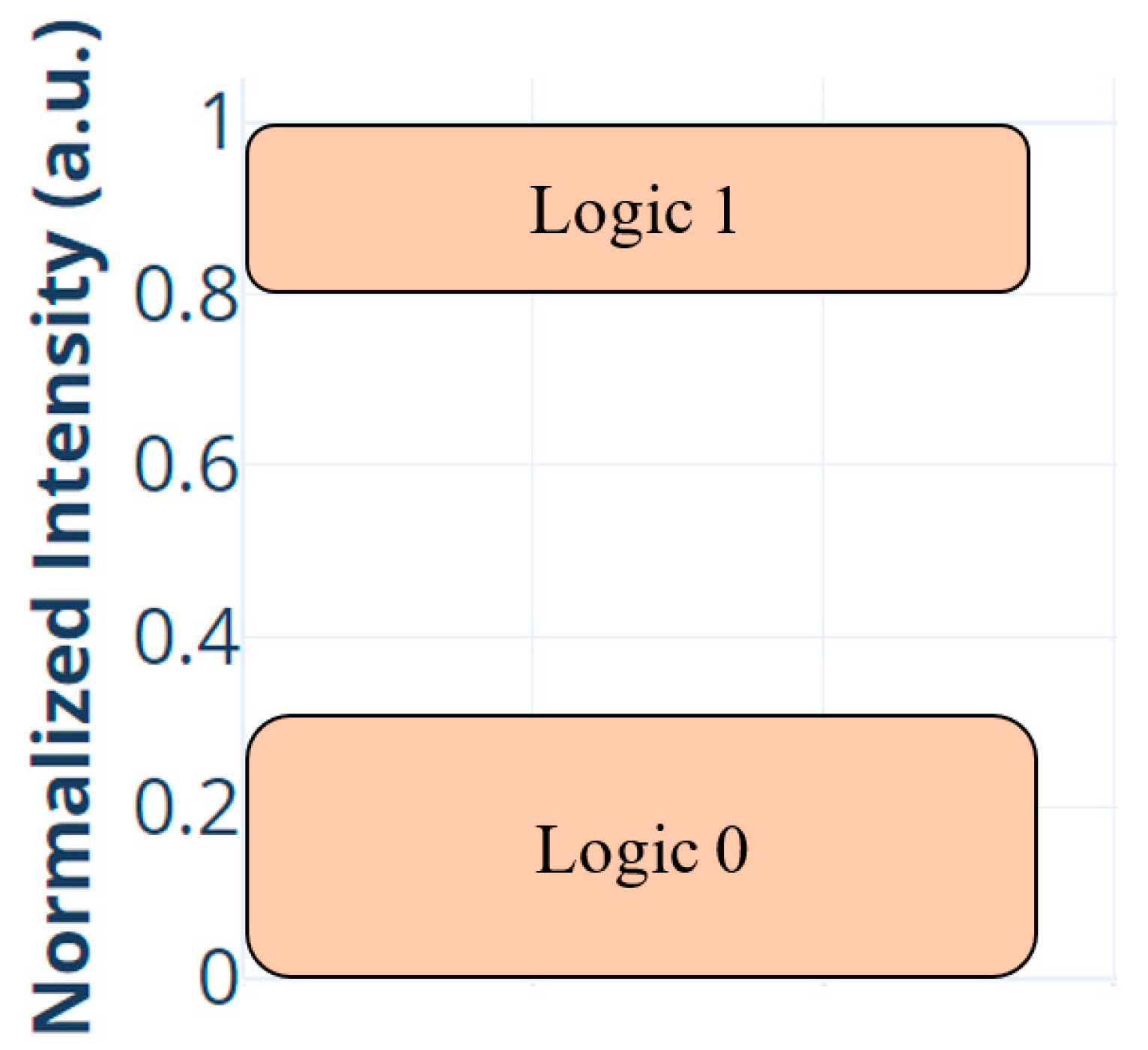
Figure 9 is based on the results of the light intensity at the output of the XOR gate and AND gate for the different states of inputs A and B, shown in
Figure 7a,b and
Figure 8a,b. The logic ranges were determined by the point on the graph where the normalized intensity fluctuates around the same point and settles into a stabilized state.
Logic 0 is defined between 0 to 0.27 normalized intensity, and logic 1 is defined between 0.81 to 1 normalized intensity. Thus, the device has a narrow power range that can be utilized to better define the separation between 0 and 1 logic states.
In
Table 4, a comparison is shown between the HA design introduced above and other HA structures previously proposed in published papers. As shown in
Table 4, the main characteristics of the HA that were compared are stabilization time, logic state 0 range, logic state 1 range, and dimensions. All compared HA devices function at the C-band spectrum.
From
Table 4, it can be concluded that the main benefit of the proposed design is the small logic state range in comparison to other HA devices. This means that our device has the best stability to deal with logic errors that can happen in the detection system.
