Abstract
Charge and spin density waves are typical symmetry broken states of quasi one-dimensional electronic systems. They demonstrate such common features of all incommensurate electronic crystals as a spectacular non-linear conduction by means of the collective sliding and susceptibility to the electric field. These phenomena ultimately require for emergence of static and transient topological defects: there are dislocations as space vortices and space-time vortices known as phase slip centers, i.e., a kind of instantons. Dislocations are statically built-in under a transverse electric field; their sweeping provides a conversion among the normal carriers and condensate which ensures the onset of the collective sliding. A special realization in a high magnetic field, when the density wave is driven by the Hall voltage, originated by quantized normal carriers, reveals the dynamic vorticity serving to annihilate compensating normal and collective currents. Spin density waves, with their rich multiplicative order parameter, bring to life complex objects with half-integer topologically bound vorticities in charge and spin degrees of freedom. We present the basic concepts and modelling results of the stationary states and their transient dynamics involving vorticity. The models take into account multiple fields in their mutual non-linear interactions: the complex order parameter, the self-consistent electric field, and the reaction of normal carriers. We explore the traditional time-dependent Ginzburg–Landau approach and introduce its generalization allowing the treatment of intrinsic normal carriers. The main insights and illustrations come from numerical solutions to partial differential equations for the dissipative dynamics of one and two space dimensions.
1. Introduction
Embedded or transient topologically non-trivial configurations [1,2] are common among symmetry broken ground states [3]. Numerous applications involve particle physics [4], cosmology [5,6], quantum liquids [7,8,9], gases [10], optical condensates [11], cold atoms [12], and liquid crystals [13,14].
More specifically, solid states bring to life domain walls and discommensurations in superstructures [15], current vortices in superconductors [16], displacements vortices as dislocations [17], phase slips and vortices in sliding superstructures (discussed in this article), and walls and skyrmions in magnetic media [18,19,20]. The ground states with spontaneously broken symmetries are ubiquitous in correlated electronic systems. Among them is the vast family of electronic crystals (see review [21] or collection [22]) which includes charge and spin density waves (CDW, SDW), Wigner crystals, stripe arrays, charge ordering states, electronic ferro- and antiferroelectrics, and superstructures in spin singlet systems under a magnetic field: spin-Peierls state, spin-polarized density waves (DW) and superconductors. The ground state degeneracy tolerates the formation of various topologically protected configurations connecting equivalent, but different, ground states. These topological defects include macroscopic extended objects (plane domain walls, dislocation lines, phase vortices), and microscopic ones (various solitons and instantons.)
The electronic crystals can be incommensurate with the underlying host lattice; consequently, their number of unit cells is not fixed. This allows them to absorb excess electrons into the extended (with a different number of total DW periods) ground state. These super-lattices, particularly incommensurate CDWs, SDWs [21,23,24,25] and Wigner crystals [21], are able to perform the collective current conduction (Frölich conductivity [21,23,26]) by means of sliding. Here, the topological defects are crucial for the conversion between normal and collective currents and they also appear in de-pinning processes to initiate sliding in the presence of host defects and constraints. The exchange among normal and condensed charge carriers comes from their imbalance or a stress from the electric field. The steps involve topologically non-trivial objects, such as amplitude and phase solitons, and phase vortex dislocations, which proceed via transient phase slip processes, i.e., the space-time vortices [27,28]. This results in a rich complex of non-linear and non stationary behaviours with vast experimental observations.
In this article, we mostly address DWs which are ubiquitous in quasi one-dimensional (1D) systems [23,24]. We concentrate on a phenomenological description, which is already quite complicated involving coupled equations for order parameters, the self-consistent electric potential, and the density and current of normal carriers interacting with both fields. The main tool used are numerical solutions to these equations, yielding configurations involving static and dynamic topological defects.
The structure of the article is as follows. In Section 2, we outline the basic properties and regimes of DW sliding and deformation. In Section 2.1, we describe the approach based on intuitive phenomenological equations for the CDW order parameter interacting with the self-consistent electric field and extrinsic normal carriers. In the Section 3 we introduce the generalized GL phenomenology. It takes into account explicitly the effects of intrinsic normal carriers and avoids problems with the conservation of condensed density, inherent to the traditional approach of the Section 2.1. Section 4 addresses the special circumstance of CDW sliding driven by the Hall voltage under a high magnetic field. Section 5 discusses more complicated configurations allowed for the rich order parameters of the SDW. We address the scenario of splitting conventional dislocations into combined objects of topologically bound half-integer vortices of the phase and magnetic components. Finally, Section 6 summarises our conclusions.
2. Basic Properties and Regimes in Sliding Density Waves
CDWs [23,24] and SDWs [25] are directly observed as sinusoidal periodic modulations which perturb the electronic density together with atomic distortions for CDWs or electronic spin polarization for SDWs. The DW deformations are characterized by the superstructure wave vector , the normalized amplitude , and the phase . These macroscopic quantum states [26] can be described by a complex scalar-order parameter for the CDW and a complex vector for the SDW:
Phenomenologically, a quasi 1D DW can be viewed as an elastic uniaxial crystal with distortions of the phase playing the role of conventional displacements. The relationships between DWs and the traditional notion of conventional crystals, their elasticity and topological defects, such as dislocations [29,30], are summarized in Table 1.

Table 1.
Relationships between DWs and conventional crystals.
Here a is the host crystal period, is the DW equilibrium wave number, and is the unit vector of the staggered magnetization in a SDW, where (with x being the coordinate in the chains’ direction and location ).
As DWs are electronic crystals, their deformations are charged giving rise to long-range Coulomb forces which result in anomalous elasticity. Properties of all macro- and microscopic topological defects, their interactions, and transformations, are strongly affected by the Coulomb energy [31,32].
Commonly, the sliding DW current is driven by the electric field along the chains; therefore, the collective and normal currents flow in the same direction x. The current conversion near contacts progressively gives rise to the collective current, resulting in a stationary equilibrium in the bulk. The conversion of the injected current of normal electrons (or holes) into the collective DW current and back requires adding electronic crystal planes near the contact source and their elimination near the drain. In thick channels that proceeds via a transverse flow of dislocations [33,34] which can be viewed as the leading edges of the penetrating/retreating planes, while in wires the plane phase slips are expected to be formed (see [28] for a review). In any case, an extended distribution of these topological events is formed, as identified in CDWs by space-resolved X-ray diffraction [35,36].
Dislocations, as electronic vortices, can be initiated statically when the lateral electric field is applied transversely to the chains’ orientation [37], or due to variations in near the surface [38], or because of thermal hysteresis of [39]. All of this provides a rich complex of non-linear and non stationary effects, partly illustrated in Section 2.1 and Section 3.
In superfluids or superconductors, vortices can move in any direction transverse to their axis. However, for dislocations there are two types of motion [17]: conservative (glide) and non-conservative (climb). A glide along the Burgers vector passes freely, while a transverse to the Burgers vector climb requires an inflow of addatoms or vacancies (electrons and holes, or their polaronic states [15] for electronic crystals). Specifically for DWs, when a dislocation climbs across a chain, the phase increment along the chain changes by , i.e., one period is added/removed; thus, two electrons are absorbed/emitted from/to the reservoir of normal carriers. Thus, the climb of dislocations, the rarest process in conventional crystals, becomes obligatory in sliding electronic crystals, while the common glide is less important. Considering these events on average, we arrive at a new multi-fluid hydrodynamic system involving conventional and topological objects [40].
A peculiar realization [41] of CDW sliding can be achieved using mesa-junctions under an external high magnetic field, where sliding can be driven by the Hall voltage originating from the transverse current of normal carriers. Here, unusually, the collective and normal currents move in opposite directions, allowed to be exactly compensated for so that the total current is zero. The zero-sum loop of the collective current is compensated exactly by the counter current of normal electrons. This promotes their annihilation at the boundaries of the open circuit design, which is provided by periodic phase slip processes seen as spontaneous coherent oscillations.
The rich order parameter of the SDW allows for complex topological defects where phase displacements interfere with the magnetic orientation [42]. Thus, the half-integer -vortices or phase slips can appear in SDWs, while they are forbidden in CDWs where only self-mapping phase circulations are allowed. With assistance from Coulomb repulsion forces, the conventional dislocations lose their priority bringing to life an unusual topological object, constructed by the combination of a half-integer dislocation and a semi-vortex of the staggered magnetization.
DW deformations and movements are realized through interacting and exchanging with a sea of normal carriers present as extrinsic and intrinsic carriers. The extrinsic carriers come from pockets on the Fermi surface which are not connected by the CDW wave number or even belong to another electronic band; therefore, they do not participate in DW formation. They only interact with the charged DW deformations via the common electric potential . The intrinsic carriers belong to bands participating in DW formation; they can be activated across the DW gap or injected, thus mutually influencing the DW amplitude. Importantly in our context, they are also affected by DW phase deformations, so that the total potential energy V for intrinsic carriers can be written as:
where and are the Fermi velocity and the related DOS in the parent metal, respectively, and is the Fermi energy shift coming from the DW briefing .
With this in mind, our numerical simulations are presented in two approaches:
- (i)
- the minimal Ginzburg-Landay type model, where all intrinsic carriers are prematurely integrated out [43,44];
- (ii)
- a deeper and more complicated model [45] exposing the intrinsic carriers explicitly.
In both cases, we take into account multiple fields in their mutual non-linear interactions: the amplitude A and the phase of the order parameter, distributions of the electric potential , of the density n, and the current j of normal carriers. The results of the numerical modelling for the static, stationary, and transitory effects in CDWs are presented in Section 2.1 and Section 3.
The approaches tested for CDWs are extended in Section 5 to a more complicated SDW case. For both CDW and SDW, a spontaneous origin of dislocations and vortices is achieved without seeding or promoting their formation.
2.1. The Ginzburg–Landau Type Model for the CDW
In this section, we study the CDW dynamics within the dissipative time dependent Ginzburg–Landay (TDGL) type model. Generically this approach can be traced back to the phenomenological equation for relaxation of the order parameter determining the energy functional . It has been widely used (analytically, e.g., [46] and numerically, e.g., [10,47]) for non-equilibrium pattern formations, particularly with the appearance of topological defects when quenching across a phase transition. The parameter can be complex, interpolating with the Gross–Pitaevskii equation for a Bose condensate, allowing the inclusion of the quantum coherent states of polaritons or cold atoms. In this approach for fermionic systems, originally developed for superconductivity (see [16,27]) and extended to CDWs (see [48,49]), the intrinsic carriers are integrated out giving rise to coefficients of amplitude expansion and gradients of the order parameter; while extrinsic carriers from the bands not involved in CDW formation are taken into account explicitly (if present).
The density (per unit length of one chain) of the energy functional can be written as:
Here the overall coefficient comes from the microscopically derivable terms and , parameters describe CDW interchain coupling, is the free energy of extrinsic carriers, and is the host dielectric constant. The coupling of the phase with the electric potential comes from the fact that within the Ginzburg–Landau scheme is the charge density distribution originated from phase deformations. The amplitude A is normalized such that the energy of a homogeneous state has a minimum at . Various forms for , such as generic expansion or the broader energy dependence of the Peierls–Froehlich microscopic theory, can be input akin to the BCS:
where and are the microscopic parameters: the electronic gap and correlation length, and are numerical coefficients (functions of T).
The time evolution, assuming a dissipative regime, is described by functional derivatives of W in Equation (3) with respect to and :
here and below, for brevity we only show derivatives over one transverse coordinate y.
The concentration of normal carriers obeys the diffusion equation
Notice that, contrary to common minimal Ginzburg–Landau models [16,27,49] that only contain equations such as (5) and (6) for the order parameter, we include two more: the Poisson Equation (7), coupling collective and normal extrinsic charges through the potential ; and the diffusion equation for the carriers (8). Boundary conditions for these partial differential equations (see [43,44]) take into account that the normal CDW stress and normal electric field (confined within samples) vanish at all boundaries, and the normal current flow only exists at source–drain boundaries.
Below we discuss the results of the numerical solutions to the above equations in a rectangular geometry for two cases corresponding to different applications of the electric voltage: longitudinal and transverse.
For a transversely applied electric field, our simulations (see [43,44] for more examples) recover a fast initial creation of multiple dynamical vortices evolving to their smaller equilibrium number. The snapshots of a multi-vortex transient process in Figure 1 (left panel) illustrate vortices nucleations at opposite boundaries and their traversing of the sample with their mutual annihilation or absorption at another boundary (plot a). Only a small number of static vortices are left at the final stage (plot b). An isolated vortex is shown in detail in the right panel.
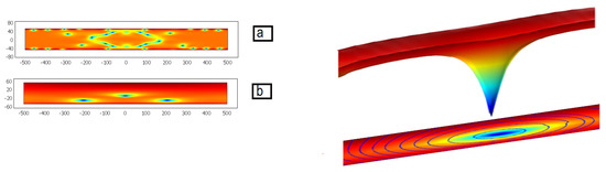
Figure 1.
Left panel: 2D presentation of the CDW amplitude A. Upper plot (a): a snapshot of the transient state with many intermittent vortices. Lower plot (b): the final state with only three remaining vortices showing a tendency to form a triangular lattice. Right panel: 3D plot of the amplitude of a single CDW vortex in the final state. On the basis: the density plot of A with stream lines of the phase.
For a longitudinally applied voltage, the main interest lies in observing the space-time vorticity giving rise to phase slip processes. This one-dimensional regime has already been addressed in numerical simulations [50,51,52] based on minimalistic equations derived microscopically [28,49] for a dirty limit near the transition temperature. Contrarily, our multiple equations were designed for a pure system with a well-established gap in the fermionic spectrum where the self-consistent electric field and the reaction of normal carriers become important. For shortness, in Section 4 we demonstrate results for a special case of sliding under an HMF.
2.2. Coulomb Hardening, Anomalous Energy and Shape of Charged Dislocations in DWs
The strong contribution of Coulomb interactions to the energetics of dislocations is very important for their properties which may have a qualitative effect as will be discussed in Section 5. Here, we shall provide some necessary estimations which can be tuned by analytical solutions to some cases [31,37].
In a static linear regime with a constant amplitude (i.e., sufficiently far away from the amplitude node), the Coulomb potential and the normal carriers can be excluded from the GL free energy (3). In the Fourier phase representation , the resulting energy can be written as
with
where is the compression modulus, is the share modulus which comes from the interchain coupling yielding the 3D transition temperature . The last term is due to Coulomb interactions of charged phase deformations, taking into account the screening by normal carriers.
Let the phase be deformed in a volume with characteristic lengths and determined, for example, by a dislocation loop or a dipole of dislocation lines. At distances below the screening length the energy (9) can be estimated as
At the monitored , the dependence of on is non-monotonous. Minimization over results in the optimal length and energy
where and are the number of chains embraced by the dislocation loop. We can see that for non-screened Coulomb interactions the dislocation energy obeys the area law (), growing much faster than according to the usual perimetric law () law.
At large distances , the analytical (in ) form of the elastic energy is restored, while with an enhanced compression module:
At low T the normal carriers are frozen out, , causing the divergence of the comprehensibility (“Coulomb hardening” effect [53]) under the simultaneous action of Coulomb interactions and screening carriers. For a dislocation, the standard perimetric law is restored with the dislocation energy enhanced as . Nevertheless, the creation of dislocations, in spite of their big energy at a small , is allowed requiring higher applied potentials.
For another important geometry, consider a straight dislocation line positioned at a depth Y below the lateral junction surface. For screened Coulomb interactions at , the dislocation energy (per unit of its length) obeys the traditional vortex lines logarithmic law, but quantitatively it is greatly enhanced as . At low T there is an intermediate wide region where a confinement law is set up with . A constant force with a linear density acts upon the dislocation line requiring the application of an electric field with a definite threshold.
3. Generalized Ginzburg–Landau Type Model for CDW Vortex Formation
Within the traditional GL approach presented in the previous section, the intrinsic electrons are excluded (“fermions are integrated out”) at the microscopic level. All observable quantities characterizing the CDW are determined via the order parameter alone. Now we consider the generalized GL-type theory [42,45] which explicitly accounts for intrinsic carriers and their interaction with the order parameter. The theory can be further extended [40] to include the possible extraction/reabsorption of normal carriers from/to the CDW collective density which proceeds via the formation of topological defects. This approach provides deeper insights into the partitions of the normal and collective charges and currents at the expense of specific numerical modelling difficulties as the theory is now non-analytic with respect to the order parameter.
The on-chain energy density can be written as [42,45]:
Here, for brevity we do not show terms related to transverse gradients or extrinsic carriers which are the same as in (3); also we omit the index “” as . The order parameter amplitude A is connected with n via the energy which must have a property that its minimum over A disappears when n surpasses a critical value above which the CDW state is erased. Unlike the generic GL case, the terms containing and ( are not multiplied by making them singular near the vortex core when . Originating from the chiral anomaly [42,45], they cannot be derived perturbatively. However, altogether the contribution of non-analytic terms vanishes when . This hidden compensation can be proven by excluding n from the equations of motion which, in general, cannot be performed explicitly, rather than with the help of additional approximations [45].
The time evolution equations acquire the form (we only show only one transverse coordinate y):
Contrary to the former GL equations described in the previous section, now Equations (11)–(13) are non-analytic concerning the order parameter [45].
As before, we consider the kinetics of the carriers in the quasi-equilibrium diffusive approximation with the important peculiarity that they experience combining the potential V from (2), rather than just :
Here , and are the conductivities, the chemical potential, and the electrochemical potentials of intrinsic carriers, respectively. We define the normal and collective charge densities as
In the metallic phase and ; with the development of the CDW gap, grows reaching the equilibrium at when .
To proceed with the numerical solutions to the above equations, we must add, as before, the boundary and initial conditions. The initial conditions are commonly chosen as
Boundary conditions for A can be chosen as either or with being a normal to the boundary. For the function we use the simplest expression:
where the coefficients . Here, the first term comes from the normal metal, and the two other terms present the Landau-type expansion in A at the proximity of the nominal transition temperature . The actual transition is shifted locally by the presence of normal carriers with a critical concentration of where is the correlation length. Thus, we obtain
Our numerical results presented below demonstrate the possibility of vortex creation when the applied electric field or monitored current are above their thresholds. Figure 2 illustrates a one-dimensional regime corresponding to experimentally typical whisker crystals. We observe the nodes of the DW amplitude located at both sides of the sample; they correspond periodical in time in the phase slip processes. Figure 3 illustrates a two-dimensional regime in a film with an electric field applied transversely to the CDW displacements. The achieved appearance of the static array of dislocations might be relevant to the experimentally observed step-wise reconstruction of mesa-junctions [54].
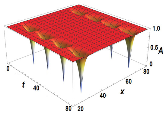
Figure 2.
A sequences of phase slip events near the two sample boundaries. They are seen as sets of nodes of the DW amplitude .
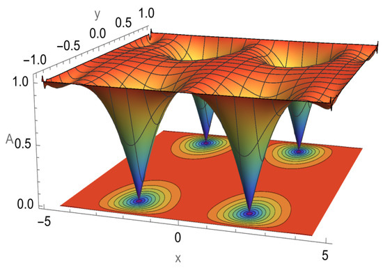
Figure 3.
A fragment of a static array of dislocations appearing near sample boundaries under an electric field applied transversely to direction x of DW displacements.
4. CDW Sliding and Vorticity under a High Magnetic Field
Commonly, the sliding CDW current is driven by the electric field (in direction x of the chains), which penetration is mediated by the normal current density in the same direction. The sliding and normal currents flow in the same direction x experiencing a gradual conversion towards the equilibrium. The normal current dominates at a junction; it gradually fades giving rise to the collective current until the equilibrium is reached for the bulk stationary regime [35,36].
New astonishing circumstances have appeared with experiments on mesa-junctions under a high magnetic field (HMF) [41,55]. It was found that the CDW can be driven by the Hall voltage along the chains’ direction x, generated by a normal current running in a transverse interchain direction y. Moreover, the collective and normal longitudinal currents now move in opposite directions; furthermore, they are completely compensated so that the total current is zero. The zero-sum loop of the collective current, exactly compensated for by the counter current of normal electrons, promotes their annihilation at the boundaries of the open circuit design, enacted by periodic phase slip processes seen as spontaneous coherent oscillations.
Following the experimental geometry, the Hall bar was formed across the CDW chains; the magnetic field and bias normal current were applied orthogonally in the interchain directions z and y correspondingly, producing the Hall voltage in the direction of the chains with a short length . According to experiments, the magnetic field must be sufficiently high such that the carriers are quantized and only occupy the lowest Landau levels (LL). This level can acquire as much as electrons per unit area where is the magnetic length, so the LL filling per chain is , where is the mean concentration of normal carriers with a local value of . In this regime of the extreme Landau quantization, the density is determined locally by the electric potential . The profile for the density of carriers per chain is where is the Fermi distribution function.
There are basic local relations
Here, the relations (18) are common to the conventional GL picture in Section 2.1; they provide the commonly used definitions of the collective density and current; and are coupled by Equation (19) in the local electroneutrality approximation which is the limit of the Poisson Equation (7).
The entangled evolution of and are described by the basic time-dependent GL equations:
where Equation (21) is the resolution for as a function of of Equation (19), and is the pinning force which disappears after the onset of sliding. These equations were solved for a sample with a width of l with boundary conditions ; boundary values of the potential were turned on, in view of the unique relation (21), via and , following smooth switching .
The regime of depinned sliding with is illustrated in Figure 4. This shows a generated sequence of periodic phase slips where the CDW phase acquires steps Figure 4, Left panel). With phase slips as the space-time vortices (Figure 4, Right panel), the amplitude passes through zero at their cores. With our parameters, it is not completely restored between the nodes, so a persistent dip is formed from which periodically shoots to zero (Figure 4, Center panel). This figure explains the generation of the experimentally observed coherent oscillations [41] which frequency is proportional to the bias voltage along the Hall bar.
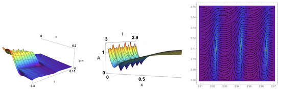
Figure 4.
Plots of the spatio-temporal evolution from modelling the periodic phase slips: Left panel: the 3D plot of the phase ); Center panel: the CDW amplitude ; Right panel: streamlines on the amplitude density plot for the vector . A sequence of three phase slip events is observed with the amplitude nodes located near .
Consider the depinning regime of CDW sliding when the driving force (the Hall voltage) just exceeds the threshold [41]. We use the same set of equations with a necessary simplification to fix the CDW amplitude in the bulk. We model the pinning force in such a way that it starts with the linear law and then sharply drops towards zero at , where is the threshold phase displacement of depinning:
Here is the pinning length which value can be taken from the experiments, and is a modelling parameter. The space-temporal evolution of the amplitude and the phase are presented in Figure 5. The modelling reveals the formation of depinning propagating fronts created at the sample boundaries. The fronts collide, first forming a short peak of the phase velocity ; subsequently, the fronts annihilate giving rise to the sliding regime at still inhomogeneous distributions of the electric field and particle density.
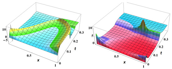
Figure 5.
Evolution of the depinning process: Left panel: the self-consistent driving electric field with given by Equation (21); Right panel: the phase velocity .
We summarize the content of this Section as follows. Application of a high magnetic field, normal carriers in residual pockets left after CDW formation can be brought to a quantum state at low Landau levels. When forced to carry a transverse current, the carriers generate a Hall electric field in the chains’ direction which brings the CDW background to the collective sliding. Ensuring the Hall geometry has no source/drain junctions in the sliding direction, the collective current enforces the on-chain component of the normal current, exactly compensating for the two counter currents. The annihilation of the counter currents takes place near the boundaries via the space-time vortices of the CDW phase around the enforced amplitude nodes resulting in a regular sequence of the phase slips. For the first time, to our knowledge, the simplicity of Equations (due to the local relation (21) of the electric potential and the carriers’ concentration) allows to model the depinning process when the depinning fronts are nucleated at the edges and develop into the bulk with their subsequent annihilation.
5. Combined Topological Defects in Spin-Density Waves
Systems with spontaneous symmetry breaking with respect to a complex multi-component order parameter may offer an intriguing possibility for non-integer vorticities in subspaces of their degeneracy (see [56]). Fractional vortices have been investigated in the superfluid helium A ([57,58], triplet superconductors [59,60], FFLO phase [61,62] and Bose-condensate of polaritons [63]. Following the suggestion of a fractionalization of the spin vortex in an anti-ferromagnetic crystal in presence of a frozen-in dislocation [64], the regular presence of combined topological defects have been suggested [65] for a sliding SDW state which is explored below.
5.1. Half-Integer Complexes of Vortices and Dislocations in SDWs
Contrary to conventional vortices created in CDWs [65], in SDWs the complex topological objects can appear as half-integer -phase vortices combined with half-integer spin rotation. The SDW order parameter (1) allows for three options of its self-mapping which are determined by partial vorticities and in the SDW phase and its magnetization direction.
- (i)
- The phase dislocation , i.e., the pure phase vortex , while stays intact: and , where and ;
- (ii)
- The - vortex where performs the full rotation while the phase stays intact: and , where and ;
- (iii)
- The combined object : and , where and . In this case, the two factors of the SDW order parameter change the sign together, but their product leaves constant.
The distribution of near the combined half-integer vortex is illustrated schematically in Figure 6.
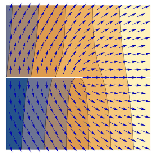
Figure 6.
Configurations of the half-integer combined vortex in the SDW: vector plot of the magnetization on top of the contours of the positional phase . The white line drawn to the left from the defect centre carries no physical singularity: the visible discontinuity in the direction of is compensated by the jump in .
The energy density in the SDW encompasses two parts: . The charged part originating from the phase displacements is common to both CDW and SDW; it is given by Equation (10). The magnetic part has the form
where the moduli characterizes the rotation of the staggered magnetization with the unit vector ; their values are similar to the bare moduli of the phase displacements taken without Coulomb interactions in (10). is the spin anisotropy energy; its effects on the structure of combined topological defects are discussed in the next section.
Since the energies of the vortices depend on their winding numbers as , the common tendency is to reduce to the lowest permissible values. A comparison of energies of the pure phase vortex (phase dislocations ) and combined objects must account for the charge conservation, thus protecting the total phase vorticity . The total magnetic vorticity does not need to be conserved, but should be kept at zero to avoid logarithmic energy divergence at large distances from a non-compensated pair of vortices. The energy divergence of phase dislocations is not a limitation since it is compensated for by the driving electric field. Therefore, it is tempting to consider the spitting of one into two combined objects which follows a decomposition path of a phase vortex into two pairs of half-vortices:
If the energy parameters for phase and magnetic perturbations, and , are comparable as it takes place near to when free carriers screen Coulomb interactions at shortest distances, the consequent dissociation cost is zero: and the result depends on a tiny balance of coefficients. Contrarily, at low T the Coulomb energy of the phase counterpart dominates; therefore, the magnetic vortex energy can be neglected. In this case about a half of the energy is gained by the decomposition of ( which cannot be rejected.
The energy of the pure spin vortex is estimated as at all transverse distances Y among the vortex lines. As demonstrated in Section 2.2, for a pure phase vortex such a form of energy persists for the screened Coulomb interaction at where ; at low T it is greatly enhanced as with respect to . However, except when in close proximity to , the energies of he initial connfiguration and the counterpart of the split configuration are highly enhanced. The energy gain is more drastic at low T at intermediate which is discuss below in Section 5.2 in conjunction with effects of magnetic anisotropy.
Our numerical calculations confirm the spontaneous splitting of the integer phase vortex (Figure 7a) into two half-integer combined vortices (Figure 7a,b).
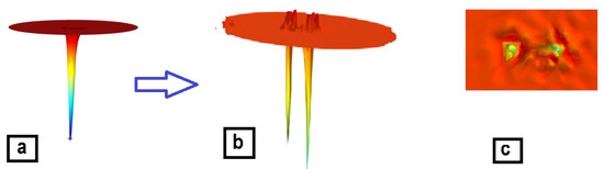
Figure 7.
Calculated profiles of the amplitude for the spontaneous splitting of the bare phase vortex (a) into a pair of combined, phase plus magnetization, half-integer vortices (b and c for the 3D and density plots, respectively).
5.2. Effects of the Spin Anisotropy
There are two cases of the spin anisotropy which still allow for a free rotation of spins, thus validating the above conclusions: (i) a full isotropy or an “easy plane” anisotropy; (ii) an “easy axis” anisotropy under a magnetic field exceeding the spin-flop threshold (the momentum is tilted and a free rotation of the hard plane projection is permitted). However, the known SDW crystals are of low-symmetry, possessing the spin anisotropy in all three directions. Its presence prevents the long-distance rotation of which results in a confinement of the half-integer vortices in pairs connected by a magnetic domain wall. If the anisotropy is weak, it will not affect the arrangement in the vicinity of a vortex, but at large distances the rotation of spins is concentrated within a Neel domain wall. This forms a string (a plane in 3D) which attempts to confine the two combined objects as it is illustrated in Figure 8.
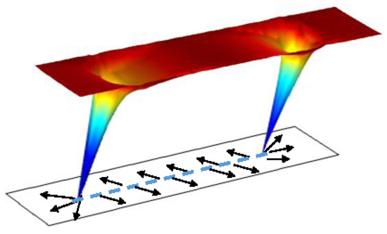
Figure 8.
Two half-integer vortices connected by a Neel domain wall.
The combined objects are composed of the spin and charge semi-vortices. The confinement, due the spin anisotropy, competes with the repulsion, due to Coulomb forces. We now recall (Section 2.2) that the unscreened Coulomb contribution to the vortex energy brings about a linear law instead of the standard logarithmic law. The total energy gain for the pair of combined vortices with respect to the normal phase vortex will be , where and is the number of chains between the combined vortices. The repulsive anti-confinement energy overcomes the energy lost due to domain wall formation , as both possess a similar N dependence. Commonly, is much smaller than , hence the resulting interaction between the two semi-vortices is repulsive. We see that within the screening length both the anisotropy and Coulomb energies grow linearly with distance, with the latter dominating quantitatively. Hence the anisotropy binding energy is overcome by Coulomb repulsion and thus no confinement.
At distances exceeding the screening length , the growth of the Coulomb energy slows down to the conventional, while quantitatively enhanced, logarithmic law (Section 2.2). However, the spin anisotropy energy keeps growing linearly. The total energy gain of the two combined vortices with respect to the dislocation becomes
As this dependence on N is non-monotonous, there exists an equilibrium distance between the two semi-vortices . With the screening being frozen out at low temperatures when , the string length may pass through the whole sample width, typically µm, already at experimentally accessibly low temperatures.
5.3. Combined Topological Defects and Narrow Band Noise Generation
A universal signature of DW sliding is the generation of a coherent periodic unharmonic voltage signal, the so called “narrow band noise” (NBN) (see [23,66]). In CDWs, its frequency is usually proportional to the collective and, remarkably, their ratio universally corresponds to the intuitively clear definitions
The resulting ratio corresponds to the proliferation of two electrons when the CDW is displaced by its wave length . In CDWs the NBN generation was measured directly and the ratio of was definitively confirmed. In SDWs the NBN was observed less precision with a variable ratio (usually small because of the inhomogeneous distribution of currents). Nevertheless, the linear law was confirmed.
Up till now there is no consensus on the origin of the NBN, with two competing views.
(i) The first and largely accepted was the wash-board frequency (WBF) model which suggests extrinsic NBN generation by DW sliding through the periodic host lattice or its defects [23]. Within the WBF model, the NBN frequency in SDWs is doubled with respect to CDWs. This comes from differences in the oscillating densities of the charge or lattice displacements:
because of the disparity of with respect to the time reversal. Within the WBF model, the NBN frequency should be doubled for SDWs with respect to CDWs.
(ii) The phase slip generation (PSG) model assumes that the NBN is generated by phase slip processes created periodically near injection contacts [33,34,48,49,50]. This mechanism looks plausible since the phase slips are already necessary for the current conversion at the contacts, with some concerns on their regularity. Nevertheless, this regularity is clearly reproduced in our modelling, as demonstrated in Section 2.1 and Section 4, in accordance with the experimentally confirmed high coherence of the NBN signal.
(iii) An intermediate scenario can be envisaged for the DW which slides in the bulk, while being pinned at the sample surface. With the coupling energy , the proliferation of at constant would provide the necessary WBF. This separation of moving and pinned layers calls for the successive creation of dislocations, thus constructing a bridge to the PSG scenario. This scenario is also successfully covered within our modelling.
While for CDWs all three scenario give the same ratio , for SDWs an intriguing difference was discussed (see [67,68]): for the PSG mechanisms in (ii) and (iii) and for (i) of the WBF one. Intriguingly, our prediction for chimera defects with combined half-integer vorticities indicates the possibility of , even for the PSG mechanisms (ii) and (iii). Moreover, the ratio can switch between and 1 depending on the temperature. Indeed, the chimeras are energetically favourable at low temperatures in the absence of screening carriers, when the Coulomb energy dominates the phase vorticity. The vorticity of the phase requires a double slip rate to promote the same collective current. However, near the energies of the magnetic and phase vorticities are comparable, so the splitting into half-integer objects is not strongly profitable bringing back from 1 to . As we have explained in the previous sections, the magnetic anisotropy can confine the half-integer object into loose integer pairs, thus re-tuning to for sufficiently narrow samples.
To summarise this section, the sliding SDW generates combined topological objects, where the DW displacement and spin rotations are topologically coupled. These defects lower the Coulomb energy of the conventional phase vortex and are energetically stable. Their formation also leads to a twice reduction in the NBN frequency, which remains an important debatable topic.
6. Conclusions
In the science of electronic crystals, ample research has been devoted to the study of stationary or transient states with static and dynamic topologically non-trivial configurations, such as electronic vortices (dislocations), instantons (phase slip centres), and microscopic soliton complexes. Having been inspired by extensive experiments, we have studied equations for dynamics involving topological objects in density waves under various circumstances. Our models include multiple fields in their mutual non-linear interactions: the phase and amplitude of CDWs, the spin polarization for SDWs, electric field, and distributions of current and density of normal carriers. The numerical solutions to the resulting equations illustrate the emergence of vortices, their turbulent evolution, and the final formation of steady arrays or stationary oscillations.
We have studied several experimentally significant situations, such as proliferations of space vortices under the field effect of a transverse voltage and a coherent sequence of space-time vortices, or phase slips, under longitudinal driving. Furthermore, the sliding driven by the Hall field generated by quantized electrons under a high magnetic field was modelled, revealing an interesting regime of exactly compensated collective and normal countercurrents; their annihilation proceeds via a regular sequence of phase slip processes.
SDWs add an additional richness by combining the common vorticity of the phase with the particular vorticity of modulated magnetization. This gives rise to interesting topological objects with normally prohibited half-integer winding numbers. The standard dislocation splits into two combined topological objects which, in the presence of a weak spin anisotropy, are connected by a string whichconfining tension can be overrun by the Coulomb energy of the phase component. The formation of such combined topological objects results in a two-fold reduction in the NBN frequency, which still remains an essential disputed question.
The combined topological defects link our specific problems with the general issues reported for quantum solids and liquids, particle physics, and cosmology.
Author Contributions
Conceptualization, N.K. and S.B.; methodology, N.K. and S.B.; formal analysis, N.K. and S.B.; writing—original draft preparation, N.K. and S.B.; writing—review and editing, N.K. and S.B. All authors have read and agreed to the published version of the manuscript.
Funding
This research received no external funding.
Data Availability Statement
Not applicable.
Conflicts of Interest
The authors declare no conflict of interest.
References
- Mermin, N.D. The topological theory of defects in ordered media. Rev. Mod. Phys. 1979, 51, 591–648. [Google Scholar] [CrossRef]
- Mineev, V.P. Topologically Stable Defects and Solitons in Ordered Media; Harwood Academic Publisher: New York, NY, USA, 1998. [Google Scholar]
- Bunkov, Y.M.; Godfrin, H. (Eds.) Topological Defects and the Non-Equilibrium Dynamics of Symmetry-Breaking Phase Transitions; NATO ASI Series; Kluwer Academic Publishers: Amsterdam, The Netherlands, 2000. [Google Scholar]
- Skyrme, T.H.R. A non-linear field theory. Proc. R. Soc. Lond. Ser. A 1961, 260, 127–138. [Google Scholar]
- Hindmarsh, M.W.; Kibble, T.B.W. Cosmic strings. Rep. Prog. Phys. 1995, 58, 477–561. [Google Scholar] [CrossRef]
- Vilenkin, A.; Shellard, E.P.S. Cosmic Strings and Other Topological Defects; Cambridge University Press: Cambridge, UK, 2000. [Google Scholar]
- Schiffer, P.; Osheroff, D.D.; Leggett, A.J. Nucleation of the ab transition in superfluid 3He: Experimental and theoretical considerations. Progr. Low Temp. Phys. 1995, 14, 159–211. [Google Scholar]
- Volovik, G.E. The Universe in a Helium Droplet; Clarendon Press: Oxford, UK, 2003. [Google Scholar]
- Eltsov, V.B.; Krusius, M.; Volovik, G.E. Vortex formation and dynamics in superfluid 3He and analogies in quantum field theory. Prog. Low Temp. Phys. 2005, 15, 1–137. [Google Scholar]
- Berloff, N.G.; Svistunov, B.V. Scenario of strongly nonequilibrated Bose-Einstein condensation. Phys. Rev. A 2002, 66, 013603–013610. [Google Scholar] [CrossRef]
- Berloff, N.G.; Keeling, J. Universality in Modelling Non-equilibrium Pattern Formation in Polariton Condensates. In Physics of Quantum Fluids: New Trends and Hot Topics in Atomic and Polariton Condensates; Springer Series 177; Bramati, A., Modugno, M., Eds.; Springer: Berlin/Heidelberg, Germany, 2013; pp. 19–38. [Google Scholar]
- Neely, T.W.; Scherer, D.R.; Bradley, A.S.; Davis, M.J.; Anderson, B.P. Spontaneous vortices in the formation of Bose-Einstein condensates. Nature 2008, 455, 948–951. [Google Scholar]
- Chuang, I.; Durrer, R.; Turok, N.; Yurke, B. Cosmology in the laboratory: Defect dynamics in liquid crystals. Science 1991, 251, 1336–1342. [Google Scholar] [CrossRef]
- Bowick, M.J.; Chander, L.; Sciff, E.A.; Srivastava, A.M. The Cosmological Kibble Mechanism in the Laboratory: String Formation in Liquid Crystals. Science 1994, 263, 943–945. [Google Scholar] [CrossRef]
- Kranjec, A.; Karpov, P.; Vaskivskyi, Y.; Vodeb, J.; Gerasimenko, Y.; Mihailovic, Y. Electronic Dislocation Dynamics in Metastable Wigner Crystal States. Symmetry 2022, 14, 926. [Google Scholar] [CrossRef]
- Kopnin, N. Theory of Nonequilibrium Superconductivity; Oxford University Press: Oxford, UK, 2001. [Google Scholar]
- Landau, L.D.; Pitaevskii, L.P.; Kosevich, A.M.; Lifshitz, E.M. Theory of Elasticity; Pergamon: Oxford, UK, 1984. [Google Scholar]
- Kosevich, A.M.; Ivanov, B.A.; Kovalev, A.S. Magnetic Solitons. Phys. Rep. 1990, 194, 117–238. [Google Scholar] [CrossRef]
- Seidel, J. (Ed.) Topological Structures in Ferroic Materials: Domain Walls, Vortices and Skyrmions; Springer Series in Materials Science; Springer: Berlin/Heidelberg, Germany, 2016. [Google Scholar]
- Seidel, J. Scanning Probe Microscopy Investigation of Topological Defects. Symmetry 2022, 14, 1098. [Google Scholar] [CrossRef]
- Monceau, P. Electronic crystals: An experimental overview. Adv. Phys. 2012, 61, 325–581. [Google Scholar] [CrossRef]
- Available online: https://www.sciencedirect.com/journal/physica-b-condensed-matter/vol/460/suppl/C (accessed on 4 February 2023).
- Grüner, G. Density Waves in Solids; CRC Press: Boca Raton, FL, USA, 2018. [Google Scholar]
- Gor’kov, L.; Grüner, G. (Eds.) Charge Density Waves in Solids; Elsevier Sci. Publ.: Amsterdam, The Netherlands, 1990. [Google Scholar]
- Grüner, G. The dynamics of spin-density waves. Rev. Mod. Phys. 1994, 66, 1–24. [Google Scholar] [CrossRef]
- Bardeen, J. Superconductivity and Other Macroscopic Quantum Phenomena. Phys. Today 1990, 43, 25–33. [Google Scholar] [CrossRef]
- Ivlev, B.I.; Kopnin, N.B. Electric currents and resistive states in thin superconductors. Adv. Phys. 1984, 33, 47–114. [Google Scholar] [CrossRef]
- Gor’kov, L.P. Phase slipping processes and the generation of narrow bad oscillationsby charge desity waves. Charge Density Waves in Solids; Gor’kov, L., Grüner, G., Eds.; Elsevier Sci. Publ.: Amsterdam, The Netherlands, 1990; pp. 403–423. [Google Scholar]
- Feinberg, D.; Friedel, J. Elastic and plastic deformations of charge density waves. J. Phys. 1988, 49, 485–496. [Google Scholar] [CrossRef]
- Feinberg, D.; Friedel, J. Imperfections of Charge Density Waves in Blue Bronzes Low-Dimensional Electronic Properties of Molybdenum Bronzes and Oxides; Schlenker, C., Ed.; Kluwer Ac.: Dordrecht, The Netherlands, 1989; pp. 407–448. [Google Scholar]
- Brazovskii, S.I. Matveenko, Charged density wave structure near contacts. Sov. Phys. JETP 1992, 74, 864–870. [Google Scholar]
- Hayashi, M.; Yoshioka, H. Topological Dislocations and Mixed State of Charge Density Waves. Phys. Rev. Lett. 1996, 77, 3403–3407. [Google Scholar] [CrossRef]
- Ong, N.P.; Varma, G.; Maki, K. Vortex-Array Model for Charge-Density-Wave Conduction Noise. Phys. Rev. Lett. 1984, 52, 663–667. [Google Scholar] [CrossRef]
- Ong, N.P.; Maki, K. Generation of charge-density-wave conduction noise by moving phase vortices. Phys. Rev. B 1985, 32, 6582–6590. [Google Scholar] [CrossRef] [PubMed]
- Lemay, S.G.; de Lind van Wijngaarden, M.C.; Adelman, T.L.; Thorne, R.E. Spatial distribution of charge-density-wave phase slip in NbSe3. Phys. Rev. B 1998, 57, 12781–12791. [Google Scholar] [CrossRef]
- Rideau, D.; Monceau, P.; Currat, R.; Requardt, H.; Nad, F.; Lorenzo, J.E.; Brazovskii, S.; Detlefs, C.; Gruebel, G. X-ray scattering evidence for macroscopic strong pinning centers in the sliding CDW state of NbSe3. Eur. Lett. 2001, 56, 289–295. [Google Scholar] [CrossRef]
- Brazovskii, S.; Matveenko, S. Dislocations in charge density wave crystals. Sov. Phys. JETP 1991, 74, 860–865. [Google Scholar]
- Kirova, N.; Brazovskii, S. Scattering profile from a random distribution of dislocations in a charge density wave. Ann. Phys. 2022, 447, 169130. [Google Scholar] [CrossRef]
- Nad’, F.Y. Deformation and phase-slip in charge density waves in quasi-one-dimensional conductors. In Charge Density Waves in Solids; Gor’kov, L., Grüner, G., Eds.; Elsevier Sci. Publ.: Amsterdam, The Netherlands, 1990; pp. 191–221. [Google Scholar]
- Brazovskii, S.; Kirova, N. Multi-Fluid Hydrodynamics in Charge Density Waves with Collective, Electronic, and Solitonic Densities and Currents. JETP 2019, 129, 659–668. [Google Scholar] [CrossRef]
- Orlov, A.P.; Sinchenko, A.A.; Monceau, P.; Brazovskii, S.; Latyshev, Y.I. Hall voltage drives pulsing counter-currents of the sliding charge density wave and of quantized normal carriers at self-filled Landau levels. NPJ Quantum Mater. 2017, 2, 61. [Google Scholar] [CrossRef]
- Brazovskii, S.; Kirova, N. Phase slips, dislocations, half-integer vortices, two-fluid hydrodynamics and the chiral anomaly in charge and spin density waves. JETP 2021, 159, 806–814. [Google Scholar]
- Yi, T.; Kirova, N.; Brazovskii, S. Modeling of dynamics of field-induced transformations in charge density waves. Eur. Phys. J. Spec. Top. 2013, 222, 1035–1046. [Google Scholar] [CrossRef]
- Rojo-Bravo, A.; Yi, T.; Luo, Y.; Kirova, N.; Brazovskii, S.S. Modelling of dislocations in a CDW junction: Interference of the CDW and normal carriers. Phys. B Condens. Matter 2015, 460, 16–20. [Google Scholar] [CrossRef]
- Brazovskii, S.; Kirova, N. From chiral anomaly to two-fluid hydrodynamics for electronic vortices. Ann. Phys. 2019, 403, 184–197. [Google Scholar] [CrossRef]
- Cross, M.; Hohenberg, P. Pattern formation outside of equilibrium. Rev. Mod. Phys. 1993, 65, 851–1112. [Google Scholar] [CrossRef]
- Aranson, I.; Kramer, L. The world of the complex Ginzburg-Landau equation. Rev. Mod. Phys. 2002, 74, 99–143. [Google Scholar] [CrossRef]
- Gor’kov, L.P. Boundary conditions and generation of periodic noise by a space-charge wave. JETP Lett. 1983, 38, 87–90. [Google Scholar]
- Gor’kov, L.P. Generation of oscillations by a running charge density wave. Sov. Phys. JETP 1984, 59, 1057–1064. [Google Scholar]
- Batistic, I.; Bjelis, A.; Gor’kov, L. Generation of the coherent pulses by the CDW-motion. Solutions of the microscopic model equations. J. Phys. 1984, 45, 1049–1059. [Google Scholar] [CrossRef]
- Jelcié, D.; Bjelis, A.; Batistic, I. Interference effects in nonlinear charge-density-wave dynamics. Phys. Rev. B 1988, 38, 4045–4055. [Google Scholar]
- Jelcié, D.; Bjelis, A. Nonlinear charge-density-wave dynamics in inhomogeneous conditions. Phys. Rev. B 1991, 43, 1735–1742. [Google Scholar]
- Artemenko, S.N.; Volkov, A.F.; Kruglov, A.N. Dynamics of phase slip center of charge-density wave. Sov. Phys. JETP 1986, 64, 906–913. [Google Scholar]
- Latyshev, Y.I.; Monceau, P.; Brazovskii, S.; Orlov, A.P.; Fournier, T. Subgap collective tunneling and its staircase structure in charge density waves. Phys. Rev. Lett. 2006, 96, 116402. [Google Scholar] [CrossRef]
- Frolov, A.V.; Orlov, A.P.; Sinchenko, A.A.; Monceau, P. Charge density wave sliding driven by an interplay of conventional and Hall voltages in NbSe3 microbridges. Phys. Rev. 2019, 100, 245126–245131. [Google Scholar] [CrossRef]
- Mineev, V.P. Half-quantum vortices. Low Temp. Phys. 2013, 39, 1056–1061. [Google Scholar] [CrossRef]
- Volovik, G.E.; Mineev, V.P. Line and point singularities in superfluid He3. JETP Lett. 1976, 24, 561–563. [Google Scholar]
- Cross, M.C.; Brinkman, W.F.J. Textural singularities in the superfluid A phase of 3He. Low Temp. Phys. 1977, 27, 683–686. [Google Scholar] [CrossRef]
- Lukyanchuk, I.A.; Zhitomirsky, M.E. Magnetic Properties of Unconventional Superconductors. Supercond. Rev. 1995, 1, 207–250. [Google Scholar]
- Volovik, G. Monopoles and fractional vortices in chiral superconductors. Proc. Natl. Acad. Sci. USA 2000, 97, 2431–2436. [Google Scholar] [CrossRef]
- Radzihovsky, L.L.; Vishwanath, A. Quantum Liquid Crystals in an Imbalanced Fermi Gas: Fluctuations and Fractional Vortices in Larkin-Ovchinnikov States. Phys. Rev. Lett. 2009, 103, 010404. [Google Scholar] [CrossRef]
- Brazovskii, S. Solitons: From Charge Density Waves to FFLO in Superconductors. Phys. B Condens. Matter 2009, 404, 482–486. [Google Scholar] [CrossRef]
- Rubo, Y.G. Half Vortices in Exciton Polariton Condensates. Phys. Rev. Lett. 2007, 99, 106401. [Google Scholar] [CrossRef]
- Dzyaloshinskii, I.E. Domains and dislocations in antiferromagnets. JETP Lett. 1977, 25, 98–100. [Google Scholar]
- Kirova, N.; Brazovskii, S. Topological defects in Spin Density Waves. J. de Phys. IV 2000, 10, 183–189. [Google Scholar] [CrossRef]
- Brown, S.E.; Zettle, A. Charge density wave current oscillations and interference effects. In Charge Density Waves in Solids; Gor’kov, L., Grüner, G., Eds.; Elsevier Sci. Publ.: Amsterdam, The Netherlands, 1990; pp. 223–291. [Google Scholar]
- Basletić, M.; Biškup, N.; Korin-Hamzić, B.; Hamzić, A.; Tomić, S. Sliding spin-density waves: Studies of conduction noise, magnetic field dependence and Hall resistivity. Fizika A 1999, 8, 293–310. [Google Scholar]
- Kriza, G.; Quirion, G.; Traetteberg, O.; Kang, W.; Jerome, D. Shapiro interference in a spin-density-wave system. Phys. Rev. Lett. 1991, 66, 1922. [Google Scholar] [CrossRef]
Disclaimer/Publisher’s Note: The statements, opinions and data contained in all publications are solely those of the individual author(s) and contributor(s) and not of MDPI and/or the editor(s). MDPI and/or the editor(s) disclaim responsibility for any injury to people or property resulting from any ideas, methods, instructions or products referred to in the content. |
© 2023 by the authors. Licensee MDPI, Basel, Switzerland. This article is an open access article distributed under the terms and conditions of the Creative Commons Attribution (CC BY) license (https://creativecommons.org/licenses/by/4.0/).