Review

The Development and Progress of Multi-Physics Simulation Design for TSV-Based 3D Integrated System

1
School of Microelectronics, Xidian University, Xi’an 710071, China
2
Business School, Xijing University, Xi’an 710123, China
*
Authors to whom correspondence should be addressed.
Symmetry 2023, 15(2), 418; https://doi.org/10.3390/sym15020418
Submission received: 4 December 2022 / Revised: 6 January 2023 / Accepted: 29 January 2023 / Published: 4 February 2023
(This article belongs to the Section Computer)

Abstract

:
In order to meet the requirements of high performance, miniaturization, low cost, low power consumption and multi-function, three-dimensional (3D) integrated technology has gradually become a core technology. With the development of 3D integrated technology, it has been used in imaging sensors, optical integrated microsystems, inertial sensor microsystems, radio-frequency microsystems, biological microsystems and logic microsystems, etc. Through silicon via (TSV) is the core technology of a 3D integrated system, which can achieve vertical interconnection between stacked chips. In this paper, the development and progress of multi-physics simulation design for TSV-based 3D integrated systems are reviewed. Firstly, the electrical simulation design of TSV in a 3D integrated system is presented, including the lumped parameters model-based design and numerical computation model-based design. Secondly, the thermal simulation design of TSV in a 3D integrated system is presented based on the analytical model or numerical computation model. Thirdly, the multi-physics co-simulation design of TSV in a 3D integrated system is presented, including the thermal stress and electron thermal coupling simulation design. Finally, this paper is concluded, and the future perspectives of 3D integrated systems are presented, including the advanced integrated microsystems, the crossed and reconfigurable architecture design technology and the standardized and intelligent design technology.

1. Introduction

With the feature size of integrated circuits shrinking down toward the limits of the conventional nanometer scale, three-dimensional (3D) integrated technology is a promising approach for extending Moore’s law [1]. Three-dimensional integrated technology can alleviate the interconnection bottleneck that currently exists at the nanoscale. Three-dimensional integration technologies can be divided into 3D System-in-Package (SiP), 3D Wafer-Level-Packaging (WLP) and 3D Stacked-Integrated-Circuit (SIC). The common scaling denominator of these 3D integration technologies is the stacking of multiple layers of CMOS chips. The difference between these technologies is whether the electrical interconnect is achieved by using package-level lead bonding or 3D vertical interconnects and whether the interconnect is achieved at the package level or at the chip level. The 3D SiP technology is used to achieve the connection of multi-layer stacked CMOS chips at the package level based on the wire bonding and flip chip technology. The 3D WLP technology is a wafer-level packaging technology based on the rewiring and TSV to transfer the electrical signal. Based on the chip fabrication equipment, 3D SIC technology is referred to as using TSV to penetrate the substrate to realize the global and intermediate interconnect of multi-layer stacked chips. Due to increase clocking speed, reduced transmission losses, power consumption and footprint area [2], 3D integrated technology is promising for multiple cores [3], memory [4], radio-frequency (RF) systems [5], logic units [6] and 3D integrated circuit [7,8,9]. Based on the vertical stacking of chips, 3D integrated technology can effectively increase the integration degree, reduce the interconnection length and realize heterogeneous integration. Since the thickness of each silicon layer can be reduced to 20–100 μm, the length of TSV (typically about 30–100 μm) is substantially reduced by two to three orders of magnitude compared to the length of on-chip global interconnects (1 mm−1 cm). Due to the advantages of low delay, small parasitic parameters and high data communication speed, through silicon via (TSV) [10,11,12] is the critical technology of 3D integrated systems. Due to the good conductivity and compatibility with CMOS processes of Cu material, TSV conductive filling is currently generally achieved by copper plating. The goals of electroplating are low stress, no holes and voids during the manufacturing of TSV. In the manufacturing of TSV, the critical material property deviation can make experiments deviate from the simulation and optimization. The electrical interconnection is realized by TSV in a 3D integrated system.
The major technical challenges of 3D integration are manufacturing, cost, performance and reliability. In terms of manufacturing, new materials, equipment and processes are introduced into 3D integration, which has a significant impact on existing integrated circuits manufacturing technologies. The CMOS process-compatible TSV manufacturing and 3D integration processes are the focus of research and development. In terms of equipment and materials, the aim is focused on developing greater efficiency and meeting the requirements of new equipment and materials for deep etching, high-precision alignment bonding, copper plating, etc. In terms of performance and reliability, 3D integration changes the structure of traditional integrated circuits, which has a significant impact on electrical performance, thermal stress reliability, yield and test methods. For different applications, the major concern is addressing the manufacturing technology, yield and cost.
Due to the significant increases in power density per unit area, the thermal reliability problem of a 3D integrated system is more prominent. Meanwhile, because the coefficient of thermal expansion (CTE) between materials is mismatched during the fabrication of TSV, the thermal stress is introduced in a 3D integrated system, which will affect the charge carrier mobility of electron devices. When the integrated system is driven by voltage, Joule heat is produced. The temperature is increased by Joule heat, which affects the electrical parameters and thermal conductivity. The electric field distribution is further affected by the Joule heat, so the mutual coupling between the electric and thermal fields is iterated continuously until achieving a stable thermal distribution. The coupling relationships of electrical, thermal and stress are shown in Figure 1. The reliability of TSV is a multi-physics coupling problem, which requires that thermal, electrical and mechanical reliability be considered simultaneously. The computational complexity is depended on the size of the established model and the size of the computational grid.
In this paper, the development and progress of multi-physics simulation design for TSV-based 3D integrated systems are reviewed to provide a valuable reference for designing high-performance and reliable TSV-based 3D integrated systems. The electrical simulation design of TSV in a 3D integrated system is introduced in Section 2. The thermal simulation design of TSV in a 3D integrated system is presented in Section 3. Section 4 presents the multi-physics co-simulation design of TSV in a 3D integrated system, including the thermal stress and electro-thermal coupling simulation design. Finally, the conclusions and perspectives of the TSV-based 3D integrated system are presented.

2. Electrical Simulation Design of TSV in 3D Integrated System

With the rapid development of modern chip technology, fast and accurate extraction of parasitic parameters of TSV is crucial to the design of 3D integrated systems. In order to extract the parasitic parameters of TSV accurately, the TSV lumped parameter models and numerical computation models have been investigated by many scholars.

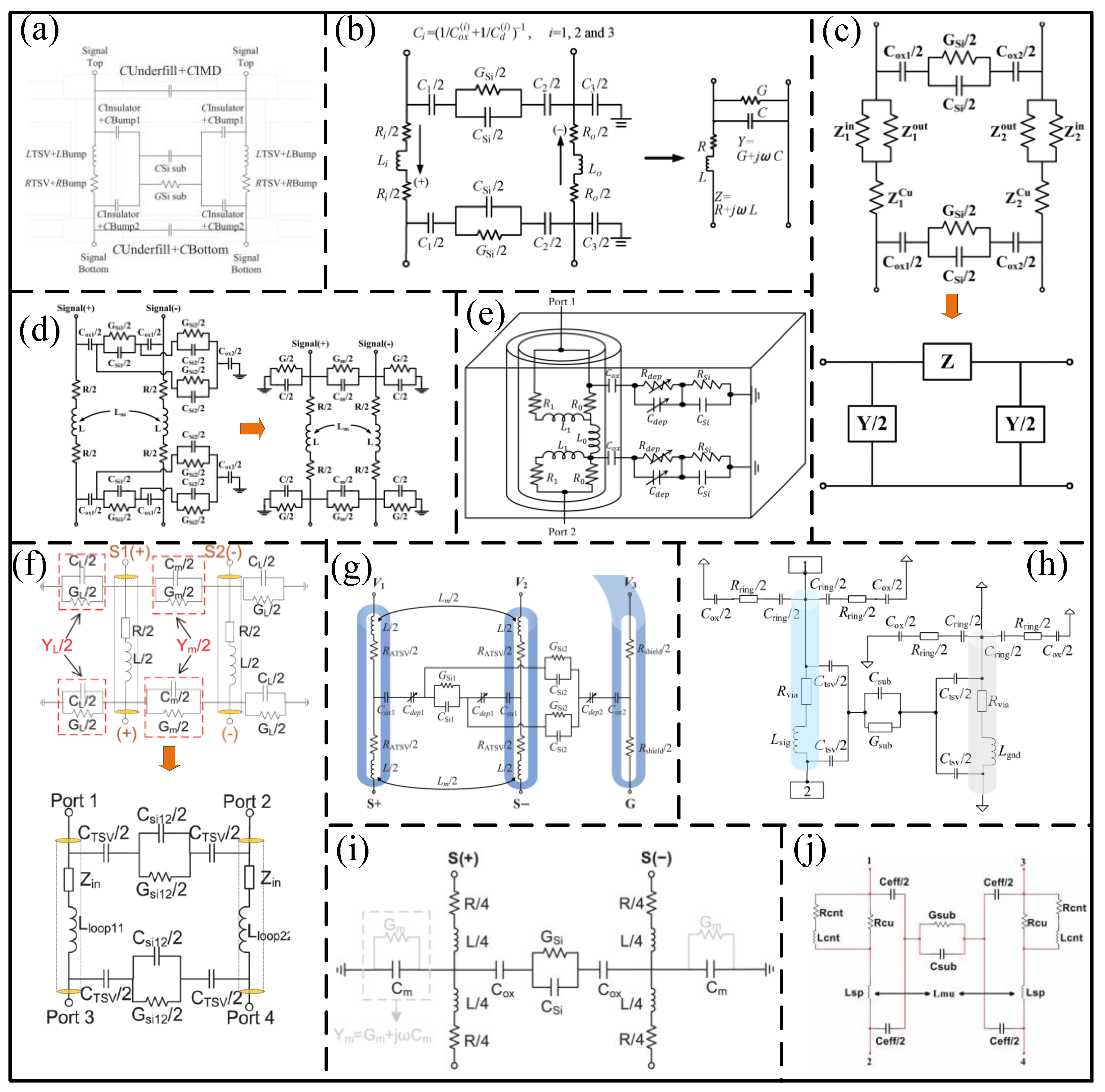
2.1. Lumped Parameter Model-Based Design

Generally, the closed-form expressions of the aggregate parameter model of the TSV are investigated based on the diameter of TSV, the height of TSV, the thickness of the insulation layer, the spacing from the ground TSV, the signal TSV, etc. Due to its simple structure, cylindrical TSV has been widely investigated. Savidis et al. [13] proposed the compute equations of the RLGC model of TSV based on the data fitting method. The numerical calculation results are compared with the simulation results, and the maximum errors of R, L and C are all less than 8%. The equivalent RLGC model of cylindrical TSV and the analytical equation of the lumped model parameter also has been proposed by Hu et al. [14], as shown in Figure 2a. The electrical characterization of TSV is analyzed in the frequency domain and time domain. In addition, the accurate electrical modeling of cylindrical TSV is proposed by Bandyopadhyay et al. [15] based on the metal-oxide-semiconductor (MOS) capacitance effects. Based on the Electroquasi-static theory and Bessel function, Xu et al. [16] established the RLGC model for TSVs valid from low- to high-frequency regimes, which consider the skin effect and MOS capacitance effect. Moreover, the coaxial TSV is proposed to decrease the crosstalk of the signal effectively. The outer metal layer of coaxial TSV has a shielding effect. Xu et al. [17] presented the RLGC empirical calculations expressions of coaxial TSV, which agree well with the full-wave extraction in coaxial TSV passive elements. Zhao et al. [18] proposed the equivalent lumped element circuit model of square and circular coaxial-TSV, as shown in Figure 2b. The parasitic capacitance, characteristic impedance and S parameters at different frequencies and temperatures are characterized and numerically compared. Lu et al. [19] proposed a wideband equivalent circuit model of coaxial annular TSV for 3D integrated circuits (ICs), as shown in Figure 2c. The closed-form expressions of RLGC are established based on the Bessel function, and the RLGC model is verified by a high-frequency simulator structure (HFSS). The maximum errors of R, L, G and C are 6.5%, 1.7%, 5.5% and 1.8%, respectively. Liang et al. [20] established the closed-form expression of resistance by solving the current continuity equation, and then the closed-form expression of inductance was established based on the Biot-Savart law. The maximum errors of resistance and inductance are 2% and 5%, respectively. Lu et al. [21] proposed the equivalent circuit model of shield differential TSVs in 3D IC, as shown in Figure 2d. The equivalent model is verified by 3D full-wave field solver HFSS, and the simulation results show that the equivalent model has a high accuracy during the range of 100 GHz. The high-frequency electromagnetic characteristics of differential impedance and insertion loss are analyzed. Salah et al. [22] proposed an equivalent lumped element model based on the physical size and material properties of TSV, as shown in Figure 2e. The closed-form expressions for R, L and C are introduced. The simulation results show that the maximum errors are all less than 6%. Qu et al. [23] established the equivalent model of differential TSV pair in 3D IC, as shown in Figure 2f. The computation results based on the equivalent are verified by HFSS in a wide frequency range. Fu et al. [24] proposed a shielded differential annular TSV and established the equivalent circuit model, as shown in Figure 2g. The simulation results show that the keep-out zone can be reduced without decreasing performance. Su et al. [25] propose a novel TSV that can be used to suppress the substrate noise. The equivalent RLGC model is established, as shown in Figure 2h. The simulation results show that the errors of |S11| and |S21| are less than 3.3 dB and 0.05 dB, respectively. Furthermore, Hu et al. [26] proposed the differential multibit carbon nanotube (CNT) TSV and established the equivalent RLGC model, as presented in Figure 2i. Rao [27] investigated the electrical characteristics of taper TSV and established the equivalent circuit model of RLGC, as shown in Figure 2j. The return loss of tapered TSV displayed at 30 GHz is less than −20 dB, which is conducive to the high-frequency application of tapered TSV. Liu et al. [28] proposed the parasitic inductor model of ground–signal–ground taper TSV pair. The simulation results show that the error of the model is less than 8%. Alam et al. [29] assumed that the silicon substrate of TSV is a metal conductor to derive the closed-form expression of capacitance, but the effect of the depletion layer is not considered. Weerasekera et al. [30] established the RLC model of TSV based on the experiments fitting, which did not consider the thickness of the oxide layer and depletion zone. The simulation results show that the maximum error is less than 6%. Katti et al. [31] established a depletion layer capacitance model of TSV based on the depletion layer width and verified the model through numerical emulators. The maximum error is less than 3.52%. Cai et al. [32] derived the parasitic capacitance expression of TSV based on the depletion zone capacitance and oxide layer capacitance and analyzed the capacitance model in detail. The computation results are compared with the simulated results by Silvaco. The error between the mathematical model and the simulation results is 6.9%, while the error between the mathematical model and the measured results is 10.1%. The maximum errors of different RLGC models are presented in Table 1. and the lumped parameter closed-form expressions of different TSV for different conditions are shown in Table 2.

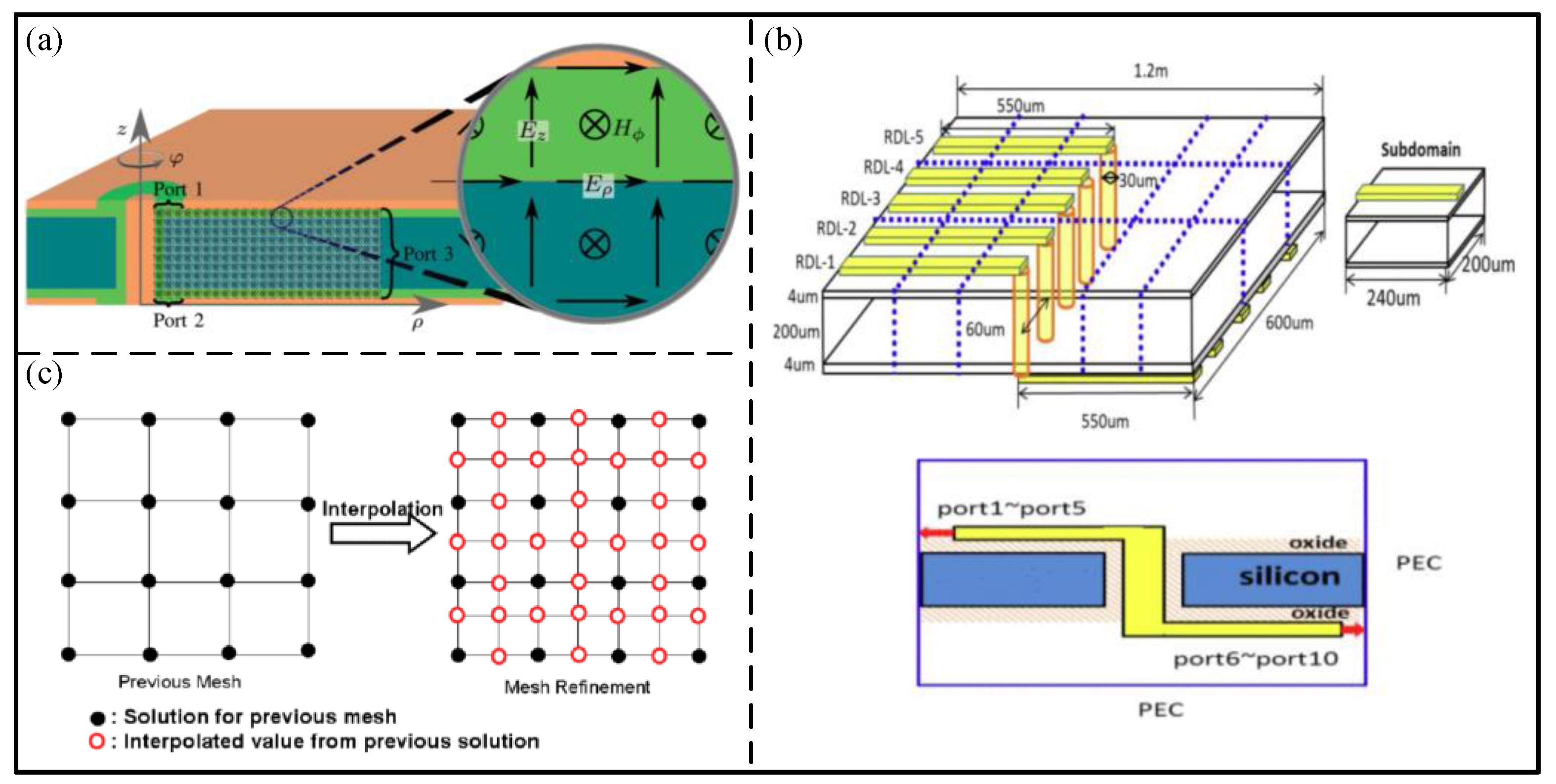
2.2. Numerical Computation Model-Based Design

Currently, the finite-difference method (FDM) model, finite element method (FEM) model, and finite volume method (FVM) model are the commonly used numerical computation model for 3D integrated systems. Although these numerical computation models are different in solving the electrical simulation performance of TSV, the Maxwell equation is the basic solution mode.
Under the framework of FDM, the problem domain is divided into a difference grid, and the problem domain is replaced by a finite number of network nodes. The FDM is approximately solved by the difference quotient of the function values on the grid nodes through the Taylor series expansion method. It has the advantages of perfect theory, applicable to various precision and easy parallel calculations. The disadvantages are that it is very complicated to deal with irregular areas, and a little mistake will cause a great error. Based on the FDM, Dahl et al. [38] used the rectangular grid to conduct near-field modeling of cylindrical TSV, as shown in Figure 3a. The sparse matrix can be obtained by dispersing Maxwell’s equations, and the impedance characteristics of TSV can be accurately further obtained through the sparse matrix. Xie et al. [39] proposed an efficient method for modeling signal paths with TSV in silicon interposer for a 3D integrated system, as shown in Figure 3b. The established model can accurately compute the parasitic effects of multiple transmission lines. Huang et al. [40] established the MOS capacitance model of TSV based on the FDM. The point distribution of the insulation layer and depletion layer can be obtained by only one iteration through the FDM.
The FEM is developed by the variational principle and weighted residual method. The basic strategy for solving the FEM is to divide the problem into a finite number of discretized elements. The appropriate nodes are selected as the interpolation points of the problem function to solve the differential equation in each element. Due to its high precision, the FEM has been widely used in the 3D integrated system. Whether the equivalent circuit model proposed by Kim et al. [21] or the cylindrical mode basis function proposed by Han et al. [41] is used to calculate the electrical characteristics of TSV, the R, C and L equations of TSV derived by Savidis et al. [13] are based on the FEM. The computation results of FEM are used as accurate solutions to validate these models and methods.
Figure 3. (a) Cut through the considered structure with finite-difference frequency domain grid for near-field modeling (Reprinted from [37], Copyright 2015, with permission from IEEE); (b) Five RDL–TSV–RDL transition structure and the cross-sectional view. (Reprinted from [38], Copyright 2014, with permission from IEEE); (c) Mesh refinement and interpolation. (Reprinted from [42], Copyright 2010, with permission from IEEE).
Symmetry 15 00418 g003
The FVM is used to divide the solution domain into a number of unrelated small volumes and connect them together through grid points. The interpolation function of the FVM is only used to compute the integral of a small volume, which makes it possible to use different interpolation functions for different terms in the differential equation. Based on the FVM, Xie et al. [42] proposed a non-uniform grid to calculate the voltage drop of a 3D power distribution network, as shown in Figure 3c. The effects of temperature on material properties and the relationship between resistivity and position are considered in the differential equation. Xu et al. [43] proposed an electromagnetic field semiconductor coupled solver for the investigation of 3D IC. Under the framework of the solver, the FVM is used to deal with the full wave effects and semiconductor effects of 3D IC.

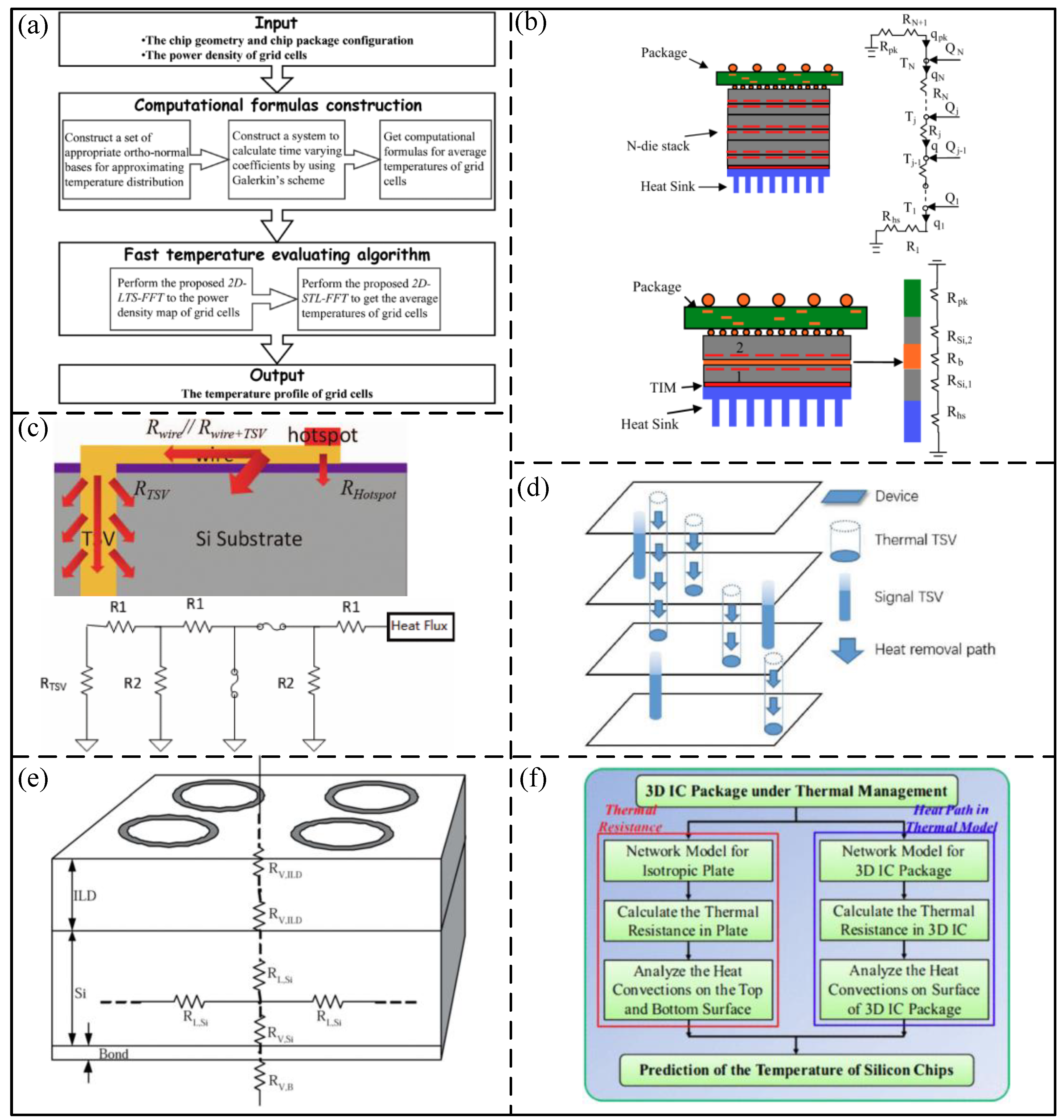
3. Thermal Simulation Design of TSV in 3D Integrated System

Because the stacking of multiple chips will increase the power density and reduce the cooling efficiency of the 3D integrated system, the thermal problem of the 3D integrated system becomes extremely serious [44,45,46,47]. In the thermal simulation design of TSV in a 3D integrated system, the critical design parameters based on the analytical model or numerical computation model are the design parameters of the TSV structure, the material parameters, the power consumption distribution between different layers, the operating frequency of the devices and circuits and the thermal impedance between chips. In addition, the key performance index for thermal simulation design is the peak temperature. In order to analyze the errors of the analytical model, the results of the analytical model are usually compared with the FEM-based numerical computation model. The path length and thermal resistance of the chips to the heat sink are increased. In addition, the local hot spots are aggregated to form volume hot spots by the stacked power density. With the increase in integration density, the temperature of the integrated system is constantly rising, and the performance, reliability and service life of the integrated system are greatly reduced. In order to predict and control the temperature of the 3D integrated system, the thermal performance of the 3D integrated is investigated and analyzed. The effective cooling method is very significant for the thermal management of 3D integrated systems. Currently, the analytical model and numerical computation model are mainly used to investigate the thermal problem of 3D integrated systems.

3.1. Analytical Model-Based Design

Based on Green’s function, Zhan et al. [48] proposed an analytical thermal algorithm for IC, which can compute the steady-state temperature of the whole chip according to different precision requirements. Huang et al. [49] improved the analytical thermal algorithm through generalized integral transformation, which has a faster computation speed than the algorithm derived by Green’s function. The flowchart is shown in Figure 4a. The maximum error is 0.3576%. In addition, Jain et al. [50] simplified the 3D integrated system into a 1D thermal resistance model, as shown in Figure 4b. Although the developed method can quickly compute the heat distribution of a 3D integrated system, the temperature measurement of each layer is not particularly accurate. Based on the TSV structure, Pi et al. [51] proposed a simplified calculation method of thermal diffusion resistance, as shown in Figure 4c. The FEM simulation is adopted to verify its accuracy. Based on the thermal resistance model and graph theory, Zhao et al. [52] established an overall multi-modal theoretical model with minimum cost and calculated the optimal layout of TSV through multi-level algorithms, as shown in Figure 4d. Based on the longitudinal heat transfer characteristics of TSV, Ayala et al. [53] established the thermal resistance model in the 3D integrated system. Liu et al. [54] proposed a side thermal resistance model of TSV based on the copper structure and oxide layer, as shown in Figure 4e. Lan et al. [55] established a comprehensive thermal analytic flowchart based on the thermal resistance model and 3D encapsulated network model, as shown in Figure 4f. Although the analytical method is fast in calculation and simple in modeling, its constraint is too strong. Generally, it can solve the steady state and simple 3D thermal model, and its accuracy is relatively poor.

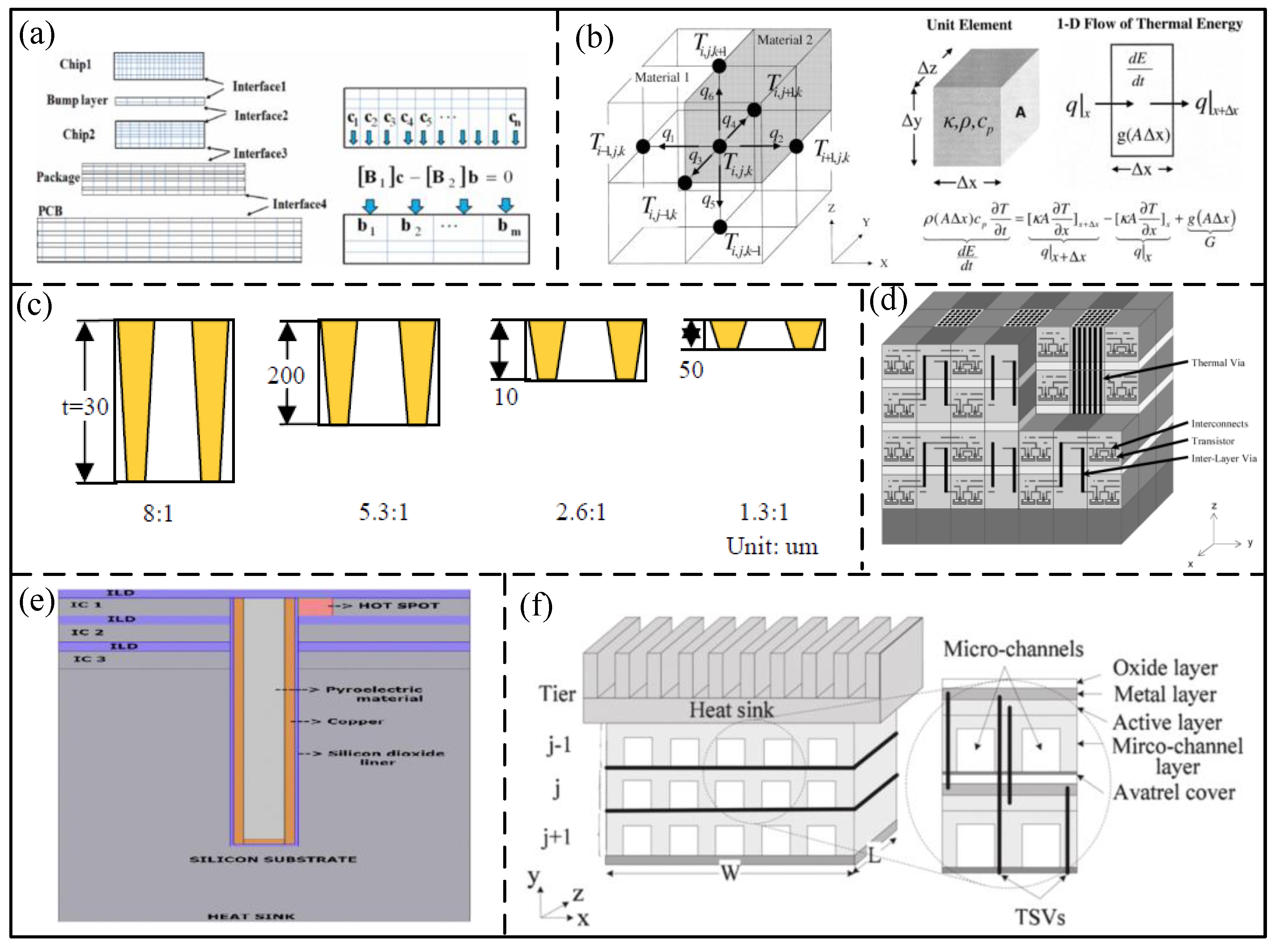
3.2. Numerical Computation Model-Based Design

Compared with the analytical model, the applicability of the numerical computation model is more general. This is because the numerical computation model can accurately solve the thermal problem of each part of the 3D integrated system, and the temperature change over time in the integrated system can also be accurately reflected. However, greater memory consumption and computing time are required. Zhu et al. [56] computed the heat conduction equation by FDM. The temperature matrix is computed by the minimum residual method and symmetric continuous overrelaxation pretreatment. Based on the FDM, Kuo et al. [57] investigated the thermal characteristics of system-level packages TSV. Xie et al. [58] investigated the transient thermal characteristics of the 3D integrated system based on the FEM and non-conformal domain decomposition method, as shown in Figure 5a. Based on the alternating implicit characteristics of unconditional steady-state, Wang et al. [59,60] evaluated the transient thermal characteristics of 3D chips combined with FEM, as shown in Figure 5b.
Due to high simulation accuracy, FEM has been widely used for the computing of 3D integrated systems. Based on the FEM, Fu et al. [61] proposed a triangular layout method of TSV. The thermal dissipation capacity of the TSV array is improved without increasing the occupied area; thus, the thermal performance of a 3D integrated system can be improved. The simulation results show that the average temperature and peak temperature are reduced by 0.22% and 1.69%, respectively, during vertical heat dissipation. The temperature is reduced by 0.10% for lateral heat transfer. Based on the FEM, Hoe et al. [62] improved the thermal conductivity at the connection points by adjusting the physical size of TSV; thus, the thermal performance of the 3D integrated system can be optimized, as shown in Figure 5c. Todri et al. [63] improved the integrity of the power supply and reduced the peak temperature by changing the physical form of TSV. However, this has a very limited impact on the heat dissipation efficiency of 3D integrated systems by improving the physical performance of TSV and its arrangement rule. In order to improve the heat conduction ability between layers and reduce the temperature of hot spots as soon as possible, Chiang et al. [64] proposed the concept of thermal TSV (TTSV). The TTSV is only used for interlayer heat conduction, and the diameter is much larger than the signal TSV. Goplen et al. [65] applied TTSV in 3D IC, as shown in Figure 5d. The TTSV is added to a specific area to adjust the effective thermal conductivity of 3D IC. The simulation results show that the proposed method can reduce the peak temperature by more than 57%. Singh et al. [66] performed a complete analysis of a single TTSV. When the TTSV is inserted at the hot spot of the chip, its temperature can be reduced by 62 °C. Wang et al. [67] proposed a high-efficiency design method of TSV array for thermal management of a 3D integrated system based on the FEM and equivalent thermal conductivity model. The simulation results show that the thermal distribution of the 3D integrated system is homogeneous. Based on the principle of the thermoelectric effect, Gagan et al. [68] proposed a novel TSV, as shown in Figure 5e. The novel TSV can be used to absorb heat and also serves to transport signals. In addition, Singh et al. [69] improved the heat dissipation performance by using CNT instead of traditional copper. Based on the FEM, Shi et al. [70] increased the thermal conductivity between the layers through combined the micro-channel with the TSV heat dissipation method, as shown in Figure 5f. The experiment results show that the developed method reduced the temperature by about 40% compared with the simple use of TSV, which made a great contribution to promoting the heat dissipation of the 3D integrated system by micro-channel.
Figure 5. (a) Non-conformal gridding of 3D system into domains and heat flow continuity illustration. (Reprinted from [58], Copyright 2012, with permission from IEEE); (b) Conservation of energy and the heat conduction equation. (Reprinted from [60], Copyright 2003, with permission from IEEE); (c) TSV geometry for different aspect ratios. (Reprinted from [62], Copyright 2009, with permission from IEEE); (d) Cutaway showing transistors and interconnects based on TSV. (Reprinted from [63], Copyright 2006, with permission from IEEE); (e) The schematic of the simulated 3D stack with TTSV (Reprinted from [68], Copyright 2015, with permission from IEEE); (f) Stacked 3D integrated system with micro-channels and TSVs. (Reprinted from [70], Copyright 2012, with permission from IEEE).
Symmetry 15 00418 g005

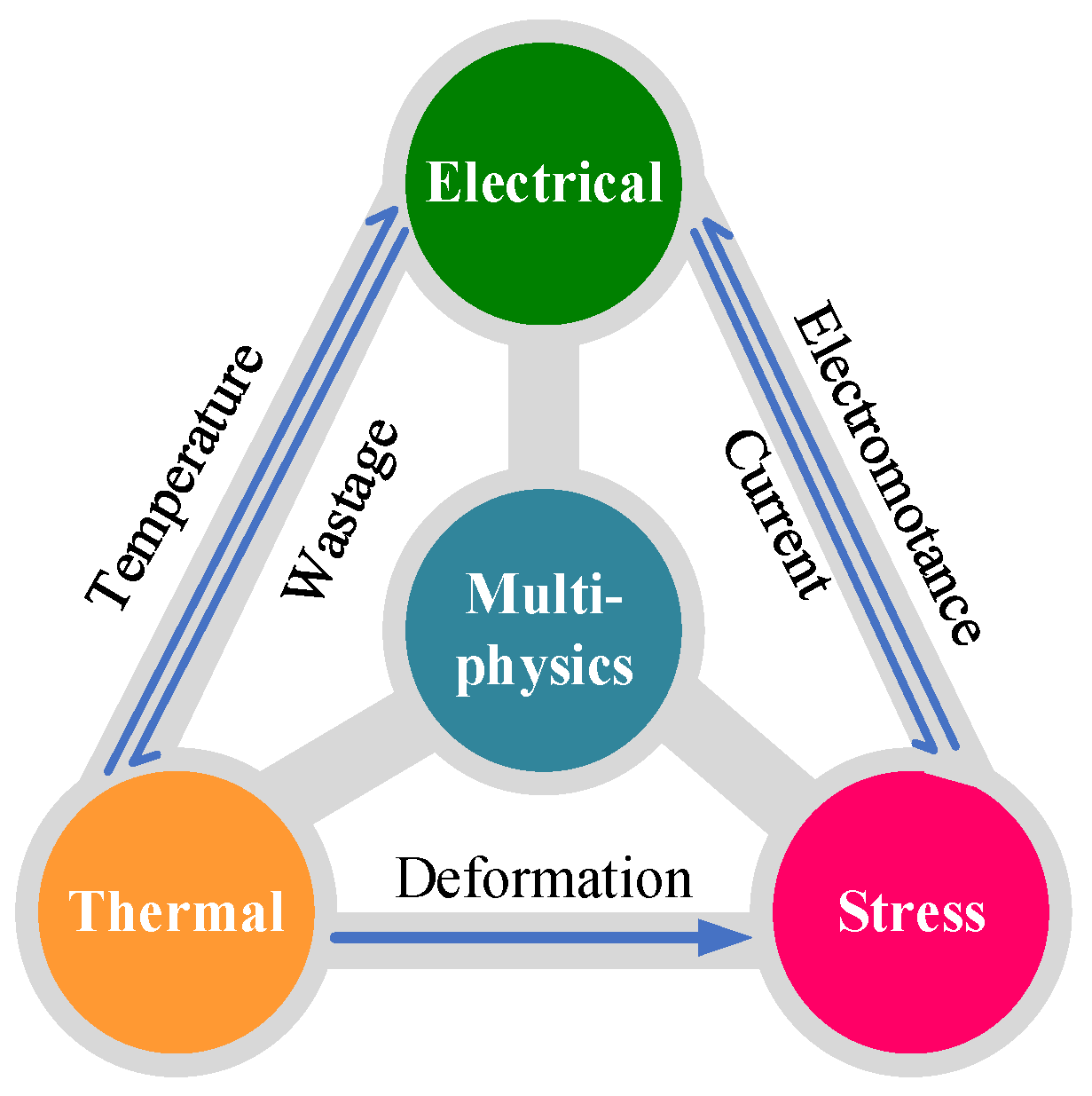
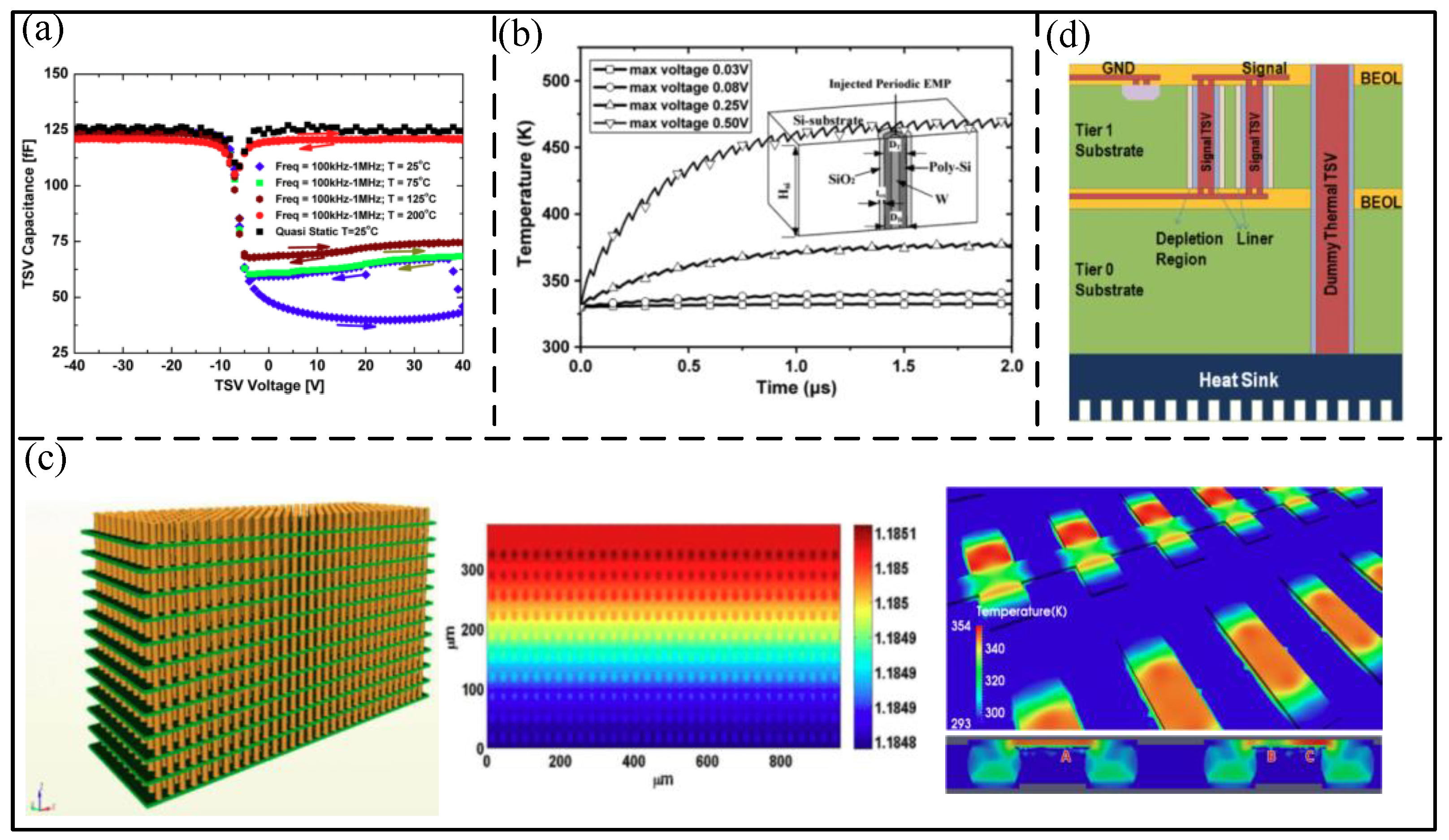
4. Multi-Physics Co-Simulation Design of TSV in 3D Integrated System

The unification of computing, electrical, physical, thermal and reliability aspects of an integrated system is called co-simulation design. Due to the lack of understanding of cross-domain interactions and their impacts on the feasibility region of the architectural design space, the independent optimization and design of each aspect lead to sub-optimal designs. Although the cooperative design strategy is becoming more and more necessary for 3D integrated systems, the high reliability of 3D integrated systems is becoming even more critical. The interlayer coupling with the system architecture and a higher degree of connectivity between components increases the independence between physical design parameters, architectural parameters, performance, hotspot distribution, power and reliability. The embedded TSV greatly influences the former parameters. The 3D integrated system extends the design space by stacking integrated chips in the vertical direction. When the system is operated, the signal input generates Joule heat, which brings various temperatures and affects its electrical parameters, silicon conductivity, thermal conductivity, etc. Meantime, due to the differences in CTE between materials, temperature changes generate thermal stress. The band gap width, carrier mobility and electrical parameters can be affected by the thermal stress. Therefore, it is necessary to develop the multi-physics co-simulation design of TSV in a 3D integrated system.

4.1. Thermal Stress Coupling Simulation Design

Because of the difference in CTE between the metal-filled TSV and the materials of the nearby structure, the thermal stress is generated after annealing and other manufacturing processes. Under the effects of thermal stress, the TSV is extruded and leads to the protrusion at both ends of the filled metal and the separation of the filled metal from the side wall. When the thermal stress is too large, the device will be destroyed. The band gap width and carrier mobility can be affected by thermal stress. Based on the reported work, 100 MPa of stress can change more than 7% of carrier mobility. Therefore, it is necessary to investigate the stress distribution evolution of TSV structure under thermal load. The investigation on the thermo-stress properties of TSV-based 3D integrated systems mainly focuses on the establishment of a thermal stress model, stress damage prediction and detection.
Generally, the thermal stress of cylindrical TSV has been investigated in the early stage, and the analytical model of the thermal stress introduced in silicon wafers has been established [71]. As shown in Figure 6a, the TSV is filled with copper, which causes large thermal stress. Then, the thermal stress is optimized based on the various TSV structures. Because the copper ring is used in the annular TSV [72], the thermal stress is much smaller than the cylindrical TSV filled with copper, as shown in Figure 6b. Based on the FEM, Wang et al. [73] proposed an analytical model of strain and stress for annular TSV. The simulation results show that the maximum average errors of strain and stress analytical models are 6.6% and 6.8%, respectively. Based on the FEM and stress analytical method, Lu et al. [74] investigated the thermal stress of TSV interconnect. The stress distribution of a single TSV is investigated by analytical method, and the stress interaction between the TSV arrays is further deduced based on the principle of linear superposition. The stress intensity factor on a radial crack is computed for TSV lines under 175 °C of thermal load. The effects of the TSV pitch on thermal stress are also investigated, as shown in Figure 6c. Due to the complex structure and large radius, the thermal stress problem of coaxial TSV [75] is more serious while improving the electrical characteristics. However, the coaxial annular TSV [76] is combined the superior thermal–mechanical characteristic of the annular TSV with the excellent electrical characteristic of the coaxial TSV, which reduces the thermal stress introduced in the silicon wafer on the premise of ensuring the superior electrical characteristic. The architecture and simulation results are shown in Figure 6d. In addition, Feng et al. [77] proposed an annular trench isolated TSV by adding a layer of silicon annular between the copper and insulation layers. The thermal stress generation point is moved from the boundary of TSV to the boundary of the silicon annular, and the thermal stress in the silicon substrate is reduced, as shown in Figure 6e. Since thermal stress is the main reason for device failure, the investigation of the effect of permutation on failure has a guiding significance for the design of the TSV array. Ryu et al. [78] investigated the effects of thermal stress on carrier mobility and keep-out zone by focusing on the stress characteristics near the surface where the electronics are located. Liu et al. [79] investigated the effect of copper column expansion of TSV on the stress of the redistribution layer, as shown in Figure 6f. The results show that the copper column protrusion tends to occur at the top edge of the TSV orifice under high thermal load, which leads to dielectric layer cracking and interface separation. The further results show that reducing the diameter and height of TSV is beneficial to reduce the influence of stress on the redistribution layer. Dong et al. [80] established a thermal stress analysis model of TSV and investigated the effects of TSV radius, the thickness of Cu diffusion barrier and the material on the thermal stress based on the FEM. The simulation results show that the error between the FEM model and the analysis model is 2%. Dequivre et al. [81] analyzed the TSV model and obtained its stress distribution gradient. The analysis is verified by the X-ray diffraction experiment, and the results show that the medium layer fracture is the main mechanism of device failure. Based on the internal stress distribution diagram of TSV under different thermal loads by using the electron backscattering diffraction method, Heryanto et al. [82] counted the height of TSV deformation at 250, 300, 350, 400 and 450 °C, which has reference significance for improving the high-temperature process. Based on the micro-infrared photoelasticity system with a thermal loading function, Su et al. [83] analyzed the stress of TSV. Yoo et al. [84] demonstrated the characterization of silicon stress near copper-filled TSV by using high-resolution micro-Raman spectroscopy and investigated the stress changes of TSV with different diameters, depth-to-width ratios and spacing distributions.
Based on the different heating rates, Zhao et al. [85] investigated the copper deformation behaviors of TSV, such as the invasion and protrusion of TSV copper. The results of Raman spectrums show that the changes in stress distribution are related to the copper deformation behavior. In the area near the Cu via, Cu protrusion behavior might aggravate the stress in Si obtained from the Raman measurement, while Cu intrusion might alleviate the stress. Based on the FEM, Zhang et al. [86] proposed a general method to predict the thermal distribution and stress distribution of the TSV array in a 3D integrated system. The individual and comprehensive effects of the parameters of the TSV array (TSV height, diameter and spacing etc.) on the thermal and stress of a 3D integrated system are predicted by the proposed method.
The thermal stress reliability of TSV is the main factor of device failure. Due to the large difference in the CTE between materials, the thermal stress is relatively high. Therefore, the effective way to reduce the thermal stress of a 3D integrated system is reducing the difference of CTE between materials to achieve the improvement of reliability.

4.2. Electro-Thermal Coupling Simulation Design

With the increase of integration density, the self-heating effect of interconnect has become an inevitable problem in 3D integrated systems. Therefore, a unified, standardized and systematic study on the electro-thermal coupling problem of TSV in a 3D integrated system was conducted. Wang et al. [87] investigated the effects of temperature on the parasitic resistance and capacitance of TSV through combined the properties of copper with the equivalent circuit model. Subsequently, Zhao et al. [88] extended the theory to coaxial TSV on this basis and analyzed the parasitic effect in detail. In addition, Katti et al. [89] verified the effects of temperature on TSV parasitic parameters based on experiments, and the results are shown in Figure 7a. Wang et al. [90] analyzed the thermal distribution and electric field distribution based on the FEM, and the electro-thermal characteristic is investigated by changing the amplitude of voltage and the thickness of the TSV oxide layer, as shown in Figure 7b. Based on the FEM, Lu et al. [91,92,93] investigated the influence of steady-state temperature distribution, DC voltage drop and high-frequency S parameter in electro-thermal coupling TSV array and power transmission networks. The instantaneous process is obtained, as shown in Figure 7c. Sai et al. [94] established a nonlinear electro-thermal delay model to investigate the TSV-based 3D integrated system, as shown in Figure 7d. The concept of virtual TSV is proposed to balance the temperature and stress gradient, and it is demonstrated that the clock shift is reduced by an average of 61.3% based on the proposed model. Based on the principle of heat–electricity analogy, Jiang et al. [95] analogized thermal to electrical to realize the steady-state thermal analysis of large-scale interconnect structures by using electrical simulation software, as shown in Figure 7e. In addition, the advantages and limitations of the analytical model, FDM, FEM and FVM are presented in Table 3.

5. Conclusions

The development and progress of multi-physics simulation design for TSV-based 3D integrated systems are reviewed in this paper. The highly reliable 3D integrated system is required to consider the electricity, thermal, stress and multi-physics coupling during the design and fabrication. With the development of 3D integrated systems, the application and innovation in many fields have made great progress, and the 3D integrated technology platforms with their own characteristics have been formed. The future development and perspectives of the 3D integrated system are summarized as follows:
(1)
Advanced integrated microsystems. The 3D integrated technology of imaging sensing is based on the route of imaging sensing chip and CMOS chip integration, using high-density TSV or inter-chip bonding technology, which lays a technical foundation for the development of computational and intelligent imaging in the future. The RF 3D integrated system has been widely applied in aerospace, aviation, ships, weapons, information technology, biology, medicine, industrial control, consumer electronics, etc. In addition, the Chiplet-based 3D integration technologies will be widely used in high-performance computing systems, high-reliability MEMS systems, mass memory systems, etc.
(2)
Crossed and reconfigurable architecture design technology. The 3D heterogeneous integration of the microsystem is focused on system-level packaging, and the crossed design from system to package is also required. In addition, the cost and lifetime of 3D wiring, multi-domain and multi-tools interactions are need to addressed for high-reliability 3D integrated microsystems. The reconfigurable technology can effectively improve the utilization efficiency of Chips and then improve the utilization range of 3D integrated microsystems. With the product development cycles continuing to shorten, collaborative design across multiple disciplines and domains such as circuit, structure, process and thermal design is required to achieve the 3D heterogeneous integrated microsystems.
(3)
Standardized and intelligent design technology. Standardized and intelligence are the design direction of 3D integrated microsystems. The standardized interconnection protocols can achieve the normalization and modularization of circuits in 3D integrated microsystems. In addition, intelligence refers to the application of the system to more scenarios and environments so that the degree of autonomy of the system is greatly enhanced. The application field of the system is significantly expanded, and the continuous innovation of the platform is promoted. Moreover, the intelligent optimization method can be used to improve the design efficiency of a 3D integrated system.

Author Contributions

Conceptualization, X.W. and D.C.; resources, X.W.; writing—original draft preparation, X.W. and D.C.; data curation, D.L.; writing—reviewing and editing, D.C. and D.L.; supervision, C.K. and Y.Y. All authors have read and agreed to the published version of the manuscript.

Funding

This research was funded by the Youth Talent Fund of Joint Fund of the Ministry of Education for Equipment Pre-Research (No: 8091B032138), Wuhu and Xidian University special fund for industry–university research cooperation (No: XWYCXY-012021008), the Cooperation Program of XDU-Chongqing IC Innovation Research Institute (No. CQIRI-2022CXY-Z01) and the Fundamental Research Funds for the Central Universities and the Innovation Fund of Xidian University.

Data Availability Statement

Not applicable.

Conflicts of Interest

The authors declare no conflict of interest.

References

  1. Beyne, E. The rise of the 3rd dimension for system integration. In Proceedings of the 2006 International Interconnect Technology Conference, Burlingame, CA, USA, 5–7 June 2006. [Google Scholar]
  2. Cheramy, S.; Charbonnier, J.; Henry, D.; Astier, A.; Chausse, P.; Neyret, M.; Brunet-Manquat, C.; Verrun, S.; Sillon, N.; Bonnot, L.; et al. 3D integration process flow for set-top box application: Description of technology and electrical results. In Proceedings of the 2009 European Microelectronics and Packaging Conference, Rimini, Italy, 15–18 June 2009. [Google Scholar]
  3. Vivet, P.; Guthmuller, E.; Thonnart, Y.; Pillonnet, G.; Moritz, G.; Miro-Panadès, I.; Fuguet, C.; Durupt, J.; Bernard, C.; Varreau, D.; et al. 2.3 A 220GOPS 96-Core Processor with 6 Chiplets 3D-Stacked on an Active Interposer Offering 0.6ns/mm Latency, 3Tb/s/mm2 Inter-Chiplet Interconnects and 156mW/mm2@ 82%-Peak-Efficiency DC-DC Converters. In Proceedings of the 2020 IEEE International Solid- State Circuits Conference-(ISSCC), San Francisco, CA, USA, 16–20 February 2020. [Google Scholar]
  4. Pawlowski, J.T. Hybrid memory cube (HMC). In Proceedings of the 2011 IEEE Hot Chips 23 Symposium (HCS), Stanford, CA, USA, 17–19 August 2011. [Google Scholar]
  5. Erofeev, E.; Arykov, V.; Stepanenko, M.; Voevodin, A.; Kogai, A.; Kurikalov, V. 28 GHz Single-Chip Transmit RF Front-End MMIC for Multichannel 5G Wireless Communications. Symmetry 2020, 12, 1167. [Google Scholar] [CrossRef]
  6. Shim, W.; Yu, S. Technological Design of 3D NAND-Based Compute-in-Memory Architecture for GB-Scale Deep Neural Network. IEEE Electron Device Lett. 2021, 42, 160–163. [Google Scholar] [CrossRef]
  7. Topol, A.W.; La Tulipe, D.C.; Shi, L.; Frank, D.J.; Bernstein, K.; Steen, S.E.; Kumar, A.; Singco, G.U.; Young, A.M.; Guarini, K.W.; et al. Three-dimensional integrated circuits. IBM J. Res. Dev. 2006, 50, 491–506. [Google Scholar] [CrossRef]
  8. Dang, B.; Wright, S.L.; Andry, P.S.; Sprogis, E.J.; Tsang, C.K.; Interrante, M.J.; Webb, B.C.; Polastre, R.J.; Horton, R.R.; Patel, C.S.; et al. 3D chip stacking with C4 technology. IBM J. Res. Dev. 2008, 52, 599–609. [Google Scholar] [CrossRef]
  9. Deguchi, J.; Sugimura, T.; Nakatani, Y.; Fukushima, T.; Koyanagi, M. Quantitative Derivation and Evaluation of Wire Length Distribution in Three-Dimensional Integrated Circuits Using Simulated Quenching. Jpn. J. Appl. Phys. 2006, 45, 3260. [Google Scholar] [CrossRef]
  10. Qian, L.; Qian, K.; He, X.; Chu, Z.; Ye, Y.; Shi, G.; Xia, Y. Through-Silicon Via-Based Capacitor and Its Application in LDO Regulator Design. IEEE Trans. Very Large Scale Integr. Syst. 2019, 27, 1947–1951. [Google Scholar] [CrossRef]
  11. Qian, L.; Xia, Y.; He, X.; Qian, K.; Wang, J. Electrical Modeling and Characterization of Silicon-Core Coaxial Through-Silicon Vias in 3-D Integration. IEEE Trans. Compon. Packag. Manuf. Technol. 2018, 8, 1336–1343. [Google Scholar] [CrossRef]
  12. Qu, C.; Ding, R.; Liu, X.; Zhu, Z. Modeling and Optimization of Multiground TSVs for Signals Shield in 3-D ICs. IEEE Trans. Electromagn. Compat. 2017, 59, 461–467. [Google Scholar] [CrossRef]
  13. Savidis, I.; Alam, S.M.; Jain, A.; Pozder, S.; Jones, R.E.; Chatterjee, R. Electrical modeling and characterization of through-silicon vias (TSVs) for 3-D integrated circuits. Microelectron. J. 2010, 41, 9–16. [Google Scholar] [CrossRef]
  14. Hu, J.; Wang, L.; Jin, L.; JiangNan, H.Z. Electrical modeling and characterization of through silicon vias (TSV). In Proceedings of the 2012 International Conference on Microwave and Millimeter Wave Technology (ICMMT), Shenzhen, China, 5–8 May 2012. [Google Scholar]
  15. Bandyopadhyay, T.; Han, K.J.; Chung, D.; Chatterjee, R.; Swaminathan, M.; Tummala, R. Rigorous Electrical Modeling of Through Silicon Vias (TSVs) With MOS Capacitance Effects. IEEE Trans. Compon. Packag. Manuf. Technol. 2011, 1, 893–903. [Google Scholar] [CrossRef]
  16. Xu, C.; Li, H.; Suaya, R.; Banerjee, K. Compact AC Modeling and Performance Analysis of Through-Silicon Vias in 3-D ICs. IEEE Trans. Electron Devices 2010, 57, 3405–3417. [Google Scholar] [CrossRef]
  17. Xu, Z.; Lu, J.Q. Three-Dimensional Coaxial Through-Silicon-Via (TSV) Design. IEEE Electron Device Lett. 2012, 33, 1441–1443. [Google Scholar] [CrossRef]
  18. Zhao, W.S.; Yin, W.Y.; Wang, X.P.; Xu, X.L. Frequency- and Temperature-Dependent Modeling of Coaxial Through-Silicon Vias for 3-D ICs. IEEE Trans. Electron Devices 2011, 58, 3358–3368. [Google Scholar] [CrossRef]
  19. Lu, Q.; Zhu, Z.; Liu, Y.; Liu, X.; Yin, X. Wideband Electromagnetic Modeling of Coaxial-Annular Through-Silicon Vias. IEEE Trans. Electromagn. Compat. 2018, 60, 1915–1922. [Google Scholar] [CrossRef]
  20. Liang, Y.; Li, Y. Closed-Form Expressions for the Resistance and the Inductance of Different Profiles of Through-Silicon Vias. IEEE Electron Device Lett. 2011, 32, 393–395. [Google Scholar] [CrossRef]
  21. Lu, Q.; Zhu, Z.; Yang, Y.; Ding, R. Electrical Modeling and Characterization of Shield Differential Through-Silicon Vias. IEEE Trans. Electron Devices 2015, 62, 1544–1552. [Google Scholar]
  22. Salah, K.; Ragai, H.; Ismail, Y.; Rouby, A.E. Equivalent lumped element models for various n-port Through Silicon Vias networks. In Proceedings of the 16th Asia and South Pacific Design Automation Conference (ASP-DAC 2011), Yokohama, Japan, 25–28 January 2011. [Google Scholar]
  23. Qu, C.; Ding, R.; Zhu, Z. High-Frequency Electrical Modeling and Characterization of Differential TSVs for 3-D Integration Applications. IEEE Microw. Wirel. Compon. Lett. 2017, 27, 721–723. [Google Scholar] [CrossRef]
  24. Fu, K.; Zhao, W.S.; Wang, G.; Swaminathan, M. Modeling and Performance Analysis of Shielded Differential Annular Through-Silicon Via (SD-ATSV) for 3-D ICs. IEEE Access 2018, 6, 33238–33250. [Google Scholar] [CrossRef]
  25. Su, J.; Zhang, W.; Yao, C. Partial Coaxial Through-Silicon via for Suppressing the Substrate Noise in 3-Dimensional Integrated Circuit. IEEE Access 2019, 7, 98803–98810. [Google Scholar] [CrossRef]
  26. Hu, Q.H.; Zhao, W.S.; Fu, K.; Wang, G. Modeling and Characterization of Differential Multibit Carbon-Nanotube Through-Silicon Vias. IEEE Trans. Compon. Packag. Manuf. Technol. 2020, 10, 534–537. [Google Scholar] [CrossRef]
  27. Rao, M. Electrical Modeling and Characterization of Copper/Carbon Nanotubes in Tapered through Silicon Vias. In Proceedings of the 2017 30th International Conference on VLSI Design and 2017 16th International Conference on Embedded Systems (VLSID), Hyderabad, India, 7–11 January 2017. [Google Scholar]
  28. Liu, X.; Zhu, Z.; Yang, Y.; Ding, R. Parasitic Inductance of Non-Uniform Through-Silicon Vias (TSVs) for Microwave Applications. IEEE Microw. Wirel. Compon. Lett. 2015, 25, 424–426. [Google Scholar] [CrossRef]
  29. Alam, S.M.; Jones, R.E.; Rauf, S.; Chatterjee, R. Inter-Strata Connection Characteristics and Signal Transmission in Three-Dimensional (3D) Integration Technology. In Proceedings of the 8th International Symposium on Quality Electronic Design (ISQED’07), San Jose, CA, USA, 26–28 March 2007. [Google Scholar]
  30. Weerasekera, R.; Grange, M.; Pamunuwa, D.; Tenhunen, H.; Zheng, L.R. Compact modelling of Through-Silicon Vias (TSVs) in three-dimensional (3-D) integrated circuits. In Proceedings of the 2009 IEEE International Conference on 3D System Integration, San Francisco, CA, USA, 28–30 September 2009. [Google Scholar]
  31. Katti, G.; Stucchi, M.; De Meyer, K.; Dehaene, W. Electrical Modeling and Characterization of Through Silicon via for Three-Dimensional ICs. IEEE Trans. Electron Devices 2010, 57, 256–262. [Google Scholar] [CrossRef]
  32. Jueping, C.; Peng, J.; Lei, Y.; Yue, H.; Zan, L. Through-silicon via (TSV) capacitance modeling for 3D NoC energy consumption estimation. In Proceedings of the 2010 10th IEEE International Conference on Solid-State and Integrated Circuit Technology, Shanghai, China, 1–4 November 2010. [Google Scholar]
  33. Kim, J.; Pak, J.; Cho, J.; Song, E.; Cho, J.; Kim, H.; Song, T.; Lee, J.; Lee, H.; Park, K.; et al. High-Frequency Scalable Electrical Model and Analysis of a Through Silicon Via (TSV). IEEE Trans. Compon. Packag. Manuf. Technol. 2011, 1, 181–195. [Google Scholar]
  34. Savidis, I.; Friedman, E.G. Closed-Form Expressions of 3-D Via Resistance, Inductance, and Capacitance. IEEE Trans. Electron Devices 2009, 56, 1873–1881. [Google Scholar] [CrossRef]
  35. Nicollian, E.H.; Brews, J.R. MOS (Metal Oxide Semiconductor) Physics and Technology; John Wiley & Sons: Somerset, NJ, USA, 2002; p. 928. [Google Scholar]
  36. Liao, H.Y.; Chiou, H.K. RF Model and Verification of Through-Silicon Vias in Fully Integrated SiGe Power Amplifier. IEEE Electron Device Lett. 2011, 32, 809–811. [Google Scholar] [CrossRef]
  37. Kim, J.; Pak, J.; Cho, J.; Lee, J.; Lee, H.; Park, K.; Kim, J. Modeling and analysis of differential signal Through Silicon Via (TSV) in 3D IC. In Proceedings of the 2010 IEEE CPMT Symposium Japan, Tokyo, Japan, 24–26 August 2010. [Google Scholar]
  38. Dahl, D.; Duan, X.; Ndip, I.; Lang, K.D.; Schuster, C. Efficient Computation of Localized Fields for Through Silicon Via Modeling Up to 500 GHz. IEEE Trans. Compon. Packag. Manuf. Technol. 2015, 5, 1793–1801. [Google Scholar] [CrossRef]
  39. Xie, B.; Swaminathan, M. FDFD Modeling of Signal Paths With TSVs in Silicon Interposer. IEEE Trans. Compon. Packag. Manuf. Technol. 2014, 4, 708–717. [Google Scholar] [CrossRef]
  40. Huang, C.; Liu, S.; Zhu, J.; Tang, W.; Zhuang, W. A novel modeling of TSV MOS capacitance by finite difference method. In Proceedings of the 2014 15th International Conference on Electronic Packaging Technology, Chengdu, China, 12–15 August 2014. [Google Scholar]
  41. Han, K.J.; Swaminathan, M.; Bandyopadhyay, T. Electromagnetic Modeling of Through-Silicon Via (TSV) Interconnections Using Cylindrical Modal Basis Functions. IEEE Trans. Adv. Packag. 2010, 33, 804–817. [Google Scholar] [CrossRef]
  42. Xie, J.; Swaminathan, M. DC IR drop solver for large scale 3D power delivery networks. In Proceedings of the 19th Topical Meeting on Electrical Performance of Electronic Packaging and Systems, Austin, TX, USA, 25–27 October 2010. [Google Scholar]
  43. Xu, Y.; Yu, W.; Chen, Q.; Jiang, L.; Wong, N. Efficient variation-aware EM-semiconductor coupled solver for the TSV structures in 3D IC. In Proceedings of the 2012 Design, Automation & Test in Europe Conference & Exhibition (DATE), Dresden, Germany, 12–16 March 2012. [Google Scholar]
  44. Jain, P.; Zhou, P.; Kim, C.H.; Sapatnekar, S.S. Thermal and Power Delivery Challenges in 3D ICs. In Three Dimensional Integrated Circuit Design; Xie, Y., Cong, J., Sapatnekar, S., Eds.; Integrated Circuits and Systems; Springer: Boston, MA, USA, 2010. [Google Scholar]
  45. Kashfi, F.; Draper, J. Thermal sensor design for 3D ICs. In Proceedings of the 2012 IEEE 55th International Midwest Symposium on Circuits and Systems (MWSCAS), Boise, ID, USA, 5–8 August 2012. [Google Scholar]
  46. Choday, S.H.; Lu, C.; Raghunathan, V.; Roy, K. On-chip energy harvesting using thin-film thermoelectric materials. In Proceedings of the 29th IEEE Semiconductor Thermal Measurement and Management Symposium, San Jose, CA, USA, 17–21 March 2013. [Google Scholar]
  47. Bandyopadhyay, S.; Chandrakasan, A.P. Platform architecture for solar, thermal and vibration energy combining with MPPT and single inductor. In Proceedings of the 2011 Symposium on VLSI Circuits—Digest of Technical Papers, Kyoto, Japan, 15–17 June 2011. [Google Scholar]
  48. Zhan, Y.; Sapatnekar, S.S. High-Efficiency Green Function-Based Thermal Simulation Algorithms. IEEE Trans. Comput.-Aided Des. Integr. Circuits Syst. 2007, 26, 1661–1675. [Google Scholar] [CrossRef]
  49. Huang, P.Y.; Lee, Y.M. Full-Chip Thermal Analysis for the Early Design Stage via Generalized Integral Transforms. IEEE Trans. Very Large Scale Integr. Syst. 2009, 17, 613–626. [Google Scholar] [CrossRef]
  50. Jain, A.; Jones, R.E. Chatterjee, S. Pozder. Analytical and Numerical Modeling of the Thermal Performance of Three-Dimensional Integrated Circuits. IEEE Trans. Compon. Packag. Technol. 2010, 33, 56–63. [Google Scholar] [CrossRef]
  51. Pi, Y.; Wang, W.; Jin, Y. An accurate calculation method on thermal effectiveness of TSV and wire. In Proceedings of the 2016 IEEE 18th Electronics Packaging Technology Conference (EPTC), Singapore, 30 November–3 December 2016. [Google Scholar]
  52. Zhao, Y.; Hao, C.; Yoshimura, T. Thermal and Wirelength Optimization With TSV Assignment for 3-D-IC. IEEE Trans. Electron Devices 2019, 66, 625–632. [Google Scholar] [CrossRef]
  53. Ayala, J.L.; Sridhar, A.; Cuesta, D. Thermal modeling and analysis of 3D multi-processor chips. Integration 2010, 43, 327–341. [Google Scholar] [CrossRef]
  54. Liu, Z.; Swarup, S.; Tan, S.X.D.; Chen, H.B.; Wang, H. Compact Lateral Thermal Resistance Model of TSVs for Fast Finite-Difference Based Thermal Analysis of 3-D Stacked ICs. IEEE Trans. Comput.-Aided Des. Integr. Circuits Syst. 2014, 33, 1490–1502. [Google Scholar] [CrossRef]
  55. Lan, J.-S.; Wu, M.-L. An analytical model for thermal failure analysis of 3D IC packaging. In Proceedings of the 2014 15th International Conference on Thermal, Mechanical and Mulit-Physics Simulation and Experiments in Microelectronics and Microsystems (EuroSimE), Ghent, Belgium, 7–9 April 2014. [Google Scholar]
  56. Zhu, J.; Liu, Y.; Zhuang, W.; Tang, W. Fast thermal analysis of TSV-based 3D-ICs by GMRES with symmetric successive over-relaxation (SSOR) preconditioning. In Proceedings of the 2015 IEEE Electrical Design of Advanced Packaging and Systems Symposium (EDAPS), Seoul, Republic of Korea, 14–16 December 2015. [Google Scholar]
  57. Kuo, W.S.; Wang, M.; Chen, E.; Lai, J.Y.; Wang, Y.P. Thermal Investigations of 3D FCBGA Packages with TSV Technology. In Proceedings of the 2008 3rd International Microsystems, Packaging, Assembly & Circuits Technology Conference, Taipei, Taiwan, 22–24 October 2008. [Google Scholar]
  58. Xie, J.; Swaminathan, M. 3D transient thermal solver using non-conformal domain decomposition approach. In Proceedings of the 2012 IEEE/ACM International Conference on Computer-Aided Design (ICCAD), San Jose, CA, USA, 5–8 November 2012. [Google Scholar]
  59. Wang, T.-Y.; Chen, C.C.-P. 3-D Thermal-ADI: A linear-time chip level transient thermal simulator. IEEE Trans. Comput. Aided Des. Integr. Circuits Syst. 2002, 21, 1434–1445. [Google Scholar] [CrossRef]
  60. Wang, T.-Y.; Chen, C.C.P. Thermal-ADI—A linear-time chip-level dynamic thermal-simulation algorithm based on alternating-direction-implicit (ADI) method. IEEE Trans. Very Large Scale Integr. Syst. 2003, 11, 691–700. [Google Scholar] [CrossRef]
  61. Fu, J.; Hou, L.; Wang, J.; Lu, B.; Zhao, W.; Yang, Y. A novel thermal-aware structure of TSV cluster. In Proceedings of the 2015 28th IEEE International System-on-Chip Conference (SOCC), Beijing, China, 8–11 September 2015. [Google Scholar]
  62. Hoe, Y.Y.G.; Yue, T.G.; Damaruganath, P.; Chong, C.T.; Lau, J.H.; Xiaowu, Z.; Vaidyanathan, K. Effect of TSV interposer on the thermal performance of FCBGA package. In Proceedings of the 2009 11th Electronics Packaging Technology Conference, Singapore, 9–11 December 2009. [Google Scholar]
  63. Todri, A.; Kundu, S.; Girard, P.; Bosio, A.; Dilillo, L.; Virazel, A. A Study of Tapered 3-D TSVs for Power and Thermal Integrity. IEEE Trans. Very Large Scale Integr. Syst. 2013, 21, 306–319. [Google Scholar] [CrossRef]
  64. Chiang, T.-Y.; Banerjee, K.; Saraswat, K.C. Effect of via separation and low-k dielectric materials on the thermal characteristics of Cu interconnects. In Proceedings of the International Electron Devices Meeting 2000. Technical Digest. IEDM (Cat. No.00CH37138), San Francisco, CA, USA, 10–13 December 2000. [Google Scholar]
  65. Goplen, B.; Sapatnekar, S.S. Placement of thermal vias in 3-D ICs using various thermal objectives. IEEE Trans. Comput. Aided Des. Integr. Circuits Syst. 2006, 25, 692–709. [Google Scholar] [CrossRef]
  66. Singh, S.G.; Tan, C.S. Thermal mitigation using thermal through silicon via (TTSV) in 3-D ICs. In Proceedings of the 2009 4th International Microsystems, Packaging, Assembly and Circuits Technology Conference, Taipei, Taiwan, 21–23 October 2009. [Google Scholar]
  67. Wang, X.; Yang, Y.; Chen, D.; Li, D. A High-efficiency Design Method of TSV Array for Thermal Management of 3D Integrated System. IEEE Trans. Comput.-Aided Des. Integr. Circuits Syst. 2022; early access. [Google Scholar] [CrossRef]
  68. Gagan, G.C.; Singh, S.G.; Dutta, A. Optimized ttsv structure for heat mitigation and energy harvesting. In Proceedings of the 2014 12th IEEE International Conference on Solid-State and Integrated Circuit Technology (ICSICT), Guilin, China, 28–31 October 2014. [Google Scholar]
  69. Singh, S.; Panigrahi, A.K.; Singh, O.K.; Singh, S.G. Analysis of graphene and CNT based finned TTSV and spreaders for thermal management in 3D IC. In Proceedings of the 2016 IEEE International 3D Systems Integration Conference (3DIC), San Francisco, CA, USA, 8–11 November 2016. [Google Scholar]
  70. Shi, B.; Srivastava, A.; Bar-Cohen, A. Hybrid 3D-IC Cooling System Using Micro-fluidic Cooling and Thermal TSVs. In Proceedings of the 2012 IEEE Computer Society Annual Symposium on VLSI, Amherst, MA, USA, 19–21 August 2012. [Google Scholar]
  71. Jan, S.-R.; Chou, T.-P.; Yeh, C.-Y.; Liu, C.W.; Goldstein, R.V.; Gorodtsov, V.A.; Shushpannikov, P.S. A Compact Analytic Model of the Strain Field Induced by Through Silicon Vias. IEEE Trans. Electron Devices 2012, 59, 777–782. [Google Scholar] [CrossRef]
  72. Lu, K.H.; Ryu, S.-K.; Zhao, Q.; Zhang, X.; Im, J.; Huang, R.; Ho, P.S. Thermal stress induced delamination of through silicon vias in 3-D interconnects. In Proceedings of the 2010 Proceedings 60th Electronic Components and Technology Conference (ECTC), Las Vegas, NV, USA, 1–4 June 2010. [Google Scholar]
  73. Wang, F.; Zhu, Z.; Yang, Y.; Liu, X.; Ding, R. Analytical models for the thermal strain and stress induced by annular through-silicon-via (TSV). IEICE Electron. Express 2013, 10, 20130666. [Google Scholar] [CrossRef]
  74. Lu, K.H.; Zhang, X.; Ryu, S.K.; Im, J.; Huang, R.; Ho, P.S. Thermo-mechanical reliability of 3-D ICs containing through silicon vias. In Proceedings of the 2009 59th Electronic Components and Technology Conference, San Diego, CA, USA, 26–29 May 2009. [Google Scholar]
  75. Adamshick, S.; Coolbaugh, D.; Liehr, M. Feasibility of coaxial through silicon via 3D integration. Electron. Lett. 2013, 49, 1028–1030. [Google Scholar] [CrossRef]
  76. Wang, F.; Zhu, Z.; Yang, Y.; Yin, X.; Liu, X.; Ding, R. An Effective Approach of Reducing the Keep-Out-Zone Induced by Coaxial Through-Silicon-Via. IEEE Trans. Electron Devices 2014, 61, 2928–2934. [Google Scholar] [CrossRef]
  77. Feng, W.; Bui, T.T.; Watanabe, N.; Shimamoto, H.; Aoyagi, M.; Kikuchi, K. Fabrication and stress analysis of annular-trench-isolated TSV. Microelectron. Reliab. 2016, 63, 142–147. [Google Scholar] [CrossRef]
  78. Ryu, S.K.; Lu, K.H.; Zhang, X.; Im, J.H.; Ho, P.S.; Huang, R. Impact of Near-Surface Thermal Stresses on Interfacial Reliability of Through-Silicon Vias for 3-D Interconnects. IEEE Trans. Device Mater. Reliab. 2011, 11, 35–43. [Google Scholar] [CrossRef]
  79. Liu, X.; Thadesar, P.A.; Taylor, C.L.; Kunz, M.; Tamura, N.; Bakir, M.S.; Sitaraman, S.K. Experimental Stress Characterization and Numerical Simulation for Copper Pumping Analysis of Through-Silicon Vias. IEEE Trans. Compon. Packag. Manuf. Technol. 2016, 6, 993–999. [Google Scholar] [CrossRef]
  80. Dong, G.; Shi, T.; Zhao, Y.-B.; Yang, Y.-T. An analytical model of thermal mechanical stress induced by through silicon via. Chinese Phys. B 2015, 24, 5. [Google Scholar] [CrossRef]
  81. Dequivre, T.; Kolhatkar, G.; Youssef, A.; Le, X.T.; Brisard, G.M.; Ruediger, A.; Charlebois, S.A. Wet Metallization of High Aspect Ratio TSV Using Electrografted Polymer Insulator to Suppress Residual Stress in Silicon. IEEE Trans. Device Mater. Reliab. 2017, 17, 514–521. [Google Scholar] [CrossRef]
  82. Heryanto, A.; Putra, W.N.; Trigg, A.D.; Gao, S.; Kwon, W.; Che, F.; Ang, X.; Wei, J.; Made, R.; Gan, C.; et al. Effect of Copper TSV Annealing on Via Protrusion for TSV Wafer Fabrication. J. Electron. Mater. 2012, 41, 2533–2542. [Google Scholar] [CrossRef]
  83. Su, F.; Lan, T.; Pan, X. Stress evaluation of Through-Silicon Vias using micro-infrared photoelasticity and finite element analysis. Opt. Lasers Eng. 2015, 74, 87–93. [Google Scholar] [CrossRef]
  84. Kim, J.H.; Han, S.M.J.; Yoo, W.S. Multiwavelength Raman characterization of silicon stress near through-silicon vias and its inline monitoring applications. J. Micro/Nanolithography MEMS MOEMS 2014, 13, 011205. [Google Scholar]
  85. Zhao, X.; Ma, L.; Wang, Y.; Guo, F. Effect of Thermal Mechanical Behaviors of Cu on Stress Distribution in Cu-Filled Through-Silicon Vias Under Heat Treatment. J. Electron. Mater. 2018, 47, 142–147. [Google Scholar] [CrossRef]
  86. Zhang, C.; Li, L. Characterization and Design of Through-Silicon Via Arrays in Three-Dimensional ICs Based on Thermomechanical Modeling. IEEE Trans. Electron Devices 2011, 58, 279–287. [Google Scholar] [CrossRef]
  87. Wang, X.P.; Zhao, W.; Yin, W.Y. Electrothermal modelling of through silicon via (TSV) interconnects. In Proceedings of the 2010 IEEE Electrical Design of Advanced Package & Systems Symposium, Singapore, 7–9 December 2010. [Google Scholar]
  88. Zhao, W.S.; Wang, X.P.; Xu, X.L.; Yin, W.Y. Electrothermal modeling of coaxial through silicon via (TSV) for three-dimensional ICs. In Proceedings of the 2010 IEEE Electrical Design of Advanced Package & Systems Symposium, Singapore, 7–9 December 2010. [Google Scholar]
  89. Katti, G.; Stucchi, M.; Velenis, D.; Soree, B.; De Meyer, K.; Dehaene, W. Temperature-Dependent Modeling and Characterization of Through-Silicon Via Capacitance. IEEE Electron Device Lett. 2011, 32, 563–565. [Google Scholar] [CrossRef]
  90. Wang, X.P.; Yin, W.Y.; He, S. Multiphysics Characterization of Transient Electrothermomechanical Responses of Through-Silicon Vias Applied With a Periodic Voltage Pulse. IEEE Trans. Electron Devices 2010, 57, 1382–1389. [Google Scholar] [CrossRef]
  91. Lu, T.; Jin, J.M. Electrical-Thermal Co-Simulation for DC IR-Drop Analysis of Large-Scale Power Delivery. IEEE Trans. Compon. Packag. Manuf. Technol. 2014, 4, 323–331. [Google Scholar] [CrossRef]
  92. Lu, T.; Jin, J.M. Thermal-Aware High-Frequency Characterization of Large-Scale Through-Silicon-Via Structures. IEEE Trans. Compon. Packag. Manuf. Technol. 2014, 4, 1015–1025. [Google Scholar] [CrossRef]
  93. Lu, T.; Jin, J.M. Transient Electrical-Thermal Analysis of 3-D Power Distribution Network With FETI-Enabled Parallel Computing. IEEE Trans. Compon. Packag. Manuf. Technol. 2014, 4, 1684–1695. [Google Scholar]
  94. Sai, M.P.D.; Yu, H.; Shang, Y.; Tan, C.S.; Lim, S.K. Reliable 3-D Clock-Tree Synthesis Considering Nonlinear Capacitive TSV Model With Electrical–Thermal–Mechanical Coupling. IEEE Trans. Comput.-Aided Des. Integr. Circuits Syst. 2013, 32, 1734–1747. [Google Scholar] [CrossRef]
  95. Jiang, L.; Xu, C.; Rubin, B.J.; Weger, A.J.; Deutsch, A.; Smith, H.; Caron, A.; Banerjee, K. A Thermal Simulation Process Based on Electrical Modeling for Complex Interconnect, Packaging, and 3DI Structures. IEEE Trans. Adv. Packag. 2010, 33, 777–786. [Google Scholar] [CrossRef]
Figure 1. Multi-physical field coupling relationship.
Symmetry 15 00418 g001
Figure 2. (a) Equivalent RLGC model of TSVs. (Reprinted from [14], Copyright 2012, with permission from IEEE); (b) Equivalent lumped-element circuit model and its simplified transmission-line model of the coaxial-TSV. (Reprinted from [18], Copyright 2011, with permission from IEEE); (c) Equivalent circuit model and its simplified model of coaxial annular TSVs. (Reprinted from [19], Copyright 2018, with permission from IEEE); (d) Equivalent circuit model and its simplified model of shield differential TSVs. (Reprinted from [21], Copyright 2015, with permission from IEEE); (e) The proposed lumped model for a TSV based on a single π structure. (Reprinted from [22], Copyright 2011, with permission from IEEE); (f) Simplified equivalent circuit model of differential TSVs and Equivalent circuit model of two signal TSVs. (Reprinted from [23], Copyright 2017, with permission from IEEE); (g) Equivalent circuit model of the shielded differentia annular TSV. (Reprinted from [24], Copyright 2018, with permission from IEEE); (h) Schematic of partial coaxial TSV and its equivalent circuit model. (Reprinted from [25], Copyright 2019, with permission from IEEE); (i) Schematic of the differential multibit CNT TSVs and its Equivalent circuit model. (Reprinted from [26], Copyright 2020, with permission from IEEE); (j) Equivalent RLGC circuit of CU/SWNTS filled tapered TSVs. (Reprinted from [27], Copyright 2017, with permission from IEEE).
Symmetry 15 00418 g002
Figure 4. (a) Executing flow of the proposed generalized integral transform-based thermal simulator. (Reprinted from [49], Copyright 2009, with permission from IEEE); (b) Thermal resistance network with multiple heat-generating junctions. (Reprinted from [50], Copyright 2009, with permission from IEEE); (c) Equivalent thermal resistance network. (Reprinted from [51], Copyright 2017, with permission from IEEE); (d) Heat dissipation path. (Reprinted from [52], Copyright 2018, with permission from IEEE); (e) Extending the proposed lateral model into more complicated TSV structures. (Reprinted from [54], Copyright 2014, with permission from IEEE); (f) Thermal analytic flowchart based on the thermal resistance model and 3D encapsulated network model. (Reprinted from [55], Copyright 2014, with permission from IEEE).
Symmetry 15 00418 g004
Figure 6. (a) Structure of the TSV filled with different materials, and the dent on TSV surface. (Reprinted from [71], Copyright 2012, with permission from IEEE); (b) The structure of annular TSV. (Reprinted from [72], Copyright 2010, with permission from IEEE); (c) Thermal stress around TSVs with various structures. (Reprinted from [74], Copyright 2009, with permission from IEEE); (d) Comparison of thermal stress results from analytical solution with FEM simulation for coaxial and coaxial annular TSVs. (Reprinted from [76], Copyright 2014, with permission from IEEE); (e) The von Mises stress distributions for annular-trench-isolated TSV, regular TSV and annular TSV at 125 °C. (Reprinted from [77], Copyright 2016, with permission from ELSEVIER). (f) CTE mismatch-induced stress in the TSV structure. (Reprinted from [79], Copyright 2016, with permission from IEEE).
Symmetry 15 00418 g006
Figure 7. (a) C−V characteristics of TSV at higher operating temperatures. (Reprinted from [86], Copyright 2011, with permission from IEEE); (b) Transient temperature responses of two single-layered H-shaped TSVs with a trapezoidal voltage pulse applied. (Reprinted from [87], Copyright 2010, with permission from IEEE); (c) The 3D structure, DC voltage drop and temperature distribution of TSV. (Reprinted from [88,89,90], Copyright 2014, with permission from IEEE); (d) Signal TSV in 3D IC and the virtual TSV. (Reprinted from [91], Copyright 2013, with permission from IEEE).
Symmetry 15 00418 g007
Table 1. Maximum errors of different RLGC model.
Ref.Maximum Errors
RLGC
Savidis et al. [13]8%8%8%8%
Lu et al. [19]6.5%1.7%5.5%1.8%
Liang et al. [20]2%5%--
Salah et al. [22]6%6%-6%
Liu et al. [28]-8%--
Weerasekera et al. [30]2%3%-6%
Katti et al. [31]---3.52%
Cai et al. [32]---10.1%
Table 2. Closed-form expressions for different TSV.
Closed-Form ExpressionsReference
R DC = ρ H TSV π r TSV 2 [32]
R DC = ρ H TSV π ( r 1 + H TSV r 2 ) [ 1 + 1 2 r 2 2 ] [20]
R AC = ρ H TSV π ( r TSV 2 ( r T S V δ ) 2 ) [33]
R AC = ρ ( 2 + r 2 2 ) 4 π r 2 δ ln ( 1 + 2 r 2 H TSV 2 r 1 δ ) [20]
L = μ 0 4 π [ 2 H TSV ln ( ( 2 H TSV + r T S V 2 + ( 2 H TSV ) 2 ) / r T S V ) + r T S V r T S V 2 + ( 2 H TSV ) 2 ] [31]
L = μ 0 α 2 π [ H TSV ln ( ( H TSV + r T S V 2 + H TSV 2 ) / r T S V ) + r T S V r T S V 2 + H TSV 2 + H TSV 4 ] [34]
L = μ 0 4 π [ 2 H TSV ( ( H TSV + r 1 2 + H T S V 2 ) / r 1 ) + 2 r 1 2 r 1 2 + H T S V 2 + 0.5 H TSV + 4 β H TSV ( H T S V 2 ( H TSV + r 1 ) ( r 1 2 + H T S V 2 r 1 ) ) ( r 1 2 + H T S V 2 H TSV ) ( 4 r 1 + β H TSV ) ] [20]
L = μ 0 2 π H TSV ln ( 1 + 2.84 H TSV / π r T S V ) [30]
L 21 = μ 0 α 2 π [ H TSV ln ( ( H TSV + p 2 + H TSV 2 ) / p ) + p p 2 + H TSV 2 ] [34]
L 21 = μ 0 2 π [ H TSV ln ( H TSV + p 2 + H TSV 2 p ) + p p 2 + H TSV 2 + 2 β H TSV ( H TSV 2 ( H TSV + p ) ( p 2 + H TSV 2 p ) ) ( p 2 + H TSV 2 H TSV ) ( 4 p + β H TSV ) ] [20]
C ox = ( ε 0 ε o x / t o x ) 2 π r TSV H TSV [35]
C ox = ε 0 ε o x ln ( ( r TSV + t o x ) / r TSV ) 2 π H TSV [36]
C = 63.34 H TSV ε 0 ln ( 1 + 5.26 H TSV / r TSV ) [30]
C dep = 2 π H TSV ε 0 ε s i ln ( ( r TSV + t o x + W dep ) / r TSV ) 1 V / V t h [22]
C dep = 2 π H TSV ε 0 ε s i ln ( ( r TSV + t o x + W dep ) / ( r TSV + t o x ) ) [31]
C S i = 0.5 π H TSV ε 0 ε s i α ( 8 n b c + 1 ) p r TSV ln ( ( r TSV + w b c ) / r TSV ) [22]
C S i = ε 0 ε s i 0.5 p + 2 r TSV + β 1 α 1 p H TSV [37]
G S i = σ s i 0.5 p + 2 r TSV + β 1 α 1 p H TSV [37]
G S i = 0.5 σ s i ( 8 n b c + 1 ) π H TSV ( α 1 p / r TSV ) ln ( ( r TSV + w bc ) / r TSV ) [37]
H TSV is the height of TSV, and r TSV is the radius of TSV. ρ represents the electrical resistivity. r 1 and r 2 are the bottom and top radius of taper TSV, respectively. δ represents the skin depth. μ 0 is the magnetic conductivity. α represents the fit coefficient. p is the spacing between the TSVs. ε 0 , ε o x and ε s i are the permittivity of vacuum, dielectric constant of oxide layer and dielectric constant of silicon, respectively. t o x is the thickness of oxide layer. W dep is the width of depletion layer. V is the impressed voltage, and V th is the threshold voltage. n b c is the coefficient of body contact, and w bc is the spacing of body contact. σ s i is the electrical conductivity of silicon.
Table 3. Advantages and limitations of analytical model, FDM, FEM and FVM.
ModelsAdvantagesLimitations
Analytical modelSimple and easy;
Low computational complexity;
High computing efficiency.
Limited parameters for analysis;
Low precision.
FDMTheoretical perfection;
Applicable to various accuracies;
Easy to compute in parallel.
Complicated dealing with irregular areas;
Poor adaptability to grids.
FEMHigh precision;
Multiple parameters for analysis;
Easier to handle irregular areas;
Easy to compute boundaries;
Good adaptability to grids.
Low computing efficiency;
High computational complexity;
High computational memory consumption.
FVMGood conservativeness;
Good adaptability to grids.
Complicated computing boundary;
High computational memory consumption;
Low simulation efficiency.
Disclaimer/Publisher’s Note: The statements, opinions and data contained in all publications are solely those of the individual author(s) and contributor(s) and not of MDPI and/or the editor(s). MDPI and/or the editor(s) disclaim responsibility for any injury to people or property resulting from any ideas, methods, instructions or products referred to in the content.

