Review

The CGEM-IT: An Upgrade for the BESIII Experiment

1
Institute of High Energy Physics, Chinese Academy of Sciences, Beijing 100049, China
2
INFN-Sezione di Ferrara, 44122 Ferrara, Italy
3
INFN-Sezione di Torino, 10125 Turin, Italy
4
Dipartimento di Fisica, Università di Torino, 10125 Turin, Italy
*
Author to whom correspondence should be addressed.
Symmetry 2022, 14(5), 905; https://doi.org/10.3390/sym14050905
Submission received: 28 March 2022 / Revised: 13 April 2022 / Accepted: 18 April 2022 / Published: 28 April 2022
(This article belongs to the Section Physics)

Abstract

:
The BESIII experiment has been collecting data since 2009 at the e + e collider BEPCII in Beijing, a charm- τ factory characterized by high statistics and high precision. The discovery of exotic charmonium-like states and the still open questions in low-energy QCD led to an extension of the experimental program, with several upgrades. This review focuses on the CGEM-IT, the innovative solution proposed to replace the current inner tracker, which is aging. It consists of three, co-axial, cylindrical triple-GEM detectors and will be the first cylindrical GEM operating inside a 1 T magnetic field with analogue readout. For this purpose, a dedicated mixed-signal ASIC for the readout of CGEM-IT signals and FPGA-based electronics for data processing have been developed. The simultaneous measurement of both ionization charge and time distribution enables three reconstruction algorithms, to cope with the asymmetry of the electron avalanche in the magnetic field and with non-orthogonal incident tracks. The CGEM-IT will not only restore the design efficiency but also improve the secondary vertex reconstruction and the radiation tolerance. The gas mixture and gain settings were chosen to optimize the position resolution to ∼130 µm in the transverse plane and better than 350 µm along the beam direction. This paper addresses the innovative aspects in terms of construction, readout, and software, employed to achieve the design goals as well as the experimental measurements performed during the development and commissioning of the CGEM-IT.
Keywords:
MPGD; GEM; CGEM; tracker; HEP

1. Introduction

The BEijing Spectrometer III (BESIII [1]) is the third evolution of the experiment placed at the interaction point of the Beijing Electron Positron Collider II (BEPCII), at the Institute of High Energy Physics (IHEP) of the Chinese Academy of Sciences in Beijing. BEPCII [2] is a multi-bunch e + e collider with a double-ring structure. The design luminosity of the accelerator is 10 33 cm 2 s 1 and the energy in the center of mass, which by design used to be in the range [2.0, 4.6] GeV, now has an upper limit of 4.95 GeV. Thanks to the accessible energy, BEPCII is a charm- τ factory and BESIII is a multipurpose spectrometer for precision and discovery physics in this energy regime.
The characteristics of the accelerator and of the detector have been carefully designed to make them a perfect tool to study the physics of the Standard Model at the charm- τ threshold, particularly the Quantum Chromo-Dynamics (QCD). This theory describes the interaction between quarks inside baryons and mesons and also predicts the existence of additional particles, with exotic structures, such as tetraquarks, pentaquarks, glueballs, hybrids, etc. [3].
BESIII plays a major role in the study of the QCD in the region of the charmonium and light hadrons. Moreover, since the discovery of the first X state, the X(3872), by Belle [4] and the first Y state, the Y(4260), by BaBar [5], BESIII has contributed to the definition of the scenario of these non-conventional hadrons, commonly called the X Y Z states. It confirmed the existence of the X(3872) [6] and it studied the Y states with the advantage of direct formation from e + e annihilation via a single virtual photon, being these 1 states. For example, while searching for the Y(4260), BESIII found that it is indeed a double structure [7], thanks to an order of magnitude better statistical precision. BESIII discovered the first confirmed Z state, the Z c (3900) [8] and the Z c (4020) [9]. Most recently it has found evidence of the first hidden-charm tetraquark candidate with non-zero strangeness, the Z c s (3985) [10]. The experiment can count on high precision measurements and on the high statistics of the data samples. For example, it has collected the world’s largest sample of J/ ψ events (10 billions) by 2019, from the direct production in electron-positron annihilation and holds the largest ψ ( 2 S ) and ψ ( 3770 ) data samples.

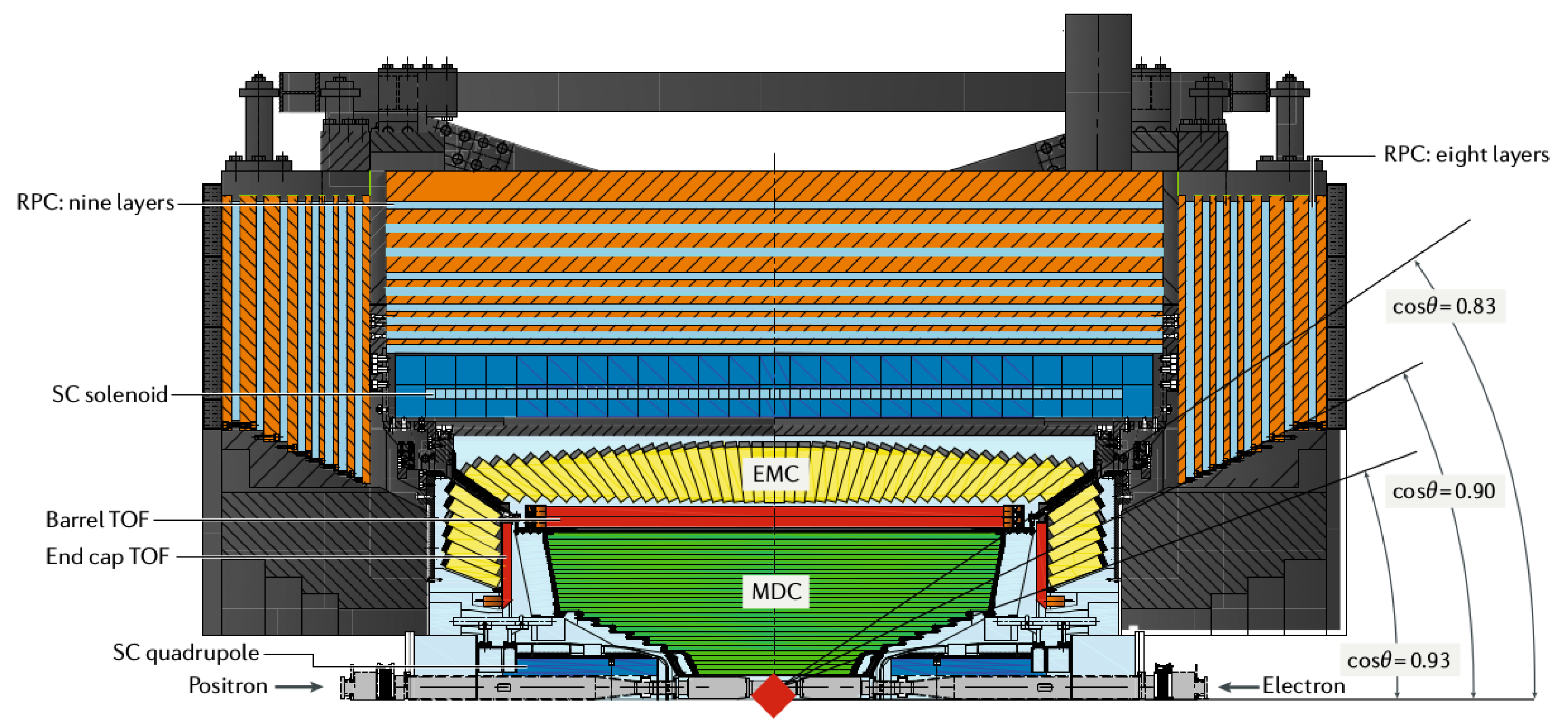
1.1. BESII and BEPCII

BESIII is designed to fulfill the physics and the technical requirements for a high-luminosity and multi-bunch collider. Details of the BESIII physics program can be found in the Yellow Book [11] and in the White Paper [12].
The BESIII layout is shown in Figure 1: it is composed of a set of detection systems and a solenoidal magnet that generates a 1 T magnetic field. The co-existing systems identify charged particle trajectories and reconstruct their momentum, measure the energy loss of both charged and neutral particles, and perform particle identification. The spectrometer has a cylindrical symmetry around the beryllium beam pipe of BEPCII. The innermost sub-system is an helium-based Main Drift Chamber (MDC) with a single wire resolution of 120 µm, a dE/dx better than 6% and a momentum resolution better than 0.5% for charged tracks with a momentum of 1 GeV/c. Outside the MDC, the Time-Of-Flight (TOF) system for particle identification is located. Its original design consists of two layers of plastic scintillator. Recent upgrades have introduced a multi-gap resistive plate chamber in the end-caps. The CsI(Tl) Electro-Magnetic Calorimeter (EMC) is placed between the TOF system and the Superconducting Solenoid Magnet (SSM). Its energy resolution is better than 2.5% and the position resolution is better than 6 mm for 1 GeV electrons and photons. The MUon Counter (MUC) is composed of nine layers of resistive plate chambers placed in the gaps between the steel plates of the flux return yoke. Their spatial resolution is better than 2 cm. The covered solid angle is Δ Ω / 4 π = 0.93, of which the azimuth angle is totally covered while the polar angle is limited between 21° and 159°. A detailed description of the detector can be found in [1].
BESIII was completed in 2008 and began taking physics data in 2009, after the BEPCII test runs. Due to the high radiation level during more than 10 years of data acquisition, some parts of the detector began to show aging problems. This issue led to some relevant upgrades. Also, the accelerator has been modified to improve its performance.
The upgrade of both the accelerating machine and the spectrometer grants 10 additional years of data taking, which will provide a contribution in various fields, such as the lepton flavor universality, the unitarity of the Cabibbo–Kobayashi–Maskawa (CKM) matrix, and the validity of lattice QCD. It will also enable the evaluation of the decay constants and the form factors by the study of leptonic and semileptonic decays of charmed particles. In particular, BESIII contributes with its high statistics samples and clean environment to the area of low energy, non-perturbative QCD [12].

1.2. BEPCII Upgrade

The accelerator has been running since 2008 and has reached its design luminosity of 10 33 cm 2 s 1 in 2016. Since 2017, a few relevant upgrades have been planned and carried out to increase the energy in the center of mass and the luminosity.

1.2.1. Top-Up Injection

Usually, around 40 min of run time are followed by 10 min of beam refilling. The run is stopped when the instantaneous luminosity decreases under a prefixed limit and the beam current is restored by the injection of new electrons and positrons. A new operation scheme has been set up to continue the data taking without interruption and refill the beam continuously: the top-up injection scheme. In this way, the current can be kept almost constant and the integrated luminosity is increased by about 30% for long runs. This upgrade was completed in 2019 [12].

1.2.2. Energy Upgrades

The maximum energy in the center of mass was raised by successive increments from the value of 4.6 GeV to 4.95 GeV [12]. This required an upgrade of the power supplies of the dipole magnets and of the magnets in the interaction region, the septum magnet, and its water cooling system. The higher available energy allows the study of new physics channels. X Y Z states with higher mass are made accessible, like the Y(4660) [13]. The Λ c + Λ c threshold region can be investigated and the discrepancy in the cross-section line-shape found by Belle [14] and BESIII [15] can be resolved with new data points. Pushing the energy to the limit, also the channels Σ c + Λ ¯ c and Σ c Σ ¯ c , as well as the excited states of the Λ c baryon, will be accessible [13].

1.2.3. Luminosity Upgrades

The instantaneous luminosity was also set for an upgrade. Initially, the adoption of the Crab Waist [16,17] collision scheme was considered, but this would require a too drastic modification of the accelerator. Hence, another solution has been proposed, to increase the luminosity by increasing the beam current. In order to obtain a factor two improvement in the peak luminosity, higher levels of radio-frequency voltage are needed to suppress bunch lengthening [12]. The cryogenic and feedback systems need to be upgraded as well. Moreover, to protect the machine from the effects of synchrotron radiation, the photon absorbers along the beam line and some vacuum chambers need to be replaced. The hardware installation to complete the luminosity upgrade is scheduled for summer 2024.

1.3. BESII Upgrade

In parallel with the improvements on the accelerating machine, several modifications and upgrades have been planned also on the detector. In this section, the most recent upgrades of the spectrometer will be summarized.

1.3.1. ETOF Upgrade

The original End-cap Time-Of-Flight (ETOF) system consisted of plastic scintillators interfaced to photomultiplier tubes, but its performance was affected by the multiple scattering produced by the supporting structure of the MDC and its electronics. The ETOF was then upgraded with multi-gap resistive plate chambers (MRPC) in 2015, to profit from the optimum time resolution of such detectors; MRPCs also guarantee very good efficiency and high granularity. The new setup has improved the resolution beyond the design goals, achieving a time resolution of about 60 ps [18].

1.3.2. Superconducting Magnet New Valve Box

The vacuum of the valve box of the superconducting solenoid has become unstable due to aging and has worsened from 2.2 × 10 2 Pa to the maximum value of 3.8 × 10 2 Pa in 2016. In addition, the temperature of the transition section has been constantly increasing. A new valve box has been built, designed to improve the vacuum both by adopting high temperature superconducting current leads, made of a suitable crystalline chemical compound (Yttrium Barium Copper Oxide, YBCO), and by optimizing the cryogenic pipeline and the cooling system. The new valve box is kept as a backup in case of failure of the old one [19].

1.3.3. Inner Tracker Upgrade, the IDC Option

The MDC consists of two independent chambers sharing the same gas mixture: the Inner Drift Chamber (IDC) and the Outer Drift Chamber (ODC). The IDC consists of 8 layers of stereo wires, and the ODC is made of 35 layers of stereo and axial wires.
Figure 2 shows that the innermost layers of the MDC started suffering from aging, due to the huge beam-related background to which they have been exposed to in 10 years of data taking. Both the anode and cathode wires are affected by this problem. In fact, the gas polymer condenses on the anode wires in the form of thin film, whiskers and powder, increasing the effective diameter of the wires themselves. This lowers the electric field, and hence the gain. The deposit can also have an insulating effect, which further lowers the gain value. As for the cathode wires, their aging is due to the Malter effect. This effect begins with an insulating deposit of the gas polymer on the cathode, analogous to the one on the sense wires. Due to this layer, the positive ions produced in the gas cannot neutralize on the cathode, so a space charge accumulates and increases the electric field to an intensity high enough to trigger an electron extraction from the electrode. If the electrons drift to the anode wires and are multiplied, then an avalanche of positive ions drifts back to the cathode, where it cannot neutralize and the process continues generating a self-sustaining local discharge [20].
The gain loss is about 4% per year on the inner layers, which are the most affected by the aging problem [19]. This led to the decision to replace only the IDC, while keeping the ODC in place.
Two solutions have been proposed: one is a traditional gas detector, the other is based on the newer Gas Electron Multiplier (GEM) technology. The two options are a New Inner Drift Chamber or a Cylindrical triple-GEM Inner Tracker (CGEM-IT). The CGEM-IT solution will be described in detail in the next sections of this review, hence only the New IDC is addressed in this subsection.
The New IDC has been designed to minimize the background event rate with respect to the old one, thus reducing the aging rate. The new end-plate is composed of eight major steps, each containing one sense wire layer and one field wire layer. With this design, the wires are shorter and this reduces the background event rate by more than 30%, for the first layer of sense wires. The New IDC has been built and tested with cosmic rays: with a spatial resolution around 127 µm and a dE/dx resolution of 6.4% it fulfills the BESIII requirements [22].
The following sections provide an overview of the CGEM-IT solution. After a general description of the CGEM-IT project and its layout in Section 2, each following section concentrates on one specific aspect. Section 3 describes the mechanical structure and the construction procedure, Section 4 provides details about the full on-detector and off-detector electronics, Section 5 addresses the simulation and reconstruction software, and Section 6 summarizes the experimental tests and the detector performance. Eventually, Section 7 reports the conclusions.

2. The CGEM-IT Upgrade

The CGEM-IT is designed as three independent concentric cylindrical triple-GEM detectors, as shown in Figure 3, co-axial with the beam pipe. It is an innovative solution for the BESIII inner tracker proposed by the Italian group within the collaboration. The project is strongly supported by the Joint Laboratory IHEP-INFN (Istituto Nazionale di Fisica Nucleare) and the Institutes from Indiana, Mainz and Uppsala Universities.
The GEM technology belongs to the Micro Pattern Gas Detector (MPGD) family and was first introduced by Sauli in 1997 [24]. The planar geometry is the most adopted and successful, while the specific application in cylindrical shape has been used only once by the KLOE-2 experiment [25]. This project refers to it and introduces several innovations to meet both mechanical and physics requirements imposed by the BESIII experiment.
In the following, a description of a GEM-based detector is given starting with the simplest planar design, moving to the cylindrical one based on the final requirements for the BESIII CGEM-IT detector.

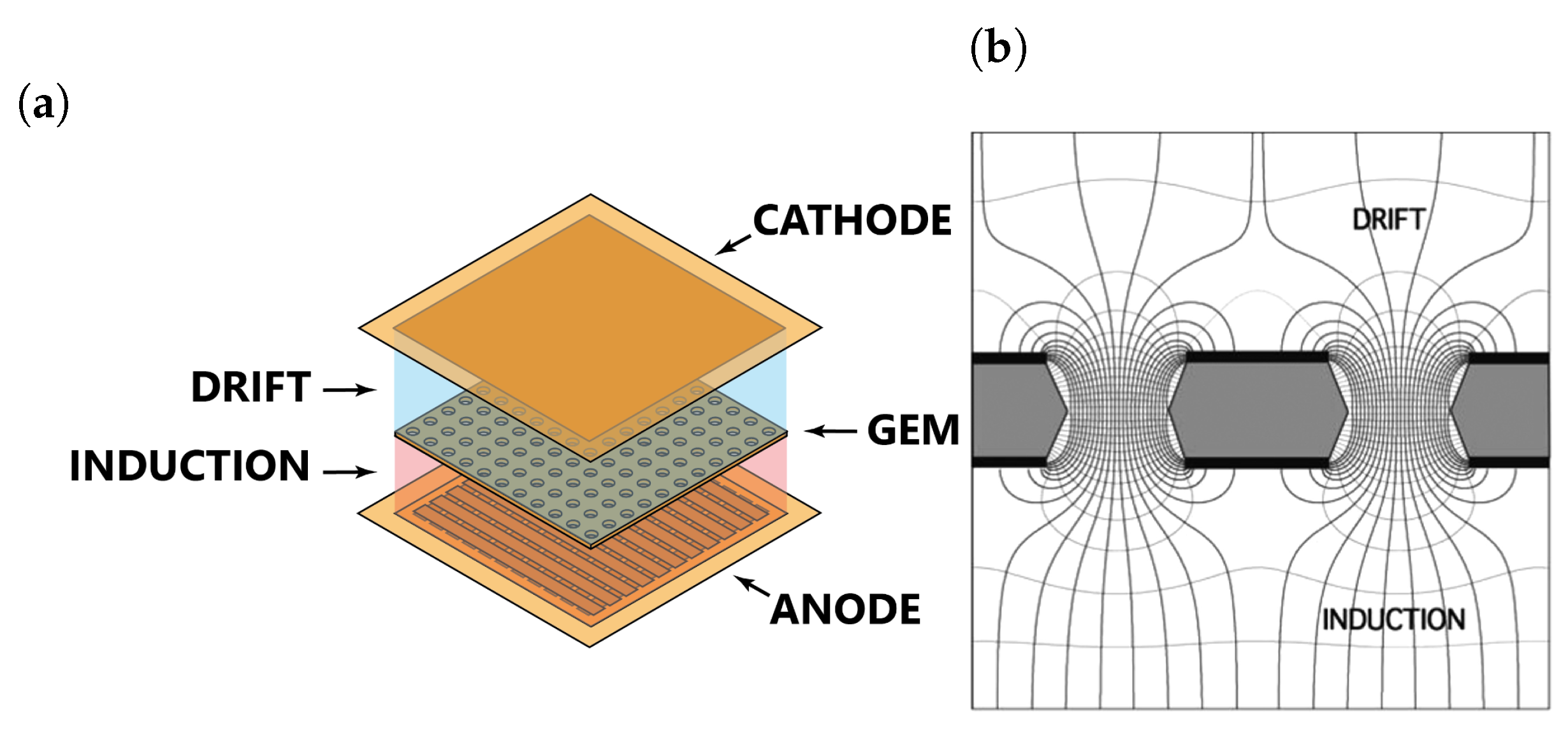
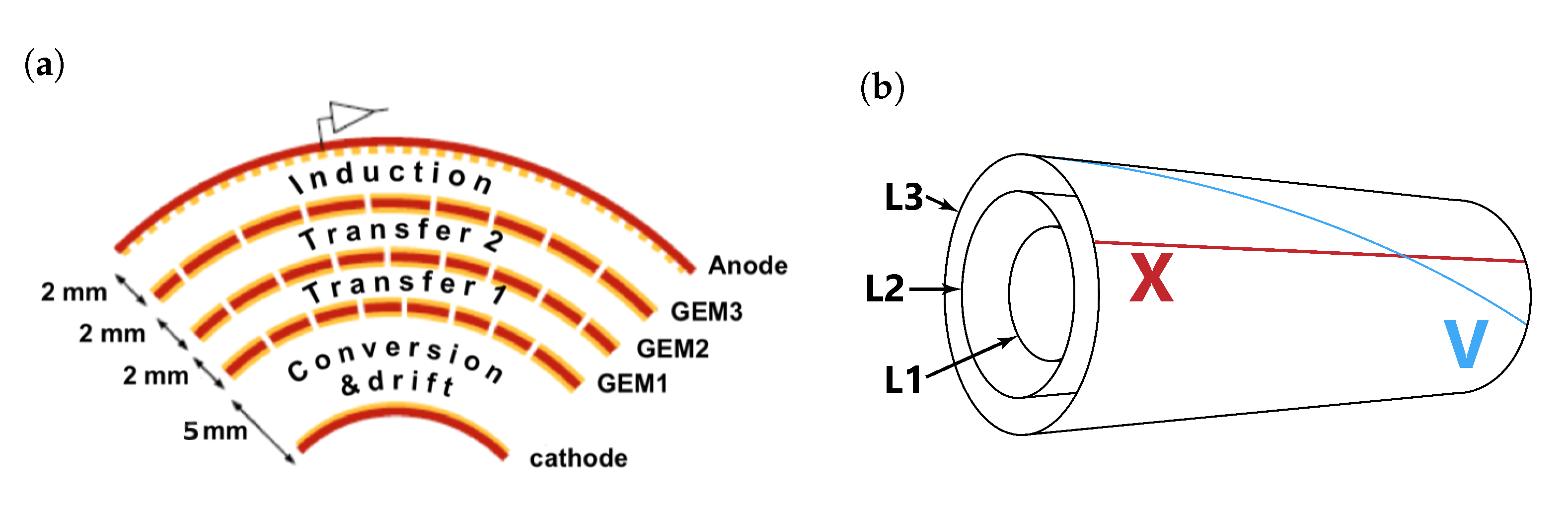
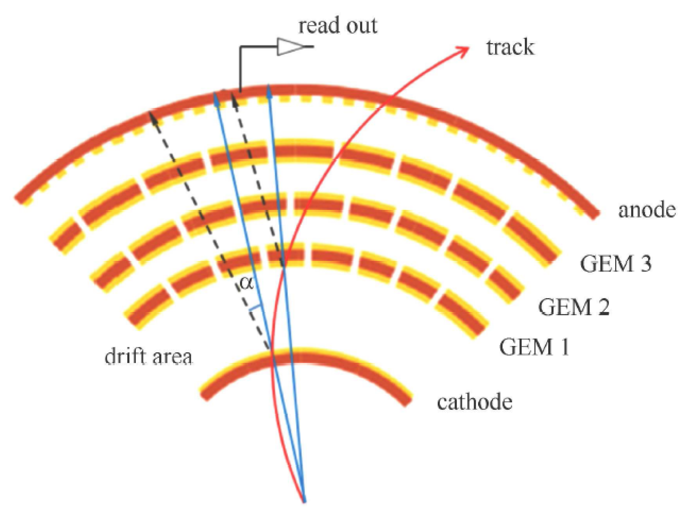
2.1. A GEM-Based Detector

A GEM is a Kapton (polyimide film with exceptional temperature resistance capable of providing good insulation) foil, copper-clad on both faces, with a high density of holes. It provides electron multiplication by means of an intense electric field of some tens of kV/cm in the holes, which is generated by applying a high voltage difference between the two copper layers. Its thickness is usually 50 µm with 5 µm copper, the bi-conical holes have 50 µm (70 µm) inner (outer) diameter, and the pitch of the holes is generally of about 140 µm.
The simplest design for a GEM-based detector is composed of a GEM foil placed between two copper electrodes that act as cathode and anode, creating a closed gas volume. A schematic representation is given in Figure 4a. Three main regions inside the detector can be identified (Figure 4b):
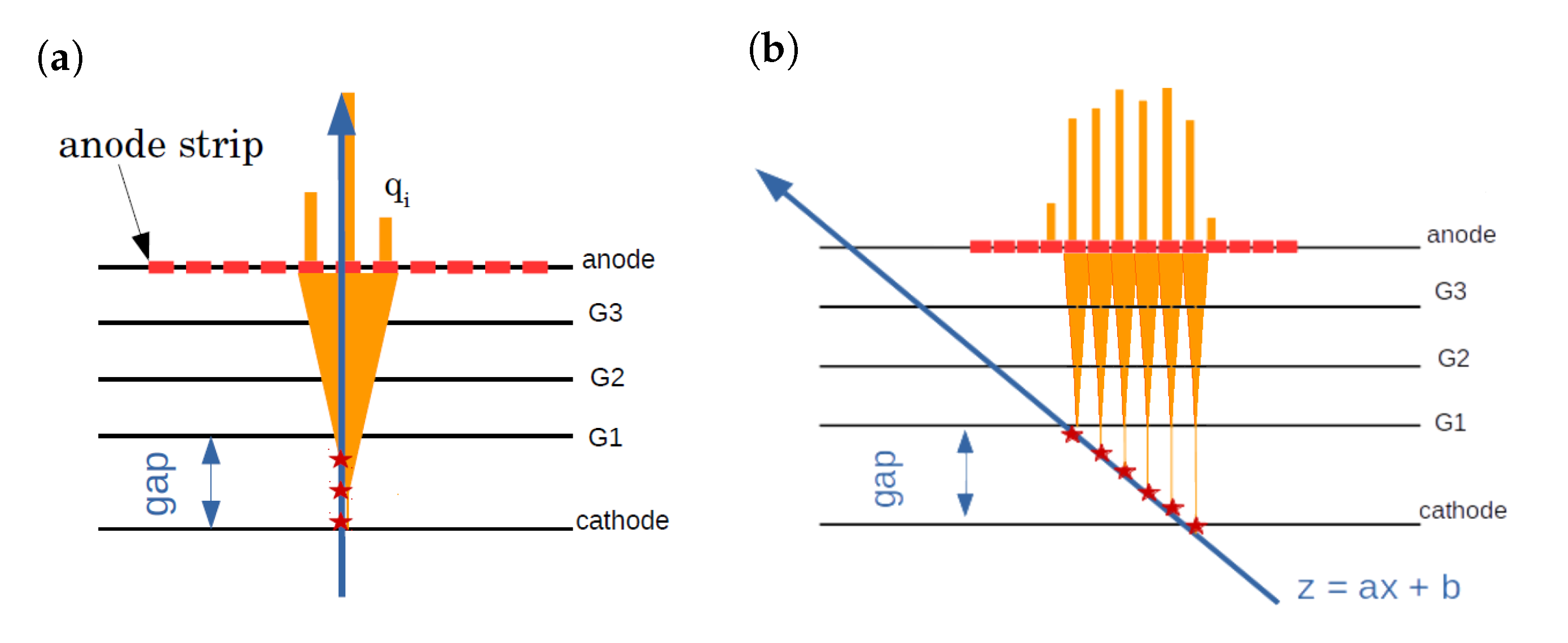
  • The drift gap, between the cathode and the GEM, is where the primary ionization takes place and, thus, the generation of electrons. Then, the electrons drift toward the GEM foil. Since the full volume is filled with gas, the ionization can also happen in other parts of the detector but such electrons will not be multiplied enough to contribute significantly to the signal;
  • The multiplication region, within the holes of the GEM foil, where the electron avalanche occurs;
  • The induction gap, between the GEM and the anode, where the electrical field drives the electron avalanche towards the anode. There, it induces a signal on a patterned readout plane.
This simple design achieves gains in the range 10 2 10 3 with lower discharge probability with respect to other gaseous detectors technologies. It is possible to increase the gain by stacking more GEM foils. Different configurations have been studied [28]. The gain values and the discharge probabilities are shown in Figure 5. The triple-GEM configuration, with a gain around 10 4 , is the most commonly used.
To further optimize the design, the gas mixture and the anode segmentation play an important role. The choice of the gas mixture is fundamental for the detection efficiency: it contributes to the ionization and to the multiplication, and it also determines the diffusion and drift velocity of the electrons. It is therefore important to choose a proper mixture that provides ionization with a high number of primary and secondary electrons (noble gases such as He or Ar) while keeping the discharge risk low. For this purpose, an organic gas is usually used as a quencher (iC 4 H 10 or CO 2 ) [29]. The anode segmentation can be done in strips or pads. Usually, 2D strips are preferred thanks to the possibility to optimize the stereo angle among them and the pitch size to maximize the charge collection and the coverage of the active area.
Triple-GEM technology has been used for 20 years and its applications are well known [27]. Many experiments such as COMPASS, LHCb, and BONUS [30,31,32] use it and its application for a tracker is almost straightforward thanks to its performance, low cost, and low material budget. Moreover, the spatial resolution, limited mainly by the geometry chosen for the anode, can reach tens of microns. The time resolution can be better than 10ns thanks to fast-moving electrons in the avalanche that quickly produce the signal [33]. Finally, such detectors can guarantee good performance even at high rate (10 8 Hz/cm 2 ) and show a good radiation tolerance, up to few C/cm 2 [34].

2.2. The Cylindrical GEM Inner Tracker

The BESIII CGEM-IT consists of three independent cylindrical triple-GEM detectors identified in the document as layers. They all share the same design and technology but each geometry is optimized to maximize the solid angle coverage (93% of 4 π ) with a material budget within the limit of 1.5 % X 0 .
For each layer, from the inner to the outer radius, it is possible to distinguish five sub-layers: the cathode, the three GEMs (GEM1, GEM2 and GEM3) and the anode. Each of them is optimized to provide an efficient operability of the detector:
  • The cathode foil has a copper thickness of 3 µm on one side of the Kapton substrate, which will face the internal part of the layer. To offer the necessary rigidity and shape, the cathode is also glued to the mechanical inner structure as will be described in detail in Section 3;
  • The GEM foils have 5 µm copper on both sides of the Kapton substrate with a specific segmentation for the two faces to optimize the High Voltage (HV) distribution, as will described later in the section;
  • The anode foil hosts the readout plane. It is segmented in 5 µm thick strips etched on both the copper sides on the Kapton foil and sealed with an additional foil of 25 µm Kapton glued on them. The strips on the two sides are oriented with different angles as shown in Figure 6b. X strips, parallel to the beam axis, provide the azimuthal coordinate and are 570 µm wide; V strips, 130 µm wide, are oriented in each layer with a different stereo angle. They give, together with the information on the X, the position in the direction parallel to the beam and reduce the ghost hit tracking. The pitch for all the strips is 650 µm. Outside the anode the cylindrical mechanical structure is also glued and, on top of it, there is an additional Kapton foil with 5 µm copper-cladding on the external side. This is the ground plane providing the reference for the front-end electronics.
In addition, two cathode-like foils are placed inside the inner and outside the outer layers to act as a Faraday cage to shield the CGEM-IT from electromagnetic interference and reduce the pick-up noise.
The mechanical rigidity of each layer is ensured by the structure glued in the inner and outer parts and by the support rings at the ends. These also guarantee the gas sealing and that the gaps between the sub-layers are the desired ones. As shown in Figure 6a, the drift gap is 5 mm, while the gaps between the GEMs (transfer gaps) and induction gap are 2 mm. At the extremities, the on-detector electronics is hosted on the outermost support ring while the HV boards are placed on additional service flanges. Table 1 illustrates the main mechanical features of the layers: inner diameter, active area length, and strip stereo angle.
The HV distribution of each layer is divided in seven separate electrodes referred to the ground plane. The cathode and the copper faces of the GEMs are directly connected to the CAEN SY4527LC mainframe with CAEN A1515CG boards, Radiall-REDEL converter and distribution patch panels. Each GEM copper plane facing the anode is divided in the so-called macrosectors. The other copper part is segmented into 10 microsectors for each macrosector. The power supply has been designed in such way around the azimuthal angle to restrain the damages resulting from discharge events in terms of energy released thanks to a reduced capacitance. In a situation where only one sector is damaged, it is possible to disable it, while keeping the rest running. For the three layers, the design foresees four, eight and twelve sectors from the inner to the outer geometry.
The gas mixture chosen as a result of different simulations and experimental tests is Ar:iC 4 H 10 with (90:10) proportions. For this configuration, the operating values of the CGEM are as follows. The electric fields in the drift, the two transfer and the induction gaps have intensities equal to (1.5/3/3/5) kV/cm; the GEM voltage difference are (280/280/275) V, from GEM1 to GEM3, corresponding to a gain of the order of 10 4 with a discharge probability below 10 6 .
An analogue readout, providing time and charge measurements of the signals coming from the CGEM-IT, has been chosen since it allows for a larger strip pitch and thus a smaller number of electronics channels. For this purpose, a dedicated Application Specific Integrated Circuit (ASIC) was designed together with its full readout chain. The charge and time information provided enables position reconstruction algorithms to achieve the required spatial resolution. Both readout electronics and software reconstruction algorithms are discussed in detail in the next sections of this review.
This design, with the presented characteristics in this review, satisfies the BESIII requirements for the CGEM-IT detector listed in Table 2.

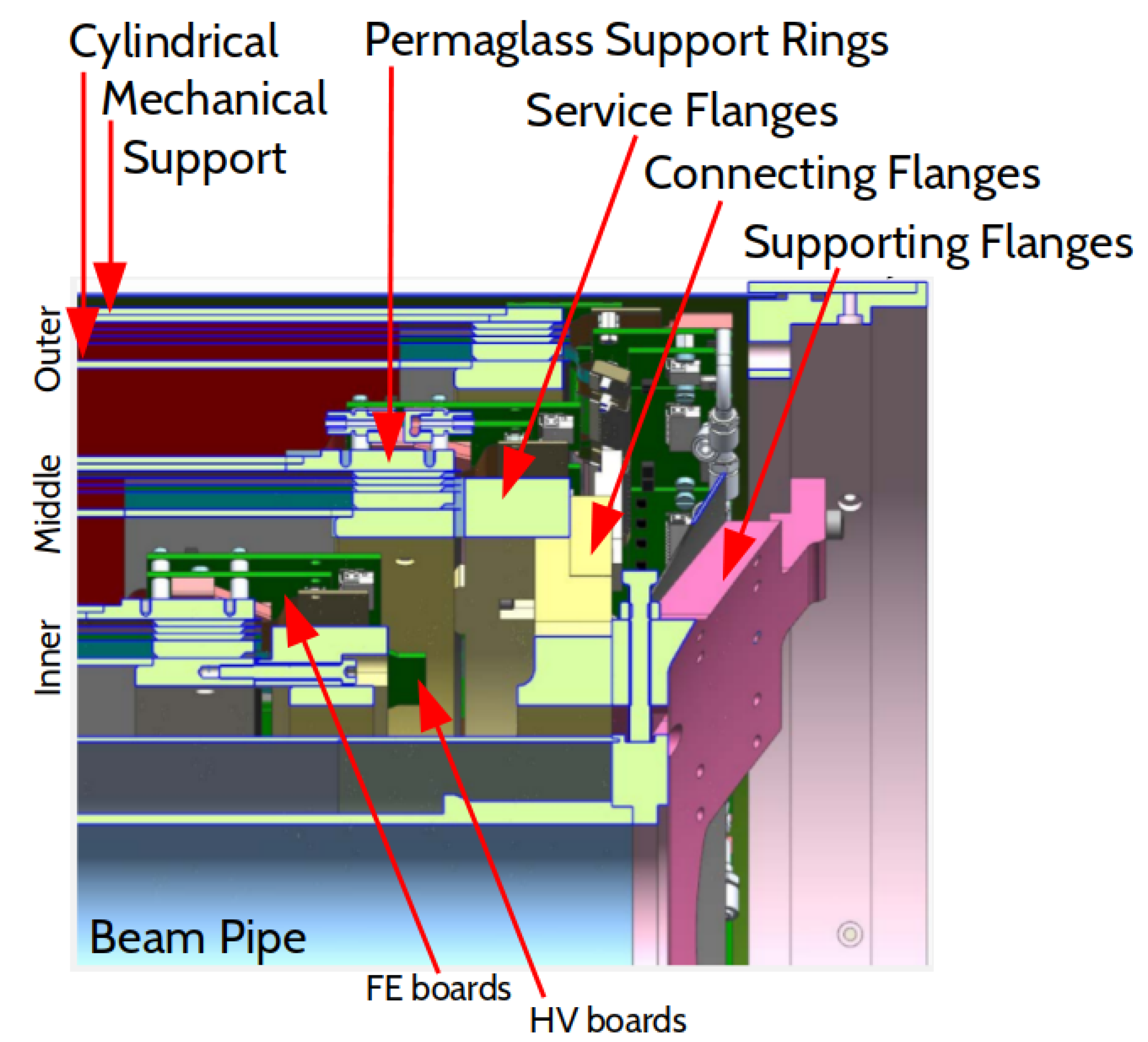
3. CGEM-IT Mechanics

This section focuses on the detector design: the choices, the development, and the tests that were brought to the final construction are discussed.

3.1. Mechanical Requirements

As indicated earlier, the CGEM-IT is a detector foreseen to be installed in an already existing experiment as a replacement for the present inner tracker. This situation implies a series of requirements to be satisfied:
  • The space available to fit at best the volume left over from the IDC;
  • The material budget to minimize the multiple scattering;
  • The performance improvement with respect to the present inner tracker.
As summarized in Table 1 and described in the previous section, the inner layer is the smallest in both radius and length while the outer is the largest. Figure 7 shows a detail of one of the ends of the CGEM-IT. It is possible to distinguish the support rings to which the different sub-layers are glued, the service flanges to host the HV boards, the connecting and supporting flanges that will be use to connect one CGEM layer to the others, and this inner tracker to the ODC in the experiment, respectively.
The cathode, the GEMs, and the anode foils are manufactured at the CERN EST-DEM workshop (Design and Manufacture of Electronic Modules Group of the Engineering Support and Technology Division). The preparation is based on the photolithographic and etching processes [37].
The support rings are in Permaglass, a fiber-glass reinforced epoxy resin, which guarantees the necessary robustness and the gas sealing. The mechanical structure has undergone major reviews to deal with the stress that the CGEM-IT will encounter in its lifetime. Since it is constructed in Italy, it needs to be shipped to China and it will be installed in the experiment. In the first production of the three layers, the mechanical structure was prepared with ROHACELL®, a light polymethacrylimide based structural foam, and Kapton sandwiches [35] but for the final detectors the choice was laminated carbon fiber foils on an Honeycomb strcture. Honeycomb is a lightweight core material based on an hexagonal cell geometry and this specific one was made by aramid fibers held together by a resin [38]. The process that brought to this decision is described in Section 3.3.

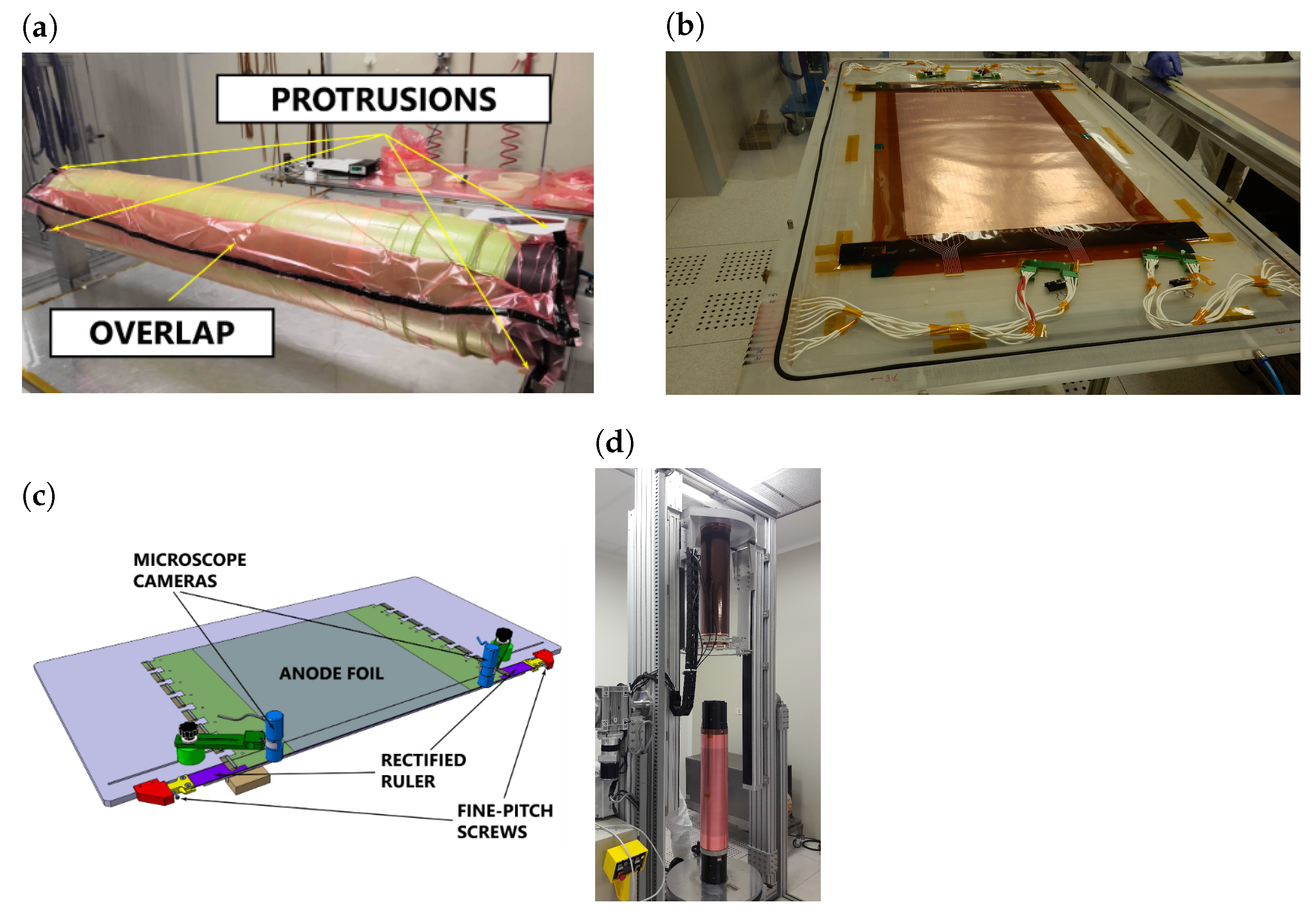
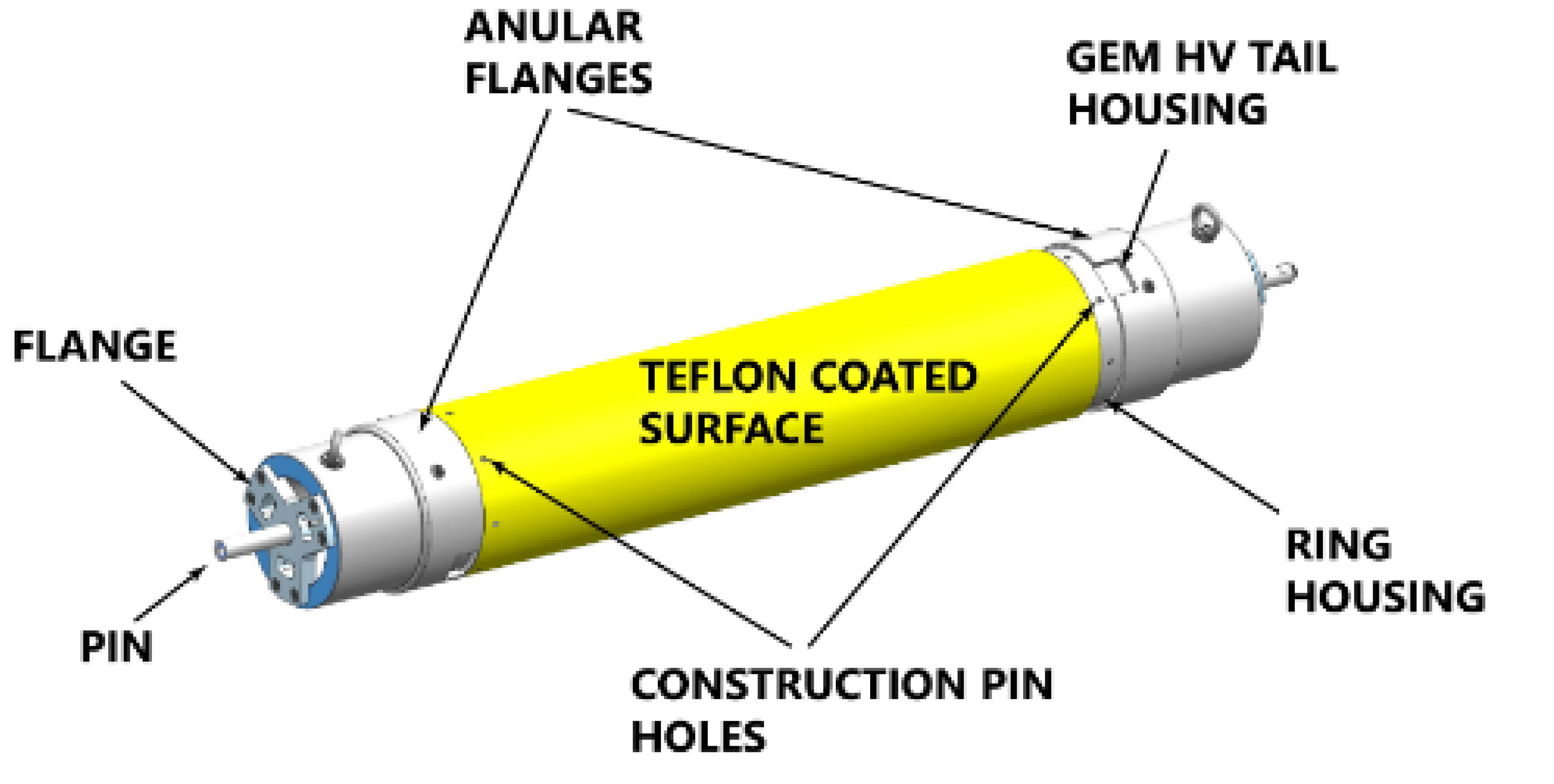
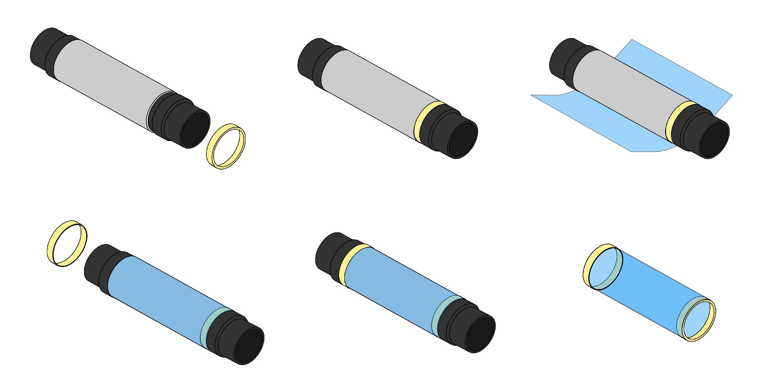
3.2. Layer Construction

The construction of two out of the three layers has been performed in Italy at the Laboratori Nazionali di Frascati, Rome, inside a class 1000 clean rooms. Each sub-layer is built separately and then assembled. Once completed, the layer is first tested in Italy and then shipped to Beijing. The construction technique is shared for all the sub-layers [26]. The cylindrical shape is guaranteed by means of rectified mandrels for gluing the foils to the support rings. A vacuum system for the curing of the glue is used.

3.2.1. Validation of the Components

Before starting the actual construction, tests are needed on every single part of the instrumentation and the construction material. Foils, mandrels, and rings are first checked to ensure that their dimensions are within the requested tolerance of 100 µm. A small deformation on any of these elements can be the source of a bigger defect in the construction or in the operation of the detector and therefore would require a second production or some correctional operations.
A test of the vacuum system is also performed. During the construction, a vacuum bag is placed around the foil and the rings on the mandrel to give a homogeneous depressurization to help the pose of the glue. For each mold, the validation is performed using a dry-run to check the compliance with the requirements and the uniformity of the system without the final elements in place (Figure 8a).
In addition, each GEM foil undergoes several tests to control its functionality. Once the foils reach the construction site, they are visually inspected for major faults as bumps or scratches. The next step is to place them, one by one, in a custom box for HV testing in nitrogen gas (Figure 8b). Here, the foil is placed and connected to a power supply to perform a first power-on. The HV is slowly raised up to 600V; if there are no discharges in 20min, the GEM foil is considered electrically ready.
Sometimes, a resizing operation is necessary to remove the excess of polymer on the foils, residual of the production. This is usually done for the anode, but sometimes it is needed for GEM foils as well. A custom machine has been developed to perform such operation with a cut precision of the order of 100 µm (Figure 8c). It consists of an adjustable rectified guide ruler, two microscope cameras, and a sled to hold the scalpel blade. Once the foil has been set on the table and all the alignments have been checked, the blade is sled in a single movement along its length. The more precise the cut is, the easier the operation of gluing is.
A Vertical Insertion Machine (VIM) has been constructed to assemble the five sub-layers (Figure 8d) [39]. As it will be described in the following paragraph, it allows the insertion of each sub-layer into the other and also the gluing of the rings at both ends thanks to the possibility to rotate the system by 180°. This handling of the sub-layers is very delicate and therefore an alignment of the full machine is requested before starting to ensure the 100 µm precision for the insertion.
Once all the components necessary for the construction have been validated, the preparation of each sub-layer can begin.

3.2.2. Preparation of the Sub-Layers

The technique used for the preparation of a cylindrical layer has been optimized for all the sub-layers to be almost the same. The main difference concerns the cathode and the anode, which are glued with the mechanical structure and require more working steps. Depending on the dimensions of the layer, the cylindrical sub-layers consist of either one or two foils. In the inner layer, all the sub-layers are made of single foils. In the others, they are built with two separated foils which are glued together to create a larger foil. Each piece is prepared on planar surfaces and, as will be described later in this section, is shaped in the desired cylinder. This mechanism produces dead zones at the junctions of the foils, called overlaps, of a few millimeters thick. These are aligned in the final assembly to minimize the loss of the active area.
Each sub-layer has its own mandrel. Figure 9 shows an example. It is built of anodized aluminum, with Teflon coated in the middle part of its surface. Such a structure grants an easy release of the sub-layer during the next assembly steps without any residual glue or aluminum dust. In addition, the mandrel is constructed with the possibility to be rotated around its axis to help the construction process.
The procedure, sketched in steps in Figure 10 [26], starts by placing on the ring housing the so-called inner-ring, to which the foil will be glued. A preliminary dry-run of the movement of the foils around the mold is performed without glue. If this procedure is successful, the glue, Araldite 2011 (bi-component epoxy adhesive, used when the surface of glue exposed to the gas is minimal to minimize out-gassing effects), is placed on the inner-ring and on a 2mm wide strip along the foil length for the overlap. Now the foil is wrapped around the mold and glued.
For the sealing, a vacuum bag is placed around the entire system, sealed and left to rest for at least 10 h. The final step is to place the so-called outer-ring at the extremity opposite to the inner-ring and glue it on the foil. A narrow opening on the ring guarantees its placement in the desired position at the end of the foil and a better seal during the gluing process. Additional time with the vacuum bag is therefore required. The very last step is to seal the outer-ring cut with Araldite 103, a bi-component epoxy adhesive which can be exposed to the gas.
For the cathode and the anode, the procedure is basically the same with the addition of a few more steps. For the cathode, the first thing to be wrapped on the mold is the mechanical structure built with foils of Kapton, carbon fiber, and Honeycomb. On top of this support, it is possible to glue the cathode foil. The other cylindrical mechanical structure, built with the same sandwich of the cathode, is placed between the anode and the ground plane. Since the anode hosts the readout strips, the cylindrical gluing of the two foils can not be done by overlapping, but an additional Kapton band is used to hold the foils together.
At this point, all the sub-layers are ready to be assembled together.

3.2.3. Layer Assembly
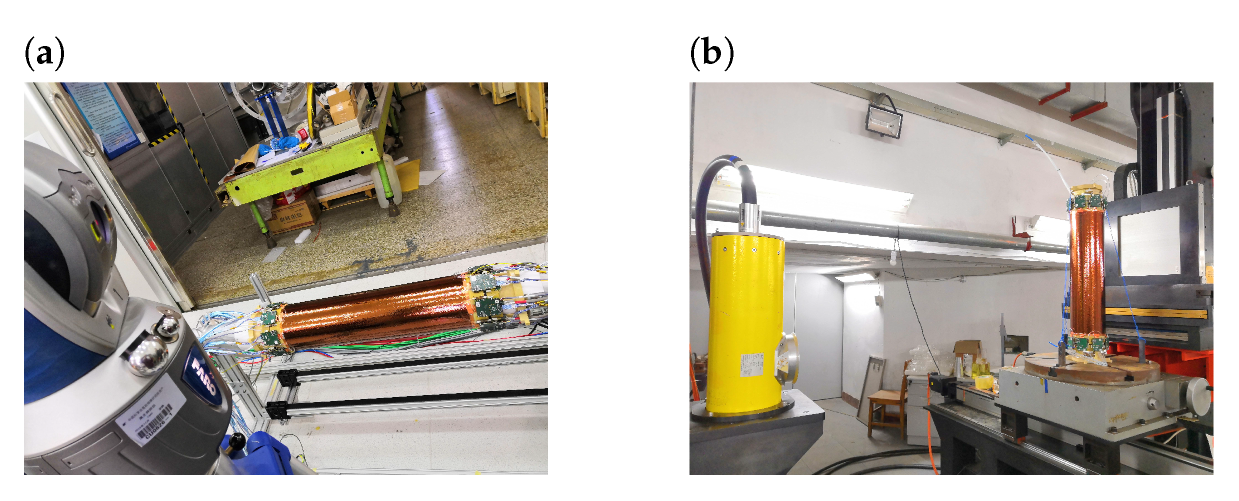
The layer is assembled using the VIM, a numerical control machine developed specifically for these operations (Figure 8d). Its tasks are the handling and the precise positioning of the mandrels and, therefore, of the cylindrical sub-layers.
This construction starts with the outer layer, the anode, and ends with the cathode insertion and the final sealing. The anode on its mandrel is placed in a vertical position inside the machine that holds it by the ring on top. This allows lifting the anode sub-layer and separating it from its mandrel which, at the end of this operation, is removed from the machine to leave the space for the following sub-layer. The anode is then lowered around the second sub-layer until they are properly aligned. To glue the two sub-layers together, a suitable mixture of Araldite 103 and silica micro-spheres is used to penetrate predictably in the space between the rings. After 22 h, the VIM is rotated by 180 to allow the gluing on the other end of the cylinder.
This procedure is repeated for all the remaining mandrels. At each step the layer is visually checked to ensure that there are no major defects on the visible surface. Once the assembly of the five sub-layers is complete they are still inside the insertion machine, and the final sealing and the placing of the gas connectors are performed using Araldite 2011. Now the layer is solid and it can be manually slid by hand onto the horizontal support to mount the service flanges and the connectors of the HV electrodes, through their tails that, by construction, pass through the rings at the extremities.
The CGEM-IT layers are assembled together in Beijing, for the final commissioning. This is done by means of a custom machine with a cradle and sleights to slide one layer on top of the other and secure them together [36].

3.3. Investigation

A Quality Assurance and Quality Control (QA/QC) protocol has been developed for each layer to reassess the proper functioning after major operations such as construction or shipment. This protocol includes gas checks, resistance and capacitance measurements of the HV channels, and a power-on procedure.
A first production of the full CGEM-IT was completed, tested, and shipped to Beijing. There, the validation after shipment pointed out issues on the inner and the outer layers. Therefore, a thorough investigation started to understand the nature and the entity of these problems [38].
The first tests performed were the less invasive ones: another resistance and capacitance measurement for each HV sector and a measurement of the external surfaces with a laser. The former is performed with a multimeter through the HV connectors of the layer. Microsectors and macrosectors of the same foil as well as the ones of facing foils were checked to measure the homogeneity of the gaps and to establish if any shortcut occurred. If shortcuts are present, the resistance is finite; if there is any deformation in the gap, the value of the capacitance changes compared to the neighboring ones. This gave a mapping of the electrical status of the layer: some values differed from the expected ones and eventually it was possible to decide to unplug the respective microsectors. The laser measurements, on the other end, were useful to check external deviation from the nominal shape caused by possible improper handling such as torsion, stretch, or compression. They were performed by means of a laser tracker measuring multiple times the circumferences along the full length of the detector (Figure 11a). In our case, all the layers successfully passed this check, showing no major deformations. A measurement like this is extremely useful, even if it depends heavily on the precision of the instrument: the defects must be of the order of magnitude of 1mm otherwise they cannot be spotted.
A second useful test was added to this investigation: the computed tomography (CT) scan. It was performed by means of a scan available at IHEP. At the beginning, X-ray scans were performed to adjust the beam intensity to the composition of our detector. Afterwards, with the detector in a vertical position, as shown in Figure 11b, slices orthogonal to the axis of the cylinder at different lengths have been scanned. It was possible to distinguish, from the inside, the cathode with the mechanical structure, the three GEMs, the anode with the other mechanical structure and the external ground plane. The results are dominated by the resolution of the device, but it is still possible to distinguish every component. In some part of the detector the foils were found distorted. This qualitative analysis confirmed the resistance and capacitance mapping and allowed the quantification of the damages.
The last part of this investigation was the most invasive and was performed only on the layer that was declared to not be working—the outer one. This part consisted of the mechanical opening performed foil by foil, from the outer sub-layer. After the removal of each foil, a visual check of the defects pointed out by the previous measurements has been performed. Moreover, a study of their correlation with the mechanical structure was performed by means of stress tests such as pushing or pulling the rings or similar unconventional movements.
This full investigation brought to light a partial fragility of the selected Rohacell–Kapton sandwich related to the excess of vibration or in case of unexpected events that can occur in a travel from Italy to China. It was therefore decided to improve the mechanical robustness, knowing that the radiation length of the detector increases. The final choice is to use laminated carbon fiber foils on a honeycomb structure that still keeps the material budget within the limits. All the performed tests taught us a list of possible options to analyze a detector, such as the CGEM one, whose interior components are no longer accessible once it has been completely sealed.

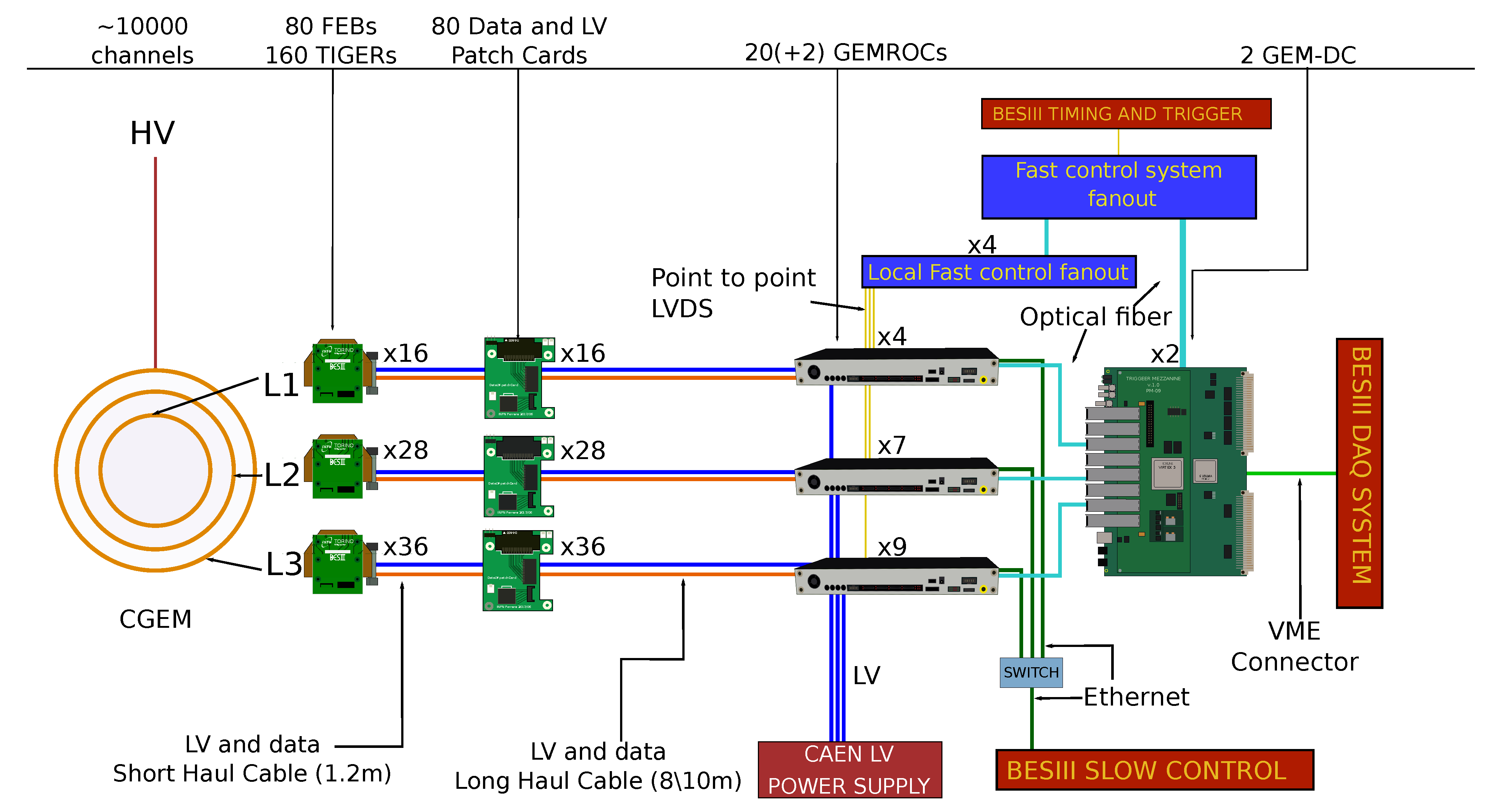
4. CGEM-IT Electronics

This section describes the CGEM-IT readout electronics, discussing the main features of each block composing the full chain, including the front-end ASIC and the off-detector modules, based on Field Programmable Gate Array (FPGA) devices, for data selection, and storage. An overview of the CGEM-IT electronics readout chain is displayed in Figure 12 and it can be divided into two main blocks: the on-detector and the off-detector electronics.
The on-detector electronics comprises 160 Torino Integrated Gem Electronics for Readout (TIGER) chips assembled on 80 Front-End Boards (FEB). TIGER is a mixed-signal ASIC and includes 64 parallel channels performing amplification and processing of the signals coming from the CGEM-IT, providing a fully-digital output, with charge and time information. This information is used by software reconstruction algorithms to improve the system spatial resolution compared to the one achieved with a simple binary readout. With this analogue readout, it is possible to reduce the total number of electronics channels down to ∼10,000 [40], thus resulting in a lower total power consumption and a smaller number of cables required for the front-end electronics.
Digitized data is transmitted from the chip to the off-detector electronics GEM Read-Out Cards (GEMROCs), where trigger-matching operations are performed, using the time information provided by the ASIC. This allows the system to store only the data corresponding to the BESIII trigger signals, which are of interest for the experiment. Each GEMROC module can handle up to four FEBs (eight chips, 512 electronics channels), therefore, the tracker can be read entirely with 20 GEMROC modules, but 22 will be used in the final experiment in order to provide a more symmetric readout scheme for the two sides of each CGEM-IT layer. Eighty Data and Low Voltage Patch Cards (DLVPC) connect the short haul cables coming from each TIGER FEB to the long haul cables going to the GEMROC modules. These cards allow easier cable management by disentangling the arrangement of long and short cables and can also provide a common ground reference for the system. The readout chain is completed by two GEM Data Concentrator (GEM-DC) boards, which collect data selected by the GEMROCs to build the complete events and store them in the BESIII Data Acquisition System via the Versa Module Eurocard (VME) bus.
In addition, the on-detector and off-detector electronics are supplied by a dedicated low voltage (LV) power distribution system, mounted on a CAEN SY5527LC mainframe hosting four CAEN A2519 boards to supply the GEMROC modules and three CAEN A2517 boards to provide the power supply to the TIGER ASICs through the GEMROC LV distribution section [21]. The system can be controlled remotely via Ethernet and provides power on/off capability and monitoring of the current and voltage on each channel of the boards.

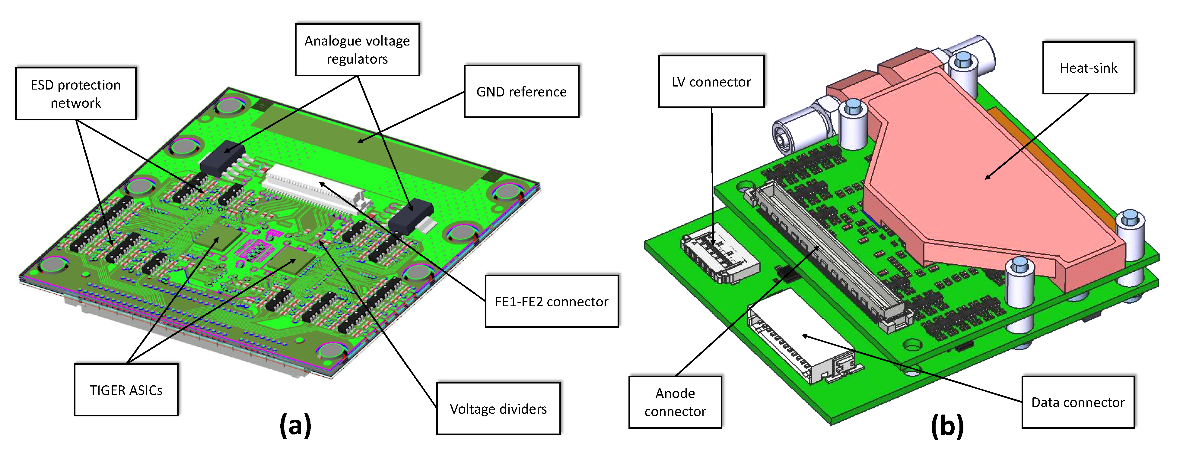
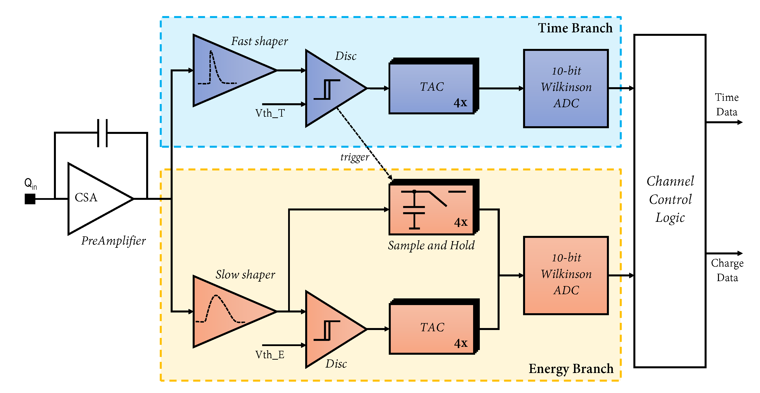
4.1. Front-End Boards
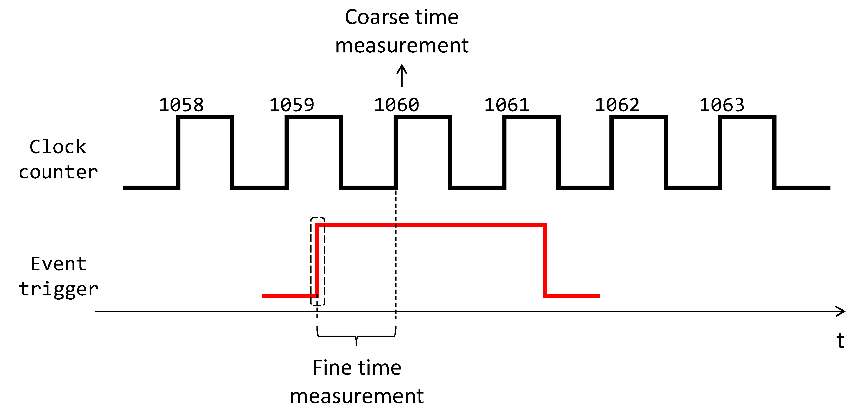
The 160 TIGER ASICs needed to fully instrument the CGEM-IT are hosted on 80 FEBs. Corresponding to the increasing size of the three coaxial layers that make up the CGEM-IT, the FEBs are distributed as follows: 16 FEBs for the inner layer, 28 FEBs for the middle layer, and 36 FEBs for the outer layer. The boards have a compact design [41] to fit into the limited space in the inner part of the BESIII spectrometer.
Each FEB, as shown in Figure 13, mounts two TIGER chips and is made of a stack of two printed circuit boards (PCB): FE1 and FE2. The analogue-most PCB (FE1) accommodates the two ASICs as well as power regulators and surface-mount device voltage divider circuits for proper chips biasing, while the digital-domain PCB (FE2) mounts the low-voltage differential signaling (LVDS) buffers and the connectors to interface the FEBs to the off-detector electronics for data transmission and power supply [42]. On FE1, a Hirose FX10A-144P-SV connector provides the interface towards the detector anode: for each channel input, an electrostatic discharge network provides protection against the detector discharges. A liquid cooling heat exchanger plate, mounted on the external side of FE1, cools down the electronics to operate the ASICs at stable temperature and limit the heat dissipation towards the other BESIII sub-systems surrounding the CGEM-IT.

4.2. Tiger ASIC

TIGER is a 64-channel mixed-signal ASIC developed for the readout of the CGEM-IT [43]. The chip has been designed and fabricated in a cost-effective 110 nm complementary metal-oxide semiconductor (CMOS) technology, occupies an area of 5 × 5 mm 2 and operates with 1.2 V and 2.5 V power supplies. The analogue front-end of TIGER, designed to cope with the requirements of the CGEM-IT, is optimized for input signals in the 2–50 fC range and aims to achieve a noise below 2000 electrons r.m.s. for an input capacitance up to 100 pF and a maximum power consumption of about 12 mW/channel.
The block diagram of one TIGER channel is displayed in Figure 14. The very front-end of TIGER features a charge sensitive amplifier (CSA), based on the architecture described in [44,45], which senses and amplifies the small detector current signals. The CSA gain, defined by its feedback capacitance, is set to 6.67 mV/fC while a transconductance feedback implemented with current mirrors provides, in a very limited area, an equivalent resistance up to tens of M Ω , thus establishing the DC feedback current needed to properly bias the input stage [46]. The same network is also used to feed the output stage where the signal is split into two identical branches, providing pole-zero cancellation and additional charge amplification.
The two output branches are coupled to two shapers optimized for timing and charge measurement. The time branch employs a simple CR-RC shaper with 60 ns peaking time for low-jitter time measurements, while the energy branch shaper adopts a topology with four complex conjugate poles [47] and larger shaping time (170 ns) for a better charge resolution and noise optimization. For each shaper, a baseline holding (BLH) loop, similar to the one presented in [48], suppresses any DC current coming from the input stage and sets the shaper’s output baseline to an external reference voltage, which can be set off-chip through a dedicated pad.
Each shaper output is fed to a leading-edge discriminator with hysteresis and programmable 6-bit digital-to-analogue converter (DAC) for threshold adjustment to correct offsets and mismatches among the 64 channels. The two discriminators in each channel allow a dual-threshold readout mode where the time branch can be set to a very low threshold for optimal timing performance, while the better signal-to-noise ratio of the energy branch is used to discard events induced by noise. This implies that the ASIC is self-triggered and can produce output data without any external trigger: each signal above a given threshold configuration is taken as a good event and digitized by the versatile channel back-end, which runs at a 166.6 MHz clock frequency and allows for simultaneous measurement of input signals time of arrival and collected charge.
The time measurement concept is shown in Figure 15 and is evaluated with two levels of accuracy. The coarse time information comes directly from the chip master clock, thus resulting in a time binning of about 6 ns. The fine time information is extracted and digitized by low-power Time-to-Digital Converters (TDC) based on analogue interpolation to achieve a sub-clock resolution. The same architecture is described in [49,50]. On each channel, a set of four Time-to-Amplitude Converters (TACs) is employed to convert the time between the hit triggered by the discriminator and the next clock rising edge into a defined voltage level. The TAC analogue voltage is then digitized by a 10-bit Wilkinson Analogue-to-Digital Converter (ADC), common to the four TAC buffers. The combination of the coarse and fine time measurements provides a fully reconstructed event timestamp. With an interpolation factor of 128 and a 166.6 MHz clock frequency, this leads to an overall TDC time binning below 50 ps, thus making the TDC quantization error negligible and the time resolution limited only by the sensor and the front-end amplifier performance.
In addition, an array of four Sample-and-Hold (S&H) circuits is deployed in the energy branch. These blocks are controlled by the channel digital logic and employed to sample the slow shaper output and capture its peak voltage, from which the input signal charge can be extracted. This sampled voltage is digitized by the Wilkinson ADC shared with the TDC of the energy branch. As a backup solution, the charge information can be also extracted from the pulse duration measured with the Time-over-Threshold (ToT) technique. Figure 16 shows an example of the chip response to different input charge signals for the two operation modes: S&H mode and ToT mode. The response of the S&H is linear, but saturates after 45–50 fC, while the ToT readout allows the system to extend the input dynamic range beyond the saturation point of the front-end amplifier or the ADC, but its response is not linear and depends also on the threshold setting.
One of the major drawbacks of the Wilkinson ADC technique is the large conversion time, which can take up to 8 µs. This issue is mitigated by having a multiplicity of four for the TAC and S&H capacitors. This solution de-randomizes the events arrival time distribution, thus achieving an event rate of 100 kHz per channel with an efficiency better than 99%.
Digitized data is transmitted off-chip through a set of four LVDS links, working at 2.5 V. The 64-bit event words are transmitted over one of the serial links in Single Data Rate (SDR) or Double Data Rate (DDR) mode, with 8b/10b encoding. In BESIII, only two LVDS links are used in SDR mode to reduce the chip power consumption as well as the size of connectors and cables needed to interface the FEBs with the GEMROC modules. SDR operation at 166.6 MHz clock frequency implies a total output bandwidth of 333 Mbit/s. This allows each chip to transmit 4.1 × 10 6 events/s, thus implying a maximum event rate of about 60 kHz/channel, which is still above the requirements for BESIII. The ASIC is configured through a 10 MHz Serial Peripheral Interface (SPI) performing read and write operations of the on-chip configuration registers, made of a 169-bit global configuration vector and a 125-bit per channel configuration vector.
The ASIC digital back-end and control logic, which manages the TDC and S&H operations, are inherited from another family of ASICs developed for medical applications [51,52]. Due to the BESIII radiation environment in which TIGER is expected to operate, the digital logic has been protected against single-event upset effects by using triple modular redundancy for finite-state machines and Hamming encoding for configuration payload. Inside BESIII, the CGEM-IT inner layer is expected to cope with a Total Ionizing Dose (TID) of 10 krad per year. The on-detector electronics will have to withstand the same radiation environment: the adopted 110 nm process technology has already been tested up to TID of 5 Mrad, which is much higher than the total dose delivered during the years of BESIII operation, and the results showed very low degradation effects [53]. In addition, some samples of the PCB that host the TIGER chips have been irradiated to about 30 krad in order to evaluate the radiation damage on voltage regulators and other passive components mounted on it and the measured 0.7 ÷ 0.8% variation on voltage outputs is fully acceptable for this application.
After a first prototype version, from which some design issues were detected and corrected [54,55], the final version of TIGER was produced in a dedicated engineering run for the full instrumentation of the CGEM-IT. The on-silicon electrical characterization proved the full functionality of the ASIC: all measured parameters showed good agreement with the design specifications and expected performance. The front-end provides a linear response for input signals up to 50 fC, with a total gain of about 12 mV/fC. The measured equivalent noise charge (ENC) is less than 2000 electrons for both time and energy branches and an input capacitance of 100 pF, while keeping the power consumption below 12 mW per channel. The low-noise front-end, coupled with the very good TDC performance, also results in an overall time resolution below 5 ns. The relevant chip specifications are summarized in Table 3. More details about the ASIC architecture design and the electrical characterization results can be found in [23].
In order to fully instrument the CGEM-IT, more than 160 chips have been tested, validated, and calibrated through an automated procedure, developed appositely for this application, which generates look-up tables to convert the ASIC digital output to known physical quantities, i.e., input signal charge and time of arrival.

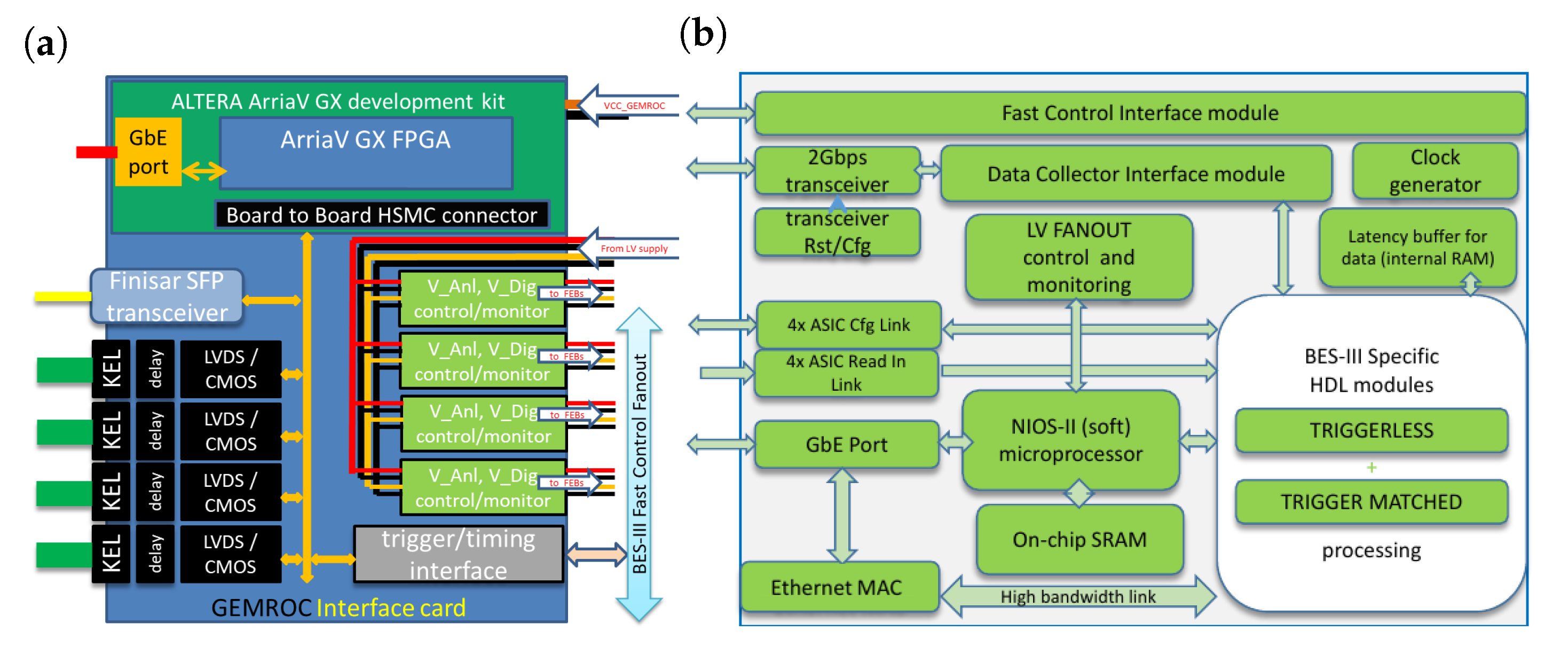
4.3. Off-Detector Electronics

The GEMROC modules and the GEM-DC boards are the two main blocks composing the CGEM-IT off-detector electronics. More details about these modules and the DAQ system can be found in [21].
The GEMROC modules manage the configuration and readout of the TIGER ASICs. They mount an ALTERA Arria V GX FPGA [56], coupled to a custom Interface Card through an High-Speed Mezzanine Card. The Interface Card handles the electrical and physical interconnections towards the FEBs, the GEM-DC, and the BESIII Fast Control system, the unit which distributes to all BESIII sub-systems the signals used for timing synchronization and event triggering.
The GEMROC receives a 41.65 MHz clock signal from the BESIII Fast Control system and processes it with its internal phase-locked loop (PLL) circuits to deliver to the front-end electronics the required 166.6 MHz clock signal. The GEMROC is also able to generate itself the clock signal for standalone operations: in this configuration, one GEMROC acts as the master module and generates and distributes the clock to the other GEMROC modules. The BESIII level 1 trigger is a hardware trigger generated by a set of BESIII sub-systems and allows the selection of good physics events with high efficiency: it reduces the backgrounds related to cosmic rays (2 kHz) and beam (20 MHz) to a level smaller than the 2 kHz physics event rate, thus resulting in a maximum trigger rate of 4 kHz [57]. It has a 1.6 µs acceptance window and a 8.6 µs latency. This trigger is sent by the BESIII Fast Control system to the GEMROC modules and used to flag, among the raw data coming from TIGER chips, the one to be saved.
A block diagram of the hardware deployed on the GEMROC Interface Card is displayed in Figure 17a. Four KEL-8822 connectors, interfaced with LVDS/CMOS buffers, allow for the communication with the FEBs, while the optical fiber interface between the GEMROC and the GEM-DC is provided by a Finisar SFP transceiver. The Interface Card also mounts a connector to distribute the clock, trigger, and control signals between several GEMROC modules. The main features of the GEMROC FPGA firmware are shown in Figure 17b and include:
  • Clock generation, synchronization, and distribution to the front-end electronics;
  • LV fanout control and monitoring of TIGER bias voltages, drained currents, and operating temperatures;
  • Read and write operations of TIGER configuration registers;
  • Readout of TIGER raw data, with trigger-less and trigger-matched data processing;
  • Communication with the DAQ computer or BESIII slow control system through a Gigabit Ethernet (GbE) port;
  • Data collector interface to build packets to be sent through GbE with a User Datagram Protocol (UDP) or optical connection.
The GEMROC firmware allows for two different readout modes, trigger-less and trigger-matched. In trigger-less mode, all data incoming from the TIGER chips are collected and transmitted to the computer running the acquisition via the GbE port using the UDP protocol. The GEMROCs directly communicate with the DAQ computer and do not perform any data selection. This mode is for standalone operation used for debug and calibration purposes to study the optimal TIGER configuration parameters (e.g., threshold equalization). Trigger-matched mode is used during physics acquisition runs, i.e., when the high number of channels to be read does not allow for a trigger-less operation without saturating the GbE throughput. In this mode, raw data from TIGER chips are stored in a circular buffer waiting for the BESIII level 1 trigger. When it is received, trigger-matched operations are performed, selecting data from the buffer which includes the correct trigger time window. For each trigger signal, a formatted packet is then created, enclosed by header and trailer event identification words. These packets can be transmitted via optical fiber link to the GEM-DC modules, but can also be sent, as a UDP packet, directly to a computer running the acquisition over the GbE port. This second mode is suitable when operating the CGEM-IT setup in standalone, thus bypassing the BESIII DAQ system.
The GEM-DC boards collect trigger-matched data packets transmitted by all GEMROC modules and merge them together to produce the final CGEM-IT events. These events are time sorted and framed to match the data format of the BESIII DAQ system, to which they are finally transmitted through the VME interface. The hardware design and many firmware functionalities of the GEM-DC boards are inherited from the Read-Out Driver modules developed for the KLOE-2 inner tracker [58] and other previous applications [59].
A Graphical User Front-end Interface (GUFI, Ref. [21]) software which provides the tools to configure both GEMROC modules and TIGER chips and then run the acquisition has been developed. This software is written in Python and includes tools to monitor the readout chain and DAQ status and test and configure the TIGER chips. The delays for the LVDS links alignment can be automatically optimized for bug-free data transmission. A threshold optimization algorithm performs 2D threshold scans on each channel and sets each threshold to a user specified value that matches the desired noise rate. This software has been successfully used during the integration test campaign for the validation of the readout chain up to the GEMROC modules. In these tests, GEM-DC were not employed yet, so the GEMROCs were directly read by the PC running the acquisition through the GbE port. Functionalities also needed in the final experiment are currently being integrated into the BESIII DAQ system control utility.

5. CGEM-IT Software

This section gives an overview of the software for Monte Carlo (MC) simulation and reconstruction of the CGEM-IT, within the general software framework of the experiment.

5.1. General Software Framework

BESIII offline software tools are organized in the framework called BESIII Offline Software System (BOSS) [60]. In order to accommodate the CGEM-IT specific code, a customization of the BOSS framework, called CgemBOSS, was created. In this framework, the drift chamber package was modified in order to delete the geometric description of the IDC and remove all its contributions to the reconstruction, to make room for the CGEM-IT in both simulation and reconstruction. Beside this, the structure of the framework is identical in both BOSS and CgemBOSS.
The framework is written in C++ language and Object-Oriented. It is based on the GAUDI architecture [61] and linked to external high energy physics libraries, as CERNLIB [62], CLHEP [63], ROOT [64], and Geant4 [65]. The software configuration management is performed through the tool CMT [66] and the revision control by CVS [67]. MYSQL [68] is used as the database server. The primary operating system for which the framework was optimized is the Scientific Linux CERN, but recently it has been replaced by the CentOS distribution.
The MC simulation tool has been inherited from the previous steps of the development of the experiment and consists of a set of event generators, the particle transportation through the detector, based on Geant4, and the simulation of the detector response, i.e., the digitization. The MC event generator provides the events in the data format HepEvt, the simulation provides detector hits and finally the digitization provides the Raw Data, containing the MC truth. The complete set of MC tools is called BESIII Object-Oriented Simulation Tool (BOOST) and is completely embedded in the framework.
The CgemBOSS framework is based on the GAUDI software architecture, developed originally for the LHCb experiment and has since then been adopted elsewhere. Presently, it is still very popular and it is the base structure on which Key4hep, the common software for all future accelerators (Circular Electron-Positron Collider, Future Circular Collider, International Linear Collider, Compact Linear Collider), is going to be implemented [69]. From the beginning, it has been intended to be a flexible tool, made by many components, decoupled from the rest of the software, in such a way that each of them may be implemented independently, refined at a later stage and even replaced without too much effort and without modifying the rest of the code. The modularity of the code allows the use of third party software as well as easy alignment with the latest implementations and the newer experiments.
The first pillar on which GAUDI stands is the separation of objects and methods handling them in different classes: the data and the functions, respectively. The two basic elementary function classes which can handle data objects are the algorithm classes and the service classes. The algorithms contain the methods to actually process the data and are managed by the application manager: they perform actions at each event. The service classes provide the algorithms with access to different quantities, which do not change through the run, but are shared by the whole code and are needed in different stages. Examples of services are the ones to access geometric parameters, the magnetic field value, the calibration parameters and so on. An instance to the needed service can be created inside the algorithm and used by it.
The data processing routines contained in the algorithms do not act directly on persistent data, but they operate on transient data, in order to decouple the algorithms from the objects furthermore. Three kinds of persistent events are defined in the CgemBOSS framework: raw data, reconstructed data, and Data Summary Tape (DST) data. The detector geometry is stored in the Geometry Description Markup Language (GDML) file, an application-independent persistent file format written in a specialized XML-based language. It is identical for simulation and reconstruction. The calibration, alignment, and environmental parameters are stored in a database and associated with the run numbers; they are retrieved when needed by a dedicated calibration service.
The simulation of the passage of particles in matter and the corresponding physical interactions are simulated with the Geant4 [65] package. It is one of the most used particle transport engines in high energy physics. It provides the tools to implement the geometry of the detector, set the sensitive volumes to collect energy deposition and other MC particle information, as well as the electric and magnetic fields. It can be interfaced to many particle event generators, thus granting the possibility to get the kinematics of the original event consistent with the physics under study, which depends on the energy range, the particles into play, and the specific objectives of the measurement. Also, the information at each step of the propagation is accessible to monitor the particle behavior in every material and part of the geometry. The correct physics list, which best simulates the physics in the specific energy range, must be selected and a series of cuts and threshold levels that influence the treatment of the various physics processes can be set to optimize the precision and the speed of the simulation.

5.2. Geometry Description and Simulation

The geometry of the CGEM-IT is implemented in the CgemBOSS framework, including both the active and passive volumes.
The geometric dimensions have been inserted in the geometry description as parameters and are read at run-time from an ASCII file. This was necessary in order to keep up with the final steps of the R&D to define and optimize the CGEM-IT configuration, which were still ongoing when this part of the code was implemented. Examples of such quantities are the material layering and thicknesses.
The passive elements, i.e., the supporting structures, have been implemented by an approximated CAD description, while the cables have been implemented by a filling material with a suitable effective density.
The particles from the MC generated events in the CgemBOSS framework are driven by the Geant4 navigation and physics routines through the CGEM-IT geometry. The simulation estimates the effect of their interaction with the materials and provides information on the particle trajectory and the deposited energy in the sensitive volume, which can be used in the subsequent digitization step and in the studies on material budget.

5.3. Digitization

The information on the digitized hit, i.e., the information, as it will be provided by the real detector, is represented by an object named CgemDigi and is saved in the Transient Data Store. The information on the MC truth relative to the digitization process is stored as the object CgemTruth. The event data service provides access to these objects throughout the reconstruction.
More versions of the digitization have been implemented, with different levels of approximation in the treatment of the detector response. Some solutions favor the computing speed, others grant a more precise reproduction of the physics; they will be described in the rest of this section.

5.3.1. Simplified Digitization

A first, simplified digitization [70] does not consider the Lorentz angle nor the diffusion. The entrance and exit MC points in the drift gap are extracted from Geant4 simulation and the trajectory inside the gap is considered linear. The track segment is then projected onto the anode strips to emulate the charge deposition by the signal, as shown in Figure 18. The number of electrons in the drift gap is multiplied by the expected gain of the triple-GEM and split onto the different fired strips.

5.3.2. Full Digitization

The full digitization simulates the detector response, taking into account the processes which come into play after the energy deposition by the ionizing particle in the triple-GEM. Its layout has been borrowed from [71].
Three interface classes have been implemented in CgemBOSS, called the CgemDigitizerSvc: Ionization, DriftAndAvalanche, and Induction. For each of the classes, specific simulations have been performed with the help of the external code GARFIELD++ [72], dedicated to the microscopic simulation of electron drift and multiplication in gas detectors, to extract the parameters needed to describe the physics effect under consideration.
Ionization—When a charged particle crosses a triple-GEM, primary and secondary ionizations take place and electron-ion pairs are created in the gas. This is simulated in CgemBOSS in the Ionization class. The process is simulated only in the drift gap, even though it happens along the whole trajectory of the charged particle inside all the gas gaps, since only electrons produced in the drift gap undergo three stages of avalanche multiplication. The contribution to the signal of the electrons generated in the other gaps is minimal and can be neglected. The entrance and exit points in the drift gap are obtained by the previous Geant4 simulation and ionization is simulated in two ways:
  • By calling directly using GARFIELD++, which has been interfaced with CgemBOSS, and by using HEED [73] for the generation of ionization electrons [74];
  • By sampling the distance to the next ionization from an exponential function with parameters extracted from GARFIELD++ for the specific gas mixture. Since primary ionization is a Poissonian process, this grants a correct simulation of the statistics. The electron number from secondary ionization is extracted from the distribution obtained by GARFIELD++ [75,76].
Drift and Avalanche—The description of the drift of the electrons through the three amplification stages takes into account the presence of the gas and of the magnetic field. The former is responsible for the transverse and longitudinal diffusion, the latter for the Lorentz force. These effects have been simulated separately in dedicated runs by GARFIELD++. The simulation of the formation of a complete avalanche inside a triple-GEM is CPU-time consuming, hence the different gaps and GEM stages have been studied separately, to extract the diffusion and avalanche parameters individually. Later, the parameters are combined to account for the full electron path.
The diffusion has been studied for each of the three gap types: drift gap, transfer gap, and induction gap. For each gap, the displacement of the position of an electron after the gap with respect to its entrance point in the gap or to its point of generation has been considered. The mean value of the displacement is due to the presence of the magnetic field, while the spread of the position distribution is due to the spatial diffusion. Also, the longitudinal diffusion has been taken into account and its effect on the time distribution of the electrons in the avalanche has been studied. The parameters describing all these effects have been extracted from the GARFIELD++ simulations and inserted as input in the digitization program.
The avalanche multiplication has been at first studied with GARFIELD++, evaluating the effect of the passage of electrons in a single GEM foil. The electric field has been described by ANSYS [77] with the finite element method and inserted in GARFIELD++. The effective gain of a GEM is the product of the absolute gain and the transparency, which accounts for the collection and extraction efficiency of the GEM holes. The absolute gain fluctuations are described by the Polya distribution:
P ( G ) = C 0 ( 1 + θ ) ( 1 + θ ) Γ ( 1 + θ ) G G ¯ θ exp ( 1 + θ ) G G ¯ ,
where G ¯ is the mean intrinsic gain, θ is a parameter connected to the variance of the distribution, C 0 is a constant, and Γ is the Gamma function [78]. Inside CgemBOSS, the avalanche formation in the triple-GEM can be simulated in two ways:
  • By following the electron in its path through each of the three GEMs and by sampling from the transparency probability and the Polya separately at each GEM stage [74];
  • By sampling directly from a histogram where the outcome of one million complete simulations of the full path through the three GEMs is stored, thus accounting for the whole triple-GEM at once [75,76].
Induction—Eventually, when the electrons enter the gap facing the anode plane, an electric current is induced on the strips, which forms the actual signal readout by the electronics.
The induction of the signal is simulated in two ways inside CgemBOSS:
  • By simulating in GARFIELD++ different signals on different strips, induced by single electrons, and by saving them; then by simulating the signal for each electron of the avalanche sampling from this recorded list. Signals on the same strip are summed to obtain the simulation of the final signal shape [74];
  • By using a fast induction algorithm, based on the assumption that once all the electrons have been collected by the strips the signal is over and that the total charge measured by a strip equals the number of electrons actually falling on it. Hence, drifting all the electrons from the last GEM foil to the final strip, accounting for Lorentz force and diffusion, and counting them, the total charge is given by the total number of electrons [75,76].
In the fast induction, the electronics used in testbeams was also implemented, i.e., the APV-25 [79]. The results of the simulation and the experimental data were compared and the simulated gain value and diffusion parameters were tuned to have a match better than 1 σ on four sentinel variables: cluster size, cluster charge, charge centroid position resolution, and µTPC position resolution, as shown in Figure 19 [75]. The algorithms are presented in Section 5.4.1, while a detailed description of the experimental results can be found in Section 6.
The other version of the digitization will contain the description of the final electronics that will be used, i.e., the TIGER ASIC, and will be tuned to the experimental data collected with the final setup [74].

5.4. Reconstruction

The input for the reconstruction is the collection of CgemDigi objects. The reconstruction is composed by the cluster finding, the track finding, and the track fitting.

5.4.1. Cluster Reconstruction

Each CgemDigi, i.e., each digitized signal from the electronics, corresponding to a fired strip, is called hit and its position corresponds to the coordinate x i or v i in the middle of the strip, orthogonal to the strip direction. The first step of the reconstruction groups a set of contiguous hits on each of the two views, x and v. Each set is named cluster. One dimensional clusters, i.e., x and v clusters, are then matched to find two dimensional clusters, also known as x v clusters, containing the complete information available from the measurement on one triple-GEM layer, i.e., the three-dimensional spatial position.
The cluster position is reconstructed from the hit position together with the charge and the time information. Three reconstruction algorithms are used to compute the one dimensional cluster position: the charge centroid (CC), the micro Time Projection Chamber (µTPC), and a merging of the two.
The CC method computes the position x C C ( v C C ) as the average value of hit positions x i ( v i ) weighted by the collected charge q i :
x C C = i = 0 n x x i q i i = 0 n x q i ,
v C C = i = 0 n v v i q i i = 0 n v q i ,
where n x ( n v ) is the number of strips in the cluster, i.e., the cluster size (see Figure 20a).
The coordinates computed on the anode plane correspond to the cylindrical coordinates of the point ( r C C , ϕ C C , z C C ) :
r C C = R ,
ϕ C C = x C C R ,
z C C = v C C x C C cos β sin β ,
where R is the anode radius and β is the stereo angle of the V strips. The position is then moved to the middle of the drift gap, which is the position where the particle actually passed.
The µTPC exploits the drift gap as a tiny TPC. It associates to each hit a bi-dimensional position ( x i , z i ) , where x i is again the hit position and z i = t i · v d r i f t , i.e., equals the recorded time t i multiplied by the drift velocity v d r i f t of the electrons. A linear fit is used to extract the particle path, then its position in the middle of the drift gap x μ TPC is computed as:
x μ TPC = g a p / 2 b a ,
where g a p is the drift gap thickness, a and b are the linear fit parameters (see Figure 20b).
The last method, the merge of CC and µTPC, is used to provide a unique measurement with a proper weighted averaged of the CC and the µTPC positions. This third method is fundamental since the previous two are anti-correlated algorithms: if the first performs properly then the second is not efficient and vice-versa. The merged position x m e r g e is calculated as:
x m e r g e = w CC x CC + ( 1 w CC ) x μ TPC ,
where w C C is the CC weight.
The information related to the cluster is stored in the object RecCgemCluster. A cluster is uniquely identified by the layer ID (to identify if it belongs to the inner, middle, or outer layer), sheet ID (to identify whether it belongs to the first or second half of the foil, in case it is on the middle or outer layer), cluster type (x, v or x v ), total collected charge, and reconstructed position.

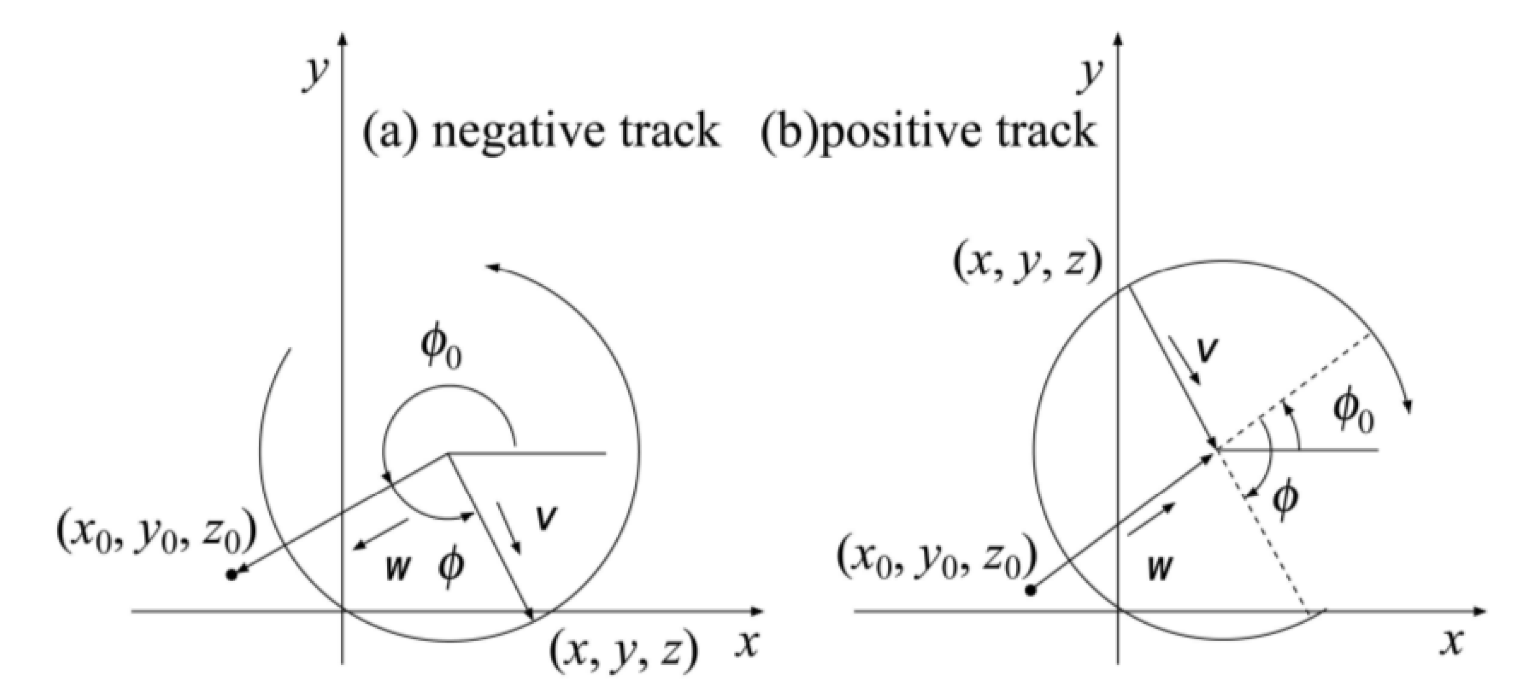
5.4.2. Track Reconstruction

The trajectory of a charged particle in a homogeneous, solenoidal magnetic field, and in a region where the material budget is low can be approximated mathematically with a helix coaxial to the magnetic field direction. The helix is fully defined by five parameters ( d ρ , ϕ 0 , k , d z , tan λ ) where d ρ is the signed distance in radial direction with respect to the pivot point ( x 0 , y 0 , z 0 ) , ϕ 0 is the azimuth angle which pinpoints the pivot with respect to the axis of the helix, k is the curvature of the helix, d z is the signed distance in axial direction with respect to the pivot, and λ = π 2 θ (with θ as the polar angle) is the so-called dip angle (see Figure 21). The origin of the axes is often chosen as the pivot point.
Track reconstruction foresees two steps: pattern recognition and track fitting. The CGEM-IT clusters and the ODC hits must be at first grouped to find suitable track candidates and then fitted to extract the helix parameters.
As the full MDC already has a complete pattern recognition based on Hough Transformation [82], two methods have been developed to associate the clusters to the correct track candidate. The first method, called Track Segment Finder [83], is an algorithm to find the CGEM-IT tracklets using this detector alone and then match the track segments with the ones found by the independent ODC pattern recognition. The second method, called Hough Track Finder [84], uses the whole tracking system at once, including CGEM-IT and ODC, and acts on all the hits in a global mode. Once the pattern recognition is completed, the track is fitted with the Kalman filter algorithm [70]. All these algorithms are validated with MC samples.
Track Segment Finder—This algorithm extracts a set of variables to identify the tracklet by starting from a MC simulation of muons with different momenta from 50 MeV/c to 1 GeV/c; the MC coordinates ( ϕ i , z i ) of the points on each of the CGEM-IT layers are considered and the following differences are computed:
δ ϕ 21 = ϕ 1 ϕ 2 ,
δ ϕ 23 = ϕ 3 ϕ 2 ,
δ z 21 = z 1 z 2 ,
δ z 23 = z 3 z 2 .
The plots δ ϕ 21 vs. δ ϕ 23 and δ z 21 vs. δ z 23 identify the correct relations between the coordinates of the points belonging to a track. When considering the three-cluster combinations, the right ones can be identified and the wrong ones can be discarded. The efficiency of this method exceeds 99% for the whole range of muon momenta, as shown in Figure 22. The found tracklet is then fitted via the Least Square Method and an helix track hypothesis. It is finally matched to the tracklets found by the dedicated pattern recognition in the ODC alone by computing the χ m a t c h 2 on each of the helix parameters H:
χ m a t c h 2 = ( H C G E M I T H O D C ) 2 σ C G E M I T 2 σ O D C 2 .
A cut on the χ m a t c h 2 is applied to select the matched tracks.
Hough Track Finder—The second track finding method uses the information from the CGEM-IT together with the one from the ODC and applies the Hough Transformation to all the hits at once.
The Hough Transformation [85] is a method widely used in pattern recognition problems and originally applied in BESIII to the MDC, particularly for low momentum particles [82].
The hits belonging to a helix track lie on a circle when projected in the transverse plane. The coordinates x , y in the real transverse plane are transformed into the coordinates X , Y in the conformal plane by the Conformal Transformation:
X = 2 x x 2 + y 2 ,
Y = 2 y x 2 + y 2 .
A circle passing through the origin of the axes in the real x y plane is transformed into a straight line in the X Y conformal plane, while the drift circles, i.e., the circles reconstructed in the ODC from the measured drift time in the real plane, are transformed into another circles, tangent to the straight line in the conformal plane.
The straight line which identifies the track in the conformal plane is transformed into a point in the Hough parameter plane by the application of another geometrical transformation, the Hough Transformation:
ρ = X cos α + Y sin α ,
where ( ρ , α ) are the straight line parameters. Instead, the drift circles in the conformal plane are transformed into sinusoidal curves in the parameter plane, by the Legendre Transformation, a particular Hough Transformation:
ρ = X 0 cos α + Y 0 sin α ± r ,
where ( X 0 , Y 0 ) is the center of the drift circle and r is its radius.
The pattern recognition consists in finding the point where different sinusoidal curves cross, which represents the parameters of the track tangent to all the drift circles (see Figure 23), hence the original helix track, once the parameters are transformed back to the real x y plane.
Kalman filter—The output of the track finder step is the list of hits associated to a track candidate and a preliminary track parameter reconstruction, obtained with a global fit of the hits with the helix hypothesis. This fit does not take into account either the multiple scattering or the possible non-homogeneity of the magnetic field, hence the track candidate is usually fitted once again with a local, iterative algorithm, the Kalman filter. This method updates the track hypothesis on each detector plane with a weighted average of the extrapolated position of the track, starting from the previous plane, and of the measured hit position. In [70] a preliminary estimate of the track resolution with the system CGEM-IT + ODC compared to the system IDC + ODC is reported, as shown in Figure 24, with a simulation of single muon events with a momentum of 1 GeV/c. The vertex resolution in the x y plane obtained with the CGEM-IT solution is compatible with the one from the full MDC solution (Figure 24a), as well as the momentum resolution (Figure 24c), while a relevant improvement is expected in the vertex z coordinate reconstruction (Figure 24b). These results have been obtained without pattern recognition as only one track per event was simulated and with an adaptation of the Kalman filter routines to accommodate the three points reconstructed on the CGEM-IT layers in the algorithm, together with the ODC points. The CGEM-IT geometry is the same as the simulated one.

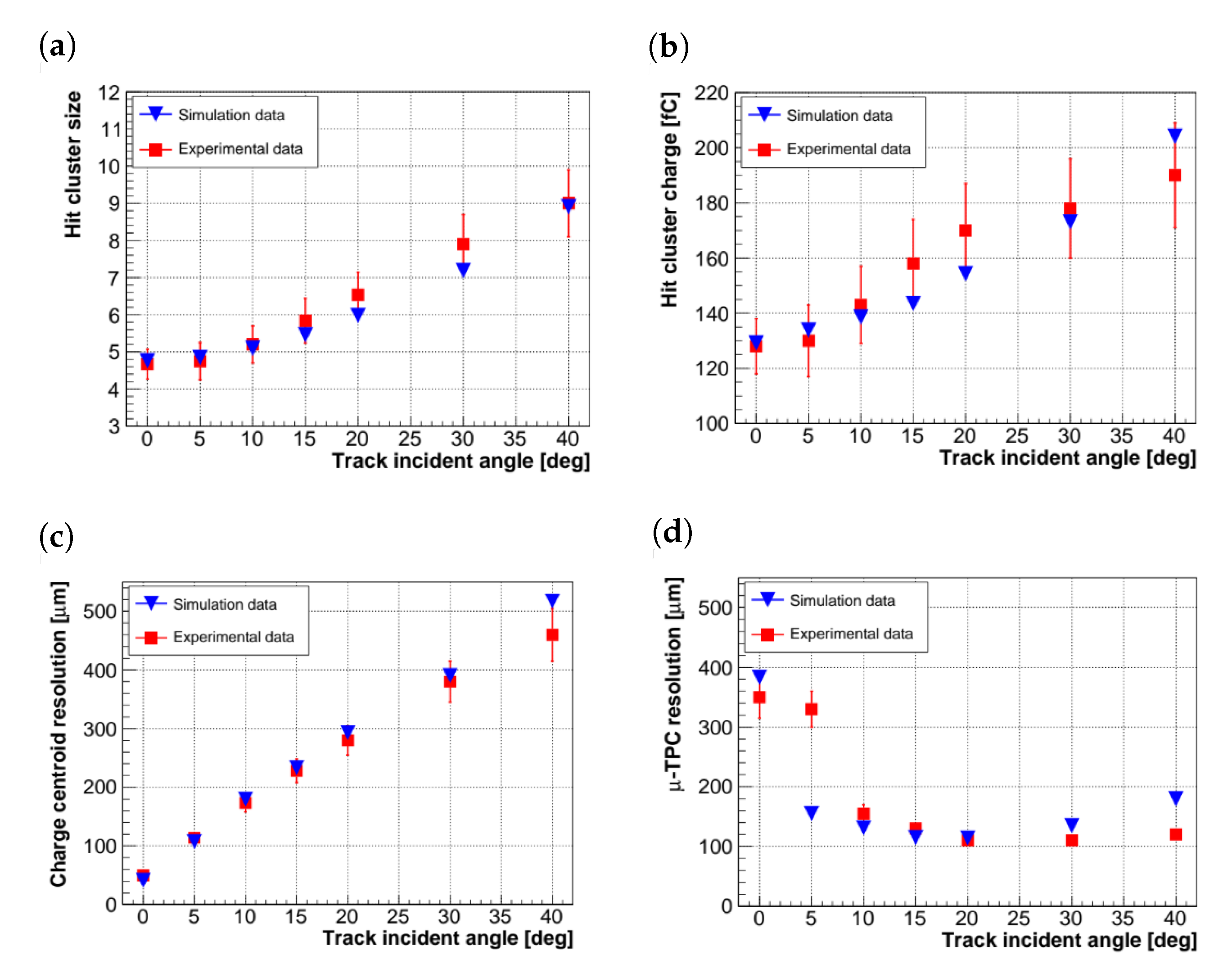
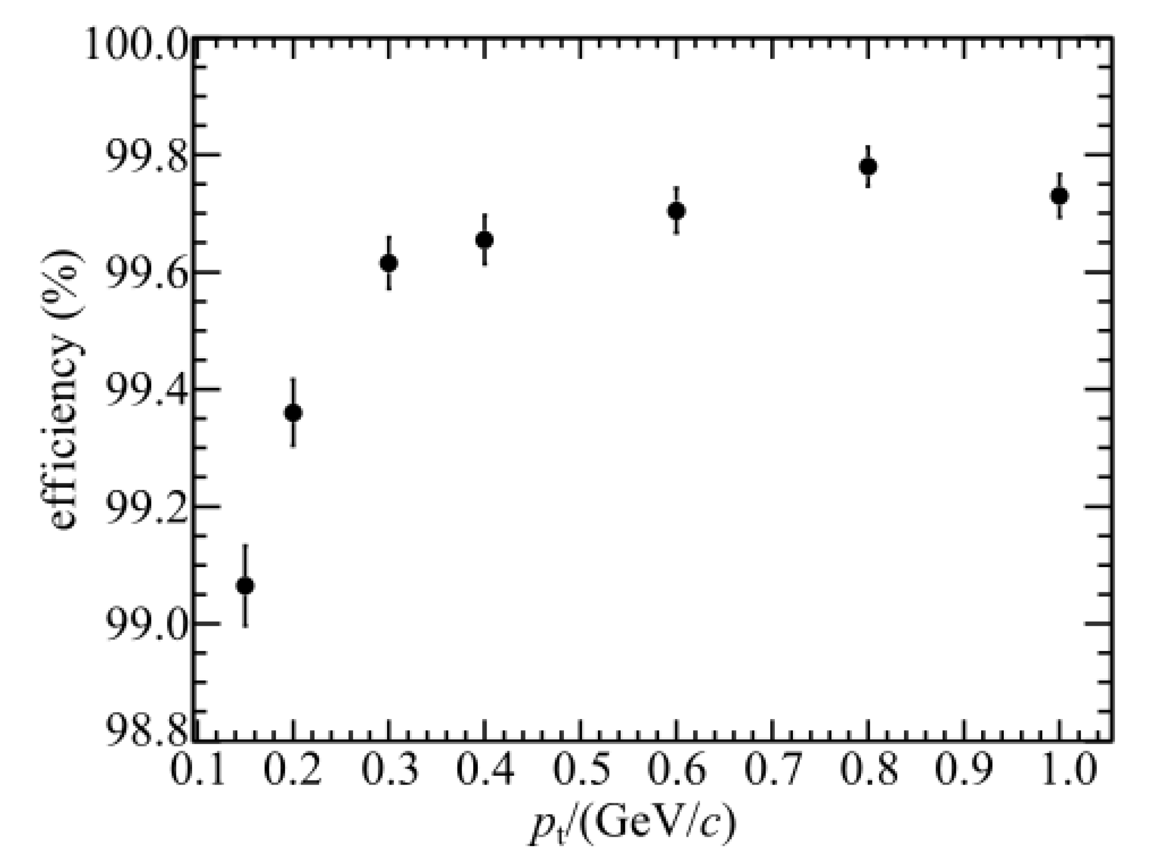
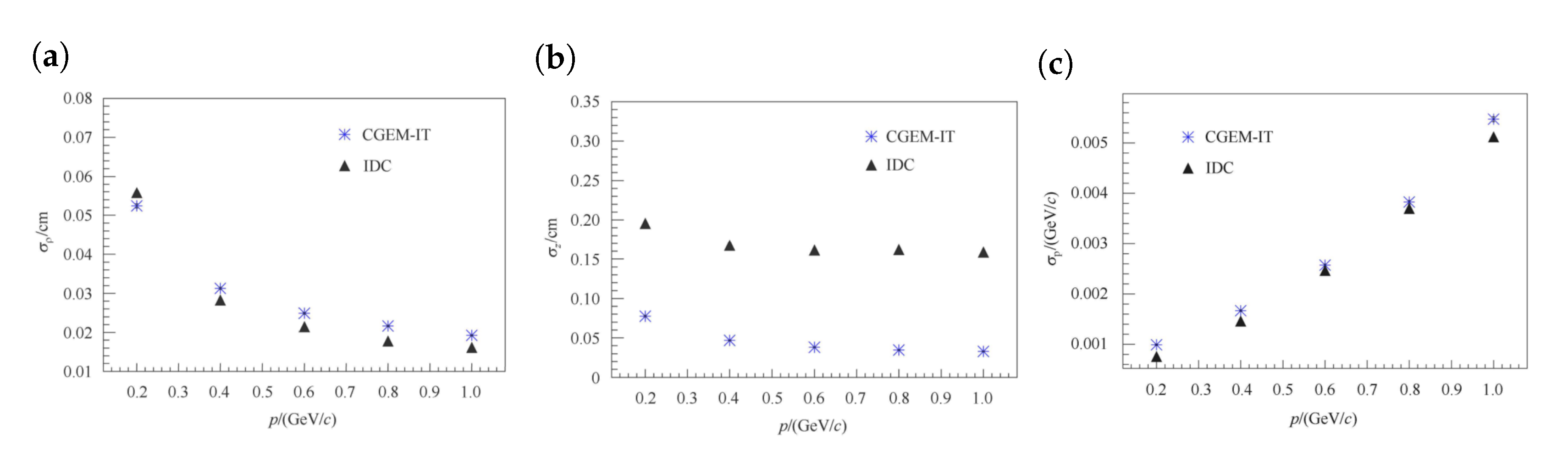
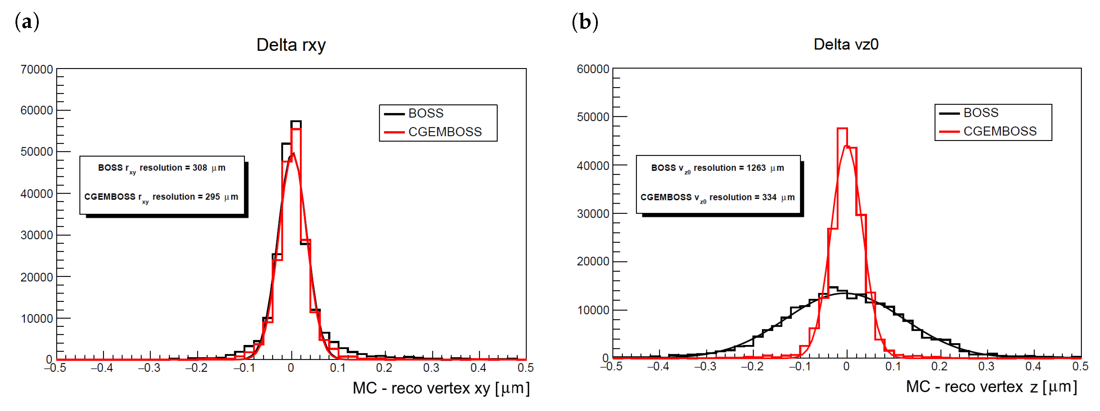
5.5. Evaluation of the Performance with Benchmarks

The impact of the replacement of the IDC with the CGEM-IT has been evaluated with a physics analysis of the benchmark channel e + e J / ψ π + π π 0 with π 0 γ γ [33].
Five hundred thousand events have been generated and simulated in BOSS with the complete MDC geometry and in CgemBOSS with the CGEM-IT and the ODC setup. The same reconstruction procedure and selection cuts have been applied, in order to compare the different trackers only. The selection of events has been performed, requiring two charged tracks pointing to the same vertex within 1 cm in the radial direction and 10 cm along the beam line and a pair of photons with invariant mass around the π 0 mass. Additionally the invariant mass of the three found pions has been constrained to the J / ψ mass by a kinematic fit.
The resulting resolutions on the J / ψ vertex position both in x y plane and in the axial z coordinate are shown in Figure 25a,b respectively, both for the MDC and for CGEM-IT + ODC. As expected, the resolution in the transverse plane stays the same around 300 µm, while an evident improvement shows up in the coordinate along the beam direction. The resolution in this case improves from 1.2 mm for the MDC to 350 µm with the new setup, thanks to the larger stereo angles: the tilted wires of the MDC have in fact angles in the range [−3.4°, +3.9°], while the V strips of the CGEM-IT have the stereo angles equal to +46.7°, −31.0° and +32.9° on the inner, middle, and outer layer, respectively (see Table 1).
The larger stereo angles will have a major impact on the reconstruction of displaced vertices, i.e., the decay vertices of long-living neutral particles as the Λ and the K s 0 . A toy MC that takes into account the expected improvement in the z coordinate reconstruction was used to evaluate how the better z resolution will influence the resolution of the reconstructed position of the vertex. An improvement in the vertex position resolution of a factor of two or three is expected [35].

6. CGEM-IT Testing and Commissioning

Characterization of the CGEM-IT for BESIII began in 2014 with small planar triple-GEM prototypes interfaced to the APV-25 electronics [79]. Once the first CGEM-IT production was ready, two cylindrical triple-GEMs were characterized with the same electronics in 2016 (middle layer) and 2017 (inner layer). Following the electronics developments, new studies were performed with TIGER readout on a planar triple-GEM detector in 2018. Since 2019, the full characterization of the TIGER/GEMROC readout of the final layers of the CGEM-IT has been performed to verify that the BESIII requirements indicated in Table 2 have been met.

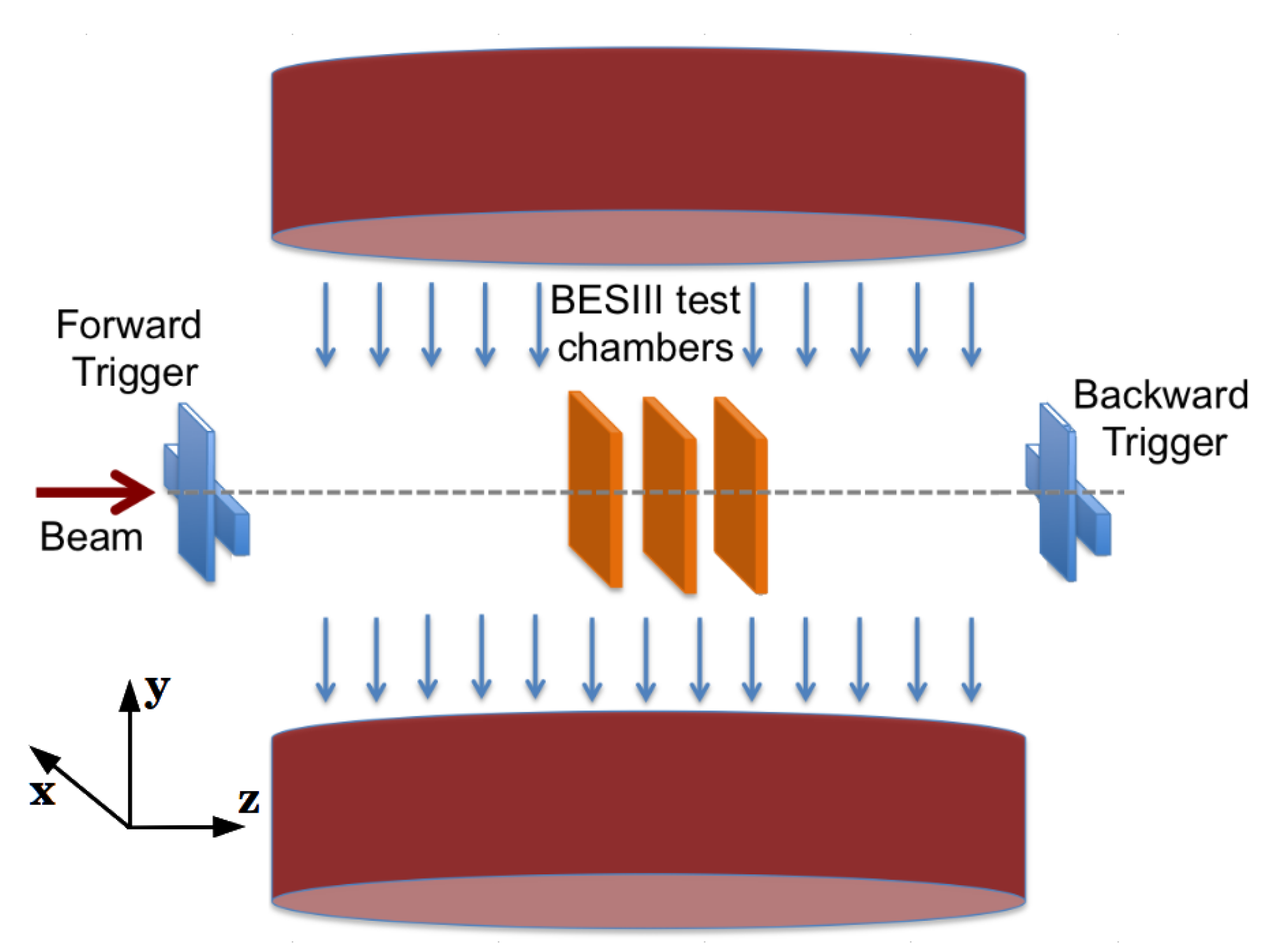
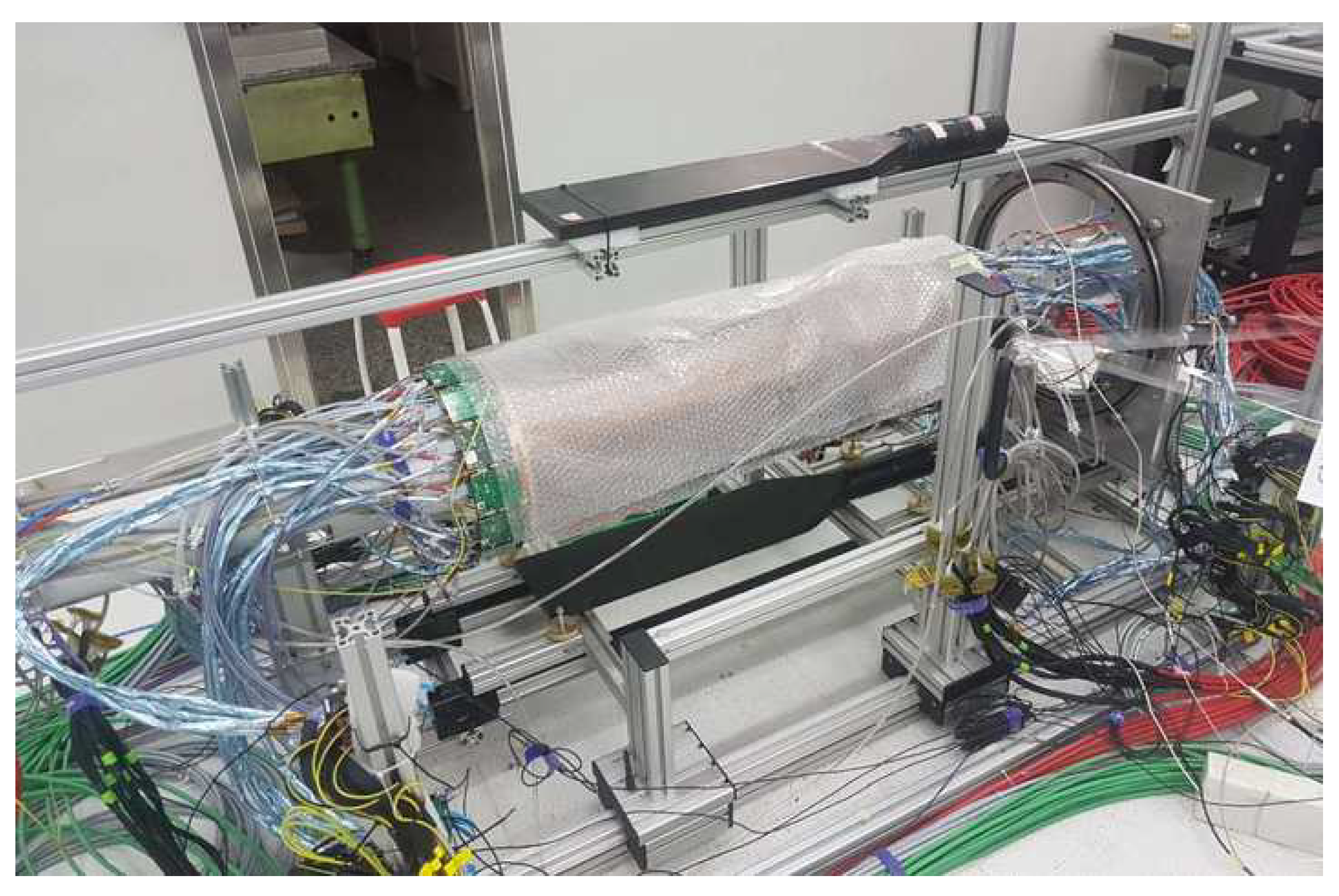
6.1. Test Facility and Test Setup

Characterization of the detector was performed with cosmic rays and beams of muons and pions at the SPS-H4 line test beam facility at CERN North-Area [86]. Here, a beam of muons or pions is provided with momentum up to 180 GeV/c. In the experimental area available to the RD51 collaboration [87,88] at the H4 beam line, the world’s largest ferromagnetic dipole magnet, Goliath [89], with a magnetic field up to 1.5 T in both polarities, can be used with a magnetic field orthogonal to the electric field of the triple-GEM similar to the BESIII environment. The setup used in the characterization always consists of the detector under test and a tracking system to select good tracks and to evaluate efficiency and position resolution. An example of a test setup is shown in Figure 26. The beam direction, in case of a testbeam, or the vertical one, in case of cosmic ray tests, defines the z axis, while the x y plane coincides with the anode; if the magnetic field is present, the x axis is the one perpendicular to B while the y axis is parallel to B. The direction of the incident particle is parallel to the electric field E and perpendicular to the GEM plane. Some of the proposed validation measurements are performed with a rotation of the detectors around their vertical axis to characterize them with inclined tracks. A trigger system with two scintillator bars read by photomultiplier tubes are placed; one upstream and the other downstream of the setup.
Both the prototypes and the CGEM-IT have a bi-dimensional readout. In the following characterization, only one view will be considered to simplify the analysis but the results can be applied to both views. The data collected are reconstructed using the procedure described in Section 5.4 with the CgemBOSS framework [90], for the CGEM-IT validation, and by using a stand-alone code called GRAAL [91], for the planar triple-GEMs. Algorithms that take care of reconstruction, alignment and analysis have been applied.

6.2. Triple-Gem Characterization

A digital readout is used in the cylindrical GEM for KLOE-2 and, there, the spatial resolution is limited to the cluster size divided by 12 . The analogue readout provides charge and time information for each strip collecting a signal above threshold and this extends the possible reconstruction techniques. Once the charged particles ionize the gas mixture in the detector, the electrons diffuse in the gas from the point of origin to the anode. The number of electrons collected at the anode is set through the three amplification stages.

6.2.1. Planar Triple-GEM Signal Shape

The first point to be studied is the correlation between the gain and the signal shape. Figure 27a shows the one-dimensional cluster size and cluster charge: both variables increase with the gain and their behavior depends on the gas mixture [33]. The mean cluster charge in Ar:iC 4 H 10 (90:10) gas mixture is larger due to a slightly larger ionization compared to Ar:CO 2 (70:30) gas mixture. The difference in cluster size is dominated by the electron transverse diffusion, which is about twice as large in Ar:iC 4 H 10 gas mixture.
The signal shape is determined mainly by the detector gain, the gas mixture, and even a geometrical factor: the impinging angle of the particle on the detector. It defines the ionizing path and the spatial distribution of the primary electrons: the larger the angle, the larger the track length in the drift gap where the ionization takes place and the higher is the number of primary electrons. Charge and time distributions are strongly related to the impinging angle and this affects the reconstruction algorithms and their spatial resolution. If the tracks are orthogonal to the GEM plane, defined as 0 , then the initial position of the primary electrons differs only in the drift direction, while for angles that deviate from 0 the spatial distribution of the charge is spread on more strips, thus resulting in a increased cluster size. This effect is reported in Figure 27b and in the tuning results in Figure 19a,b.

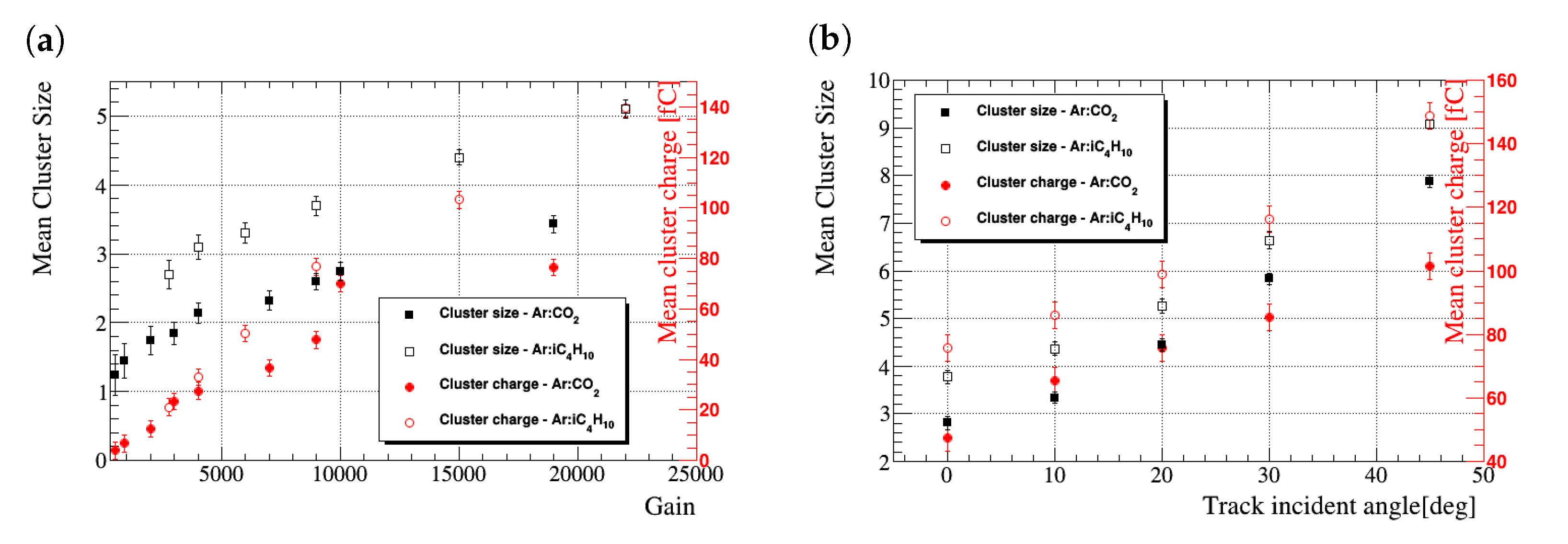
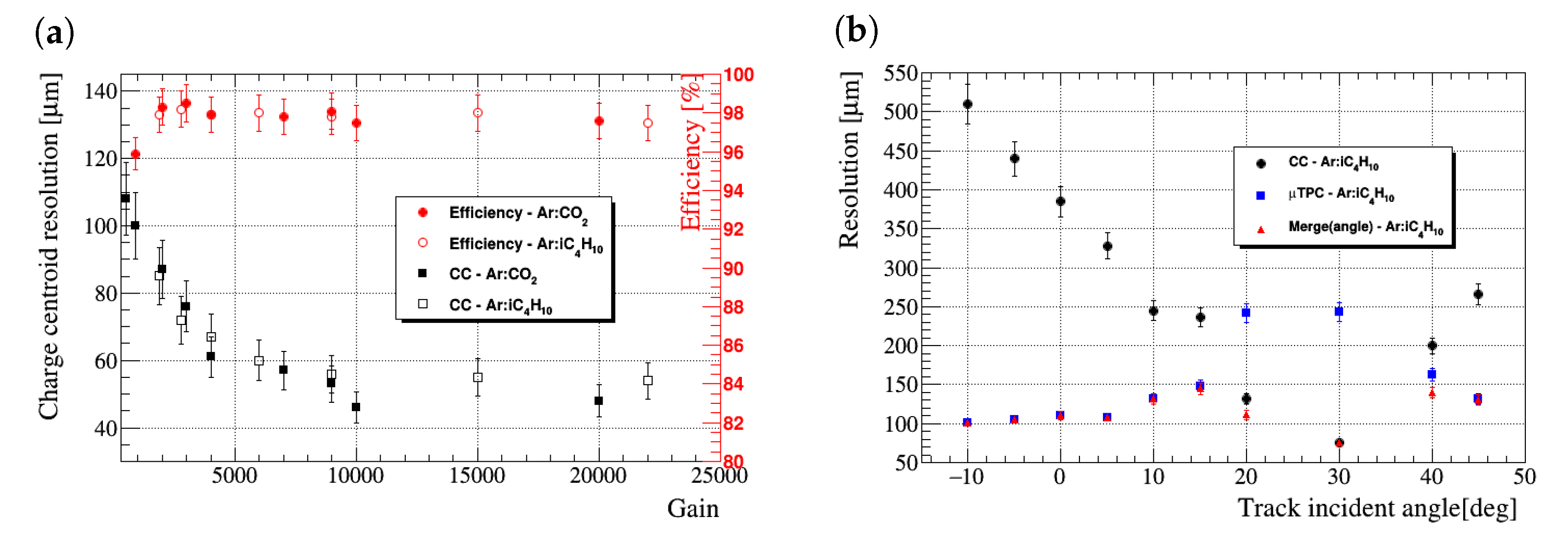
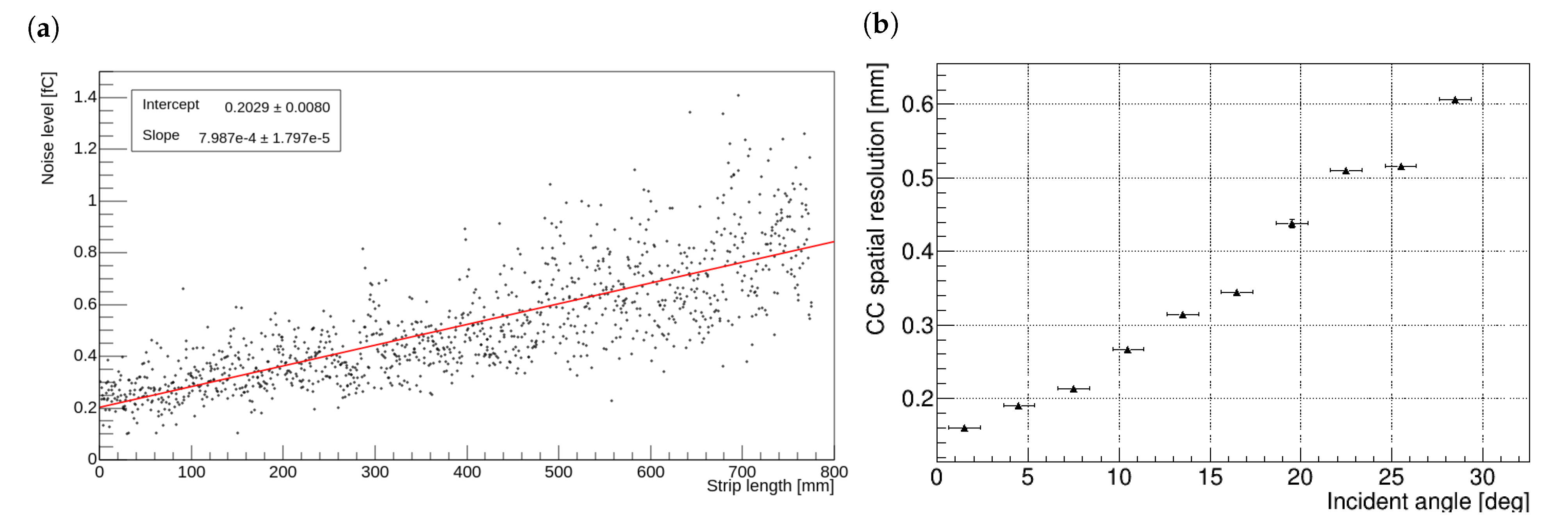
6.2.2. Planar Triple-GEM Efficiency and Spatial Resolution

Following the signal shape characterization, the detector efficiency and its spatial resolution are studied to find the optimal parameters. Figure 28a shows efficiency and CC resolution as a function of the gain: once the gain reaches 2000, then the efficiency reaches the plateau of 98% while a spatial resolution of 50 µm is measured at a gain of 10,000. Once the working point is set, the reconstruction algorithms are evaluated. As mentioned earlier, CC and µTPC are anti-correlated algorithms. Since the cluster size increases at larger angles, the path within the ionization gap can be properly reconstructed and the µTPC resolution improves significantly, as shown by the tuning results in Figure 19a,b. Under these conditions the charge distribution is no longer Gaussian and the CC worsens its performance.
When orthogonal tracks are considered and the magnetic field is turned on, due to the Lorentz angle, an impact on the reconstructed tracks with a behavior similar to the impinging angle is observed. A combination of the Lorentz and impinging angles is necessary to understand the triple-GEM behavior in the BESIII configuration with 1 T magnetic field. If an Ar:iC 4 H 10 gas mixture and 1.5 kV/cm drift field are used, then a Lorentz angle of 26 is expected. When the impinging angle matches the Lorentz angle, a focusing effect occurs and the charge distribution remains Gaussian; when they differ, a defocusing effect spreads the charge on several strips and the signal is collected on a larger cluster size. This explains the results shown in Figure 28: around 26 the best performance is obtained with the CC while in the other regions the µTPC is the most efficient algorithm. A combination of the two, reported in Equation (8), ensures a stable spatial resolution throughout the region of interest [33,92,93].

6.2.3. Cylindrical Triple-GEM Validation

The inner and the middle layers of the first CGEM-IT production were studied in two separate testbeams at the SPS-H4 line at CERN to validate the performance of a triple-GEM with a cylindrical shape and with a detector much bigger than the planar prototypes. The challenges of this measurement involve both the HV stability of the detector and the signal readout. Characterization as a function of gain and incident angle was performed for the CGEM. The results showed a correlation between the cluster charge and cluster size similar to the planar GEM, hence the signal shape is not significantly affected by the detector geometry and size. Regarding the resolution, only the CC was evaluated and the same behavior as for the planar GEM detector was observed as a function of the impinging angle [33].

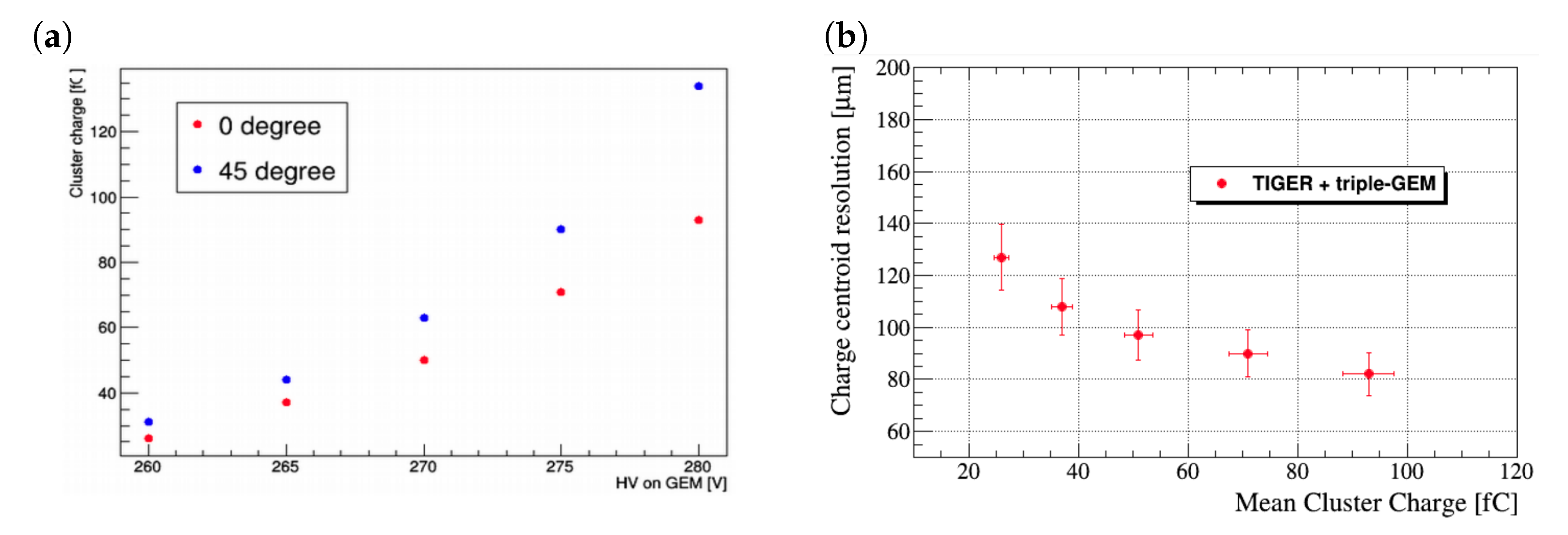
6.2.4. TIGER and Triple-GEM Validation

Integration between the TIGER chip and a planar triple-GEM detector was performed with a testbeam at the SPS-H4 line in 2018. In this testbeam, the TIGER chips were coupled to a different readout chain, based on a Virtex-6 FPGA evaluation board, since the GEMROC modules were not yet available. This readout was trigger-less, therefore a different approach to select only the data corresponding to the time window of interest was adopted. The trigger signal coming from the coincidence of the scintillators was injected on one TIGER channel directly to the TDCs and then the digitized output of that channel was used in the offline analysis to retrieve the trigger time information and thus assign each data to the corresponding trigger signal [23,33]. The cluster charge for different gain settings and the spatial resolution of the CC are displayed in Figure 29 and show a trend similar to one obtained from the previous electronics.

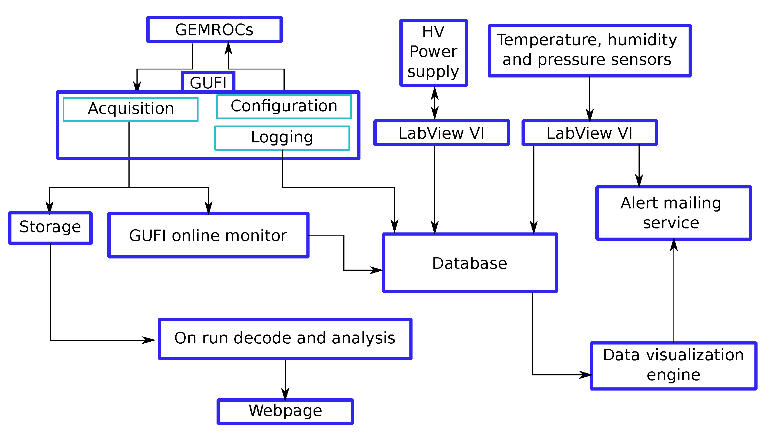
6.3. CGEM-IT Commissioning

The deployment of the CGEM-IT and its readout system started in late 2018 and is ongoing at IHEP, in a dedicated laboratory. A cosmic ray setup, which includes two of the three CGEM layers, has been assembled and is used to monitor the detector, test, and debug the electronics readout chain and measure the system performance and stability. A picture of the setup is shown in Figure 30. The inner and middle layers are already assembled, one inside the other, as in the final BESIII experiment. The detectors are flushed with an Ar:iC 4 H 10 (90:10) gas mixture and operated at a gain of 10,000–12,000, with the electric fields between the electrodes set to 1.5/3/3/5 kV/cm (from cathode to anode). In this setup, the coincidence of plastic scintillator detectors placed above and below the CGEM-IT generates the trigger signal, which is fed to the GEMROC modules for the trigger-matching operations to select and fully reconstruct data from cosmic rays interacting with both CGEM layers.
The system can be remotely controlled using several tools [21] providing functionalities not only to run the acquisition but also to monitor and log the setup conditions. The scheme of the full software system is shown in Figure 31 and includes the following features:
  • The detector HV is controlled by a LabVIEW [94] program, which allows the user to set the electrodes voltage and monitor the absorbed currents;
  • The gas flux of Ar and iC 4 H 10 is measured by two flow meters read by an Arduino [95] microcontroller, which is interfaced with a LabVIEW program;
  • The temperature and humidity of the room are monitored by commercial sensors and read with another Arduino microcontroller and LabVIEW program;
  • The current absorption and operating temperature of the on-detector electronics are read directly by the GEMROC modules and stored.
These variables are saved in an Influx-DB database [96] and can be visualized via the Grafana interface [97], which also provides an automatic alert service in case the value of any of these parameters is out of range. In addition, the software can perform a fast online analysis, using part of the acquired data, to extract several key features and assess the status of the detector and the electronics, as shown in Figure 32. All these features allowed the CGEM-IT BESIII community to continue to operate the system after the SARS-CoV-2 outbreak.
Threshold scans are periodically run on all channels to check the status of the entire setup. The on-chip test pulse is used to measure the system noise levels and check the stability of the readout chain. The results from this scan are displayed in Figure 33a. The noise is almost constant, around 1 fC, for the longitudinal X strips, which share the same length, while for the stereo V strips, which have different lengths according to their position in the anode plane, the noise can range from 0.2 fC to 1 fC. From these measurements, thresholds are equalized using an automatic algorithm in such a way that all channels have a similar noise occupancy, typically between 5 and 8 kHz.
This setup has been taking data since December 2019, testing the readout chain reliability and stability, while providing data for the development and the calibration of the analysis software.
A cosmic ray interacting with the setup generates four bi-dimensional clusters, two for each layer. Three points are used to reconstruct the track while the fourth is used to test the detector. The average cluster charge and cluster size are monitored since December 2019 and the reconstruction algorithms CC, µTPC, and merge are under characterization. As reported in Figure 33b, the CC resolution as a function of the incident angle of the tracks behaves as expected, even if the tracking system contribution has not been subtracted yet in the current analysis [90]: if the incident angle is 0 , a residual of 100 µm is measured. The µTPC is a more complex and delicate algorithm. The time calibrations of the CGEM-IT are ongoing and only preliminary results are available up to now, where an agreement between the µTPC and CC spatial resolutions is found.

7. Conclusions

The project for the new inner tracker based on the cylindrical triple-GEM technology, proposed for the BESIII upgrade, has been reviewed in this paper. The innovative solutions developed for this tracking system exploit the latest results in mechanics, electronics, and software fields. The refined and improved techniques allowed for the design and construction of a detector with a cylindrical shape and unprecedented performance, while keeping the mechanical structure light. More than 10,000 channels will be instrumented in the inner region of the BESIII spectrometer, around the beam pipe, to track the path of charged particles with a spatial resolution of 130 µm in the transverse plane and better than 350 µm along the beam direction, thus delivering a factor two to three improvement in the spatial resolution of the secondary vertices.
The detector characteristics have been specifically optimized to meet the requirements imposed by the BESIII experiment. A double view anode has been used in each of the three CGEM-IT layers to obtain three high resolution 3D measurements close to the interaction point. The optimal resolution on the position coordinate along the beam direction is achieved thanks to the large stereo angles of the tilted strips. A custom ASIC, performing charge and time measurements of the detector signals, has been developed to exploit the analogue readout and enable three methods for position reconstruction. The widely used charge centroid mode, powerful on orthogonal tracks, has been complemented by the µTPC mode. The latter provides a better resolution in the reconstruction of trajectories, which are inclined with respect to the electrode planes, travel a long path inside the drift gap and fire a large number of strips. The 5mm drift gap thickness was chosen for the application of this reconstruction method as it provides a sufficient number of hits for the µTPC. FPGA-based modules have been developed for the readout chain, to properly interface the on-detector electronics with the BESIII clock, trigger, and DAQ systems. The mechanical structure has been designed to ensure the detector robustness while keeping the material budget low. In fact, being the CGEM-IT in the central region of the spectrometer, all its materials must be light, so as not to deteriorate the particle paths to the external systems and not to produce an excess of background signals. The construction procedure, partly inherited from the KLOE-2 first cylindrical triple-GEM, was improved and updated to address the specific requirements of the CGEM-IT, which has different dimensions and also needs to be shipped from Italy to China.
Both the detector and the electronics have been tested to verify that they meet the specifications required by the BESIII experiment. The configuration settings have been optimized by means of several experimental tests, a long testbeam campaign and the in-depth study of the physics involved in this technology through MC simulations and the development of the reconstruction algorithms. To date, two of the three CGEM-IT layers are complete, while the third is under construction with a sandwich of carbon fiber and honeycomb to ensure a good robustness and a low material budget. The two existing layers have been assembled at IHEP and their final validation with the full readout chain has been ongoing since late 2019, with cosmic ray data taking. Since the SARS-CoV-2 outbreak, the cosmic ray telescope has been operated and controlled remotely. Any upgrades to the present CGEM-IT setup have been postponed until travel to China is permitted again.

Author Contributions

Writing—original draft preparation, I.B., F.C., R.F. and L.L.; writing—review and editing, I.B., F.C., R.F. and L.L. All authors have read and agreed to the published version of the manuscript.

Funding

This research was funded by the European Commission in the RISE Project 645664-BESIIICGEM, H2020-MSCA-RISE-2014 and in the RISE Project 872901-FEST, H2020-MSCA-RISE-2019.

Institutional Review Board Statement

Not applicable.

Informed Consent Statement

Not applicable.

Data Availability Statement

The data used in this study can be provided by the authors upon reasonable request.

Acknowledgments

The authors would like to thank the BESIII Collaboration and acknowledge the researchers from INFN, IHEP, and Institutes from Indiana, Mainz, and Uppsala Universities participating in the CGEM-IT project, whose work has been reviewed in this paper. The authors are also immensely grateful to the IHEP colleagues who helped with their assistance in the CGEM-IT maintenance during the SARS-CoV-2 pandemic, which forced the collaboration to operate the system remotely given the travel restrictions to China.

Conflicts of Interest

The authors declare no conflict of interest.

Abbreviations

The following abbreviations are used in this manuscript:
ADCAnalogue-to-Digital Converter
ASICApplication Specific Integrated Circuit
BEPCIIBeijing Electron Positron Collider II
BESIIIBEijing Spectrometer III
BLHBaseline holding
BOSSBESIII Offline Software System
BOOSTBESIII Object-Oriented Simulation Tool
CERNConseil Européen pour la Recherche Nucléaire
CCCharge Centroid
CGEMCylindrical Gas Electron Multiplier
CMOSComplementary metal-oxide semiconductor
CSACharge sensitive amplifier
DACDigital-to-Analogue Converter
DDRDouble Data Rate
DLVPCData and Low Voltage Patch Card
DSTData Summary Tape
EMCElectro-Magnetic Calorimeter
ENCEquivalent Noise Charge
ETOFEnd-cap Time-Of-Flight
FEBFront-End Board
FPGAField Programmable Gate Array
GbEGigabit Ethernet
GDMLGeometry Description Markup Language
GEMGas Electron Multiplier
GEMDCGEM Data Concentrator
GEMROCGEM Read-Out Card
GRAALGem Reconstruction And Analysis Library
GUFIGraphical User Front-end Interface
HVHigh Voltage
IDCInner Drift Chamber
IHEPInstitute of High Energy Physics
INFNIstituto Nazionale di Fisica Nucleare
ITInner Tracker
LQCDLattice Quantum Chromo-Dynamics
LVLow Voltage
MCMonte Carlo
MDCMain Drift Chamber
MPGDMicro Pattern Gas Detector
µTPCmicro Time Projection Chamber
MRPCMulti-gap Resistive Plate Chamber
MUCMUon Counter
ODCOuter Drift Chamber
PLLPhase-locked loop
QCDQuantum Chromo-Dynamics
S&HSample-and-Hold
SDRSingle Data Rate
SMStandard Model
SSMSuperconducting Solenoid Magnet
TACTime-to-Amplitude Converter
TDCTime-to-Digital Converter
TIDTotal Ionizing Dose
TIGERTorino Integrated Gem Electronics for Readout
TOFTime-Of-Flight
ToTTime-over-Threshold
UDPUser Datagram Protocol
VIMVertical Insertion System
VMEVersa Module Eurocard
YBCOYttrium Barium Copper Oxide

References

  1. Ablikim, M.; An, Z.H.; Bai, J.Z.; Niklaus Berger, J.M.; Bian, J.M.; Cai, X.; Cao, G.F.; Cao, X.X.; Chang, J.F.; Chen, C.; et al. Design and Construction of the BESIII Detector. Nucl. Instrum. Methods Phys. Res. Sect. A 2010, 614, 345. [Google Scholar] [CrossRef] [Green Version]
  2. Zhang, C.; Pei, G.X. BEPCII: The second phase construction of the Beijing Electron-Positron Collider. In Proceedings of the 2005 Particle Accelerator Conference, Knoxville, TN, USA, 16–20 May 2005. [Google Scholar] [CrossRef] [Green Version]
  3. Karliner, M.; Rosner, J.L.; Skwarnicki, T. Multiquark States. Annu. Rev. Nucl. Part. Sci. 2018, 68, 17–44. [Google Scholar] [CrossRef] [Green Version]
  4. Choi, S.K.; Olsen, S.L.; Abe, K.; Abe, T.; Adachi, I.; Byoung, S.A.; Aihara, H.; Akai, K.; Akatsu, M.; Akemoto, M.; et al. Observation of a Narrow Charmonium-like State in Exclusive B±K±π+πJ/ψ Decays. Phys. Rev. Lett. 2003, 91, 262001. [Google Scholar] [CrossRef] [PubMed] [Green Version]
  5. Aubert, B.; Barate, R.; Boutigny, D.; Couderc, F.; Karyotakis, Y.; Lees, J.P.; Poireau, V.; Tisserand, V.; Zghiche, A.; Grauges, E.; et al. Observation of a Broad Structure in the π+πJ/ψ Mass Spectrum around 4.26 GeV/c2. Phys. Rev. Lett. 2005, 95, 142001. [Google Scholar] [CrossRef] [Green Version]
  6. Ablikim, M.; Achasov, M.N.; Ai, X.C.; Albayrak, O.; Ambrose, D.J.; An, F.F.; An, Q.; Bai, J.Z.; Baldini Ferroli, R.; Bhaghyesh, A.; et al. Observation of e+eγX(3872) at BESIII. Phys. Rev. Lett. 2014, 112, 092001. [Google Scholar] [CrossRef] [Green Version]
  7. Ablikim, M.; Achasov, M.N.; Ahmed, S.; Ai, X.C.; Albayrak, O.; Albrecht, M.; Ambrose, D.J.; Amoroso, A.; An, F.F.; An, Q.; et al. Precise measurement of the e+eπ+πJ/ψ cross section at center-of-mass energies from 3.77 to 4.60 GeV. Phys. Rev. Lett. 2017, 118, 092001. [Google Scholar] [CrossRef] [Green Version]
  8. Ablikim, M.; Achasov, M.N.; Ai, X.C.; Albayrak, O.; Ambrose, D.J.; An, F.F.; An, Q.; Bai, J.Z.; Baldini Ferroli, R.; Ban, Y.; et al. Observation of a Charged Charmonium-like Structure in e+eπ+πJ/ψ at (s)=4.26 GeV. Phys. Rev. Lett. 2013, 110, 252001. [Google Scholar] [CrossRef] [Green Version]
  9. Ablikim, M.; Achasov, M.N.; Ai, X.C.; Albayrak, O.; Ambrose, D.J.; An, F.F.; An, Q.; Bai, J.Z.; Baldini Ferroli, R.; Ban, Y.; et al. Observation of a Charged Charmoniumlike Structure Zc(4020) and Search for the Zc(3900) in e+eπ+πhc. Phys. Rev. Lett. 2013, 111, 242001. [Google Scholar] [CrossRef] [Green Version]
  10. Ablikim, M.; Achasov, M.N.; Adlarson, P.; Ahmed, S.; Albrecht, M.; Aliberti, R.; Amoroso, A.; An, Q.; Anita; Bai, X.H.; et al. Observation of a Near-Threshold Structure in the K+ Recoil-Mass Spectra in e+eK+(Ds-D*0+Ds*-D0). Phys. Rev. Lett. 2021, 126, 102001. [Google Scholar] [CrossRef]
  11. Asner, D.M.; Barnes, T.; Bian, J.M.; Bigi, I.I.; Brambilla, N.; Boyko, I.R.; Bytev, V.; Chao, K.T.; Charles, J.; Chen, H.X.; et al. Physics Goal of BESIII. Int. J. Mod. Phys. A 2009, S1, 24. [Google Scholar] [CrossRef]
  12. Ablikim, M.; Achasov, M.N.; Adlarson, P.; Ahmed, S.; Albrecht, M.; Alekseev, M.; Amoroso, A.; An, F.F.; An, Q.; Bai, Y.; et al. Future Physics Programme of BESIII. Chin. Phys. C 2020, 44, 040001. [Google Scholar] [CrossRef]
  13. Yuan, C.Z.; Olsen, S.L. The BESIII physics programme. Nat. Rev. Phys. 2019, S1, 480–494. [Google Scholar] [CrossRef]
  14. Pakhlova, G.; Adachi, I.; Aihara, H.; Arinstein, K.; Aulchenko, V.; Aushev, T.; Bakich, A.M.; Balagura, V.; Bedny, I.; Bhardwaj, V.; et al. Observation of a Near-Threshold Enhancement in the e+e → Λcc- Cross Section Using Initial-State Radiation. Phys. Rev. Lett. 2000, 101, 172001. [Google Scholar] [CrossRef] [Green Version]
  15. Ablikim, M.; Achasov, M.N.; Ahmed, S.; Albrecht, M.; Alekseev, M.; Amoroso, A.; An, F.F.; An, Q.; Bai, J.Z.; Bai, Y.; et al. Precision Measurement of the e+e → Λc+Λ¯c- Cross Section Near Threshold. Phys. Rev. Lett. 2018, 120, 132001. [Google Scholar] [CrossRef] [Green Version]
  16. Raimondi, P. Status at Super B Effort. Talk Presented at the 2nd Workshop on Super B-Factory, LNF-INFN, Frascati, Italy. 2006. Available online: http://www.lnf.infn.it/conference/superb06/talks/raimondi1.ppt (accessed on 31 January 2022).
  17. Bogomyagkov, A. Possibilities of Crab Waist. Talk Presented at the 14th International Workshop on Tau Lepton Physics, IHEP, Beijing, China. 2016. Available online: https://indico.ihep.ac.cn/event/5221/session/7/contribution/29/material/slides/0.pdf (accessed on 31 January 2022).
  18. Cao, P.; Chen, H.F.; Chen, M.M.; Dai, H.L.; Heng, Y.K.; Ji, X.L.; Jiang, X.S.; Li, C.; Li, X.; Liu, B.S.; et al. Design and construction of the new BESIII endcap Time-of-Flight system with MRPC Technology. Nucl. Inst. Methods Phys. Res. A 2020, 953, 163053. [Google Scholar] [CrossRef]
  19. Dong, M.Y. The BESIII and Its Upgrade, 30 Years of BES Physics. In Proceedings of the Symposium on 30 Years of BES Physics, Institute of High Energy Physics, Beijing, China, 5–6 September 2019; pp. 169–175. [Google Scholar] [CrossRef]
  20. Dong, M.Y.; Xiu, Q.L.; Wu, L.H.; Wu, Z.; Qin, Z.H.; Shen, P.; An, F.F.; Ju, X.D.; Liu, Y.; Zhu, K.; et al. Aging effect in the BESIII drift chamber. Chin. Phys. C 2016, 40, 016001. [Google Scholar] [CrossRef] [Green Version]
  21. Amoroso, A.; Baldini Ferroli, R.; Balossino, I.; Bertani, M.; Bettoni, D.; Bianchi, F.; Bortone, A.; Bugalho, R.; Calcaterra, A.; Cerioni, S.; et al. The CGEM-IT readout chain. JINST 2021, 16, P08065. [Google Scholar] [CrossRef]
  22. Xie, Y.J.; Qin, Z.H.; Ma, X.Y.; Zhang, J.; Wu, L.H.; Xie, W.; Dong, M.Y.; Dong, J.; Ji, X.L.; Jiang, X.S.; et al. Construction and cosmic-ray test of the new inner drift chamber for BESIII. Chin. Phys. C 2016, 40, 096003. [Google Scholar] [CrossRef]
  23. Cossio, F. A mixed-Signal ASIC for Time and Charge Measurements with GEM Detectors. Ph.D. Thesis, Politecnico di Torino, Torino, Italy, 2019. Available online: http://hdl.handle.net/11583/2743335 (accessed on 2 March 2022).
  24. Sauli, F. GEM: A new concept for electron amplification in gas detectors. Nucl. Instrum. Methods Phys. Res. A 1997, 386, 2–3. [Google Scholar] [CrossRef]
  25. Bencivenni, G.; Branchini, P.; Ciambrone, P.; Czerwinski, E.; De Lucia, E.; Di Cicco, A.; Domenici, D.; Felici, G.; Fermani, P.; Morello, G. The cylindrical GEM detector of the KLOE-2 experiment. JINST 2017, 12, C07016. [Google Scholar] [CrossRef]
  26. Gramigna, S. A Cylindrical GEM Inner Tracker for the BESIII Experiment: From Construction to Electronic Noise Studies. Master’s Thesis, University of Ferrara, Ferrara, Italy, 2021. Available online: https://jinst.sissa.it/jinst/theses/2021_JINST_TH_004.pdf (accessed on 31 January 2022).
  27. Sauli, F. The gas electron multiplier (GEM): Operating principles and applications. Nucl. Instrum. Methods Phys. Res. A 2016, 805, 2–24. [Google Scholar] [CrossRef]
  28. Bachmann, S.; Bressan, A.; Capeans, M.; Deutel, M.; Kappler, S.; Ketzer, S.; Polouektov, A.; Ropelewski, L.; Sauli, F.; Schulte, E.; et al. Discharge studies and prevention in the gas electron multiplier (GEM). Nucl. Instrum. Methods Phys. Res. A 2002, 479, 294–308. [Google Scholar] [CrossRef] [Green Version]
  29. Sauli, F. Principles of Operation of Multiwire Proportional and Drift Chambers. CERN 1975–1976. Available online: https://cds.cern.ch/record/117989 (accessed on 31 January 2022).
  30. Ketzer, B.; Ehlers, J.; Friedrich, J.; Grube, B.; Kapples, S.; Konorov, I.; Paul, S.; Placci, A.; Ropelewski, L.; Sauli, F. A fast tracker for COMPASS based on the GEM. Nucl. Phys. B Proc. Suppl. 2003, 125, 368–373. [Google Scholar] [CrossRef]
  31. Alfonsi, M.; Bencivenni, G.; Bonivento, W.M.; Cardini, A.; de Simone, P.; Murtas, F.; Pinci, D.; Poli Lener, M.; Raspino, D.; Saitta, B. The triple-GEM detector for the M1R1 muon station at LHCb. In Proceedings of the IEEE Nuclear Science Symposium, Fajardo, PR, USA, 23–29 October 2005; Volume 2, pp. 811–815. [Google Scholar]
  32. Fenker, H.C.; Burkert, V.; Ent, R.; Baillie, N.; Evans, J.; Fersch, R.; Griffioen, K.; Bradshawm, P.; Bueltmann, S.; Dodge, G. BoNuS: Development and Use of a Radial TPC using Cylindrical GEMs. Nucl. Instrum. Methods. Phys. Res. A 2008, 592, 273–286. [Google Scholar] [CrossRef]
  33. Farinelli, R. Research and Development in Cylindrical Triple-GEM Detector with µTPC Readout for the BESIII Experiment. Ph.D. Thesis, University of Ferrara, Ferrara, Italy, 2019. Available online: https://jinst.sissa.it/jinst/theses/2019_JINST_TH_002.pdf (accessed on 31 January 2022).
  34. Alfonsi, M.; Baccaro, S.; Bencivenni, G.; Bonivento, W.; Cardini, A.; de Simone, P.; Murtas, F.; Pinci, D.; Lener, M.P.; Raspino, D.; et al. Studies of etching effects on triple-GEM detectors operated with CF4-based gas mixtures. IEEE Trans. Nucl. Sci. 2005, 52, 2872–2878. [Google Scholar] [CrossRef]
  35. Ablikim, M.; Achasov, M.N.; Ai, X.C.; Albayrak, O.; Albrecht, M.; Ambrose, D.J.; Amoroso, A.; An, F.F.; An, Q.; Astorino, F.; et al. Conceptual Design Report—BESIII Cylindrical GEM Inner Tracker, Version 1.0.1. Internal Note 2014. Available online: http://www.lnf.infn.it/esperimenti/bes3/bes3_tdr_cgem.pdf (accessed on 31 January 2022).
  36. Balossino, I. Cylindrical GEMs Mechanical Structure’s Investigations and Improvements for the BESIII Experiment. Talk Presented at the Forum on Tracking Detector Mechanics. 2021. Available online: https://indico.cern.ch/event/1017981/contributions/4348788/attachments/2247229/3811723/BALOSSINO_BESIII_FoTDM2021.pdf (accessed on 31 January 2022).
  37. Duarte Pinto, S.; Villa, M.; Alfonsi, M.; Brock, I.; Croci, G.; David, E.; de Oliveira, R.; Ropelewski, L.; van Stenis, M. Progress on large area GEMs. J. Instrum. 2009, 4, P12009. [Google Scholar] [CrossRef] [Green Version]
  38. Balossino, I.; Alexeev, M.; Amoroso, A.; Bagnasco, S.; Baldini Ferroli, R.; Bertani, M.; Bettoni, D.; Bortone, A.; Bianchi, F.; Calcaterra, A.; et al. Investigation and improvements of the mechanical structure of cylindrical GEMs for the BESIII experiment. arXiv 2020, arXiv:2005.06264. [Google Scholar] [CrossRef]
  39. Archilli, F.; Badoni, D.; Babusci, D.; Bencivenni, G.; Bini, C.; Bloise, C.; Bocci, V.; Bossi, F.; Branchini, P.; Budano, A.; et al. Technical Design Report of the Inner Tracker for the KLOE-2 experiment. arXiv 2010, arXiv:1002.2572. [Google Scholar]
  40. Garzia, I.; Bettoni, D.; Cibinetto, G.; Fioravanti, E.; Santoro, V.; Savrie, M.; Carassiti, V.; Melchiorri, M.; Farinelli, R.; Rinchiuso, L.; et al. A Cylindrical GEM Detector with Analog Readout for the BESIII Experiment. In Proceedings of the 3rd International Conference on Technology and Instrumentation in Particle Physics (TIPP 2014), Amsterdam, The Netherlands, 2–6 June 2014; p. 292. [Google Scholar]
  41. Mignone, M.; INFN Sezione di Torino, Turin, Italy. BES3 Front-End Board PCB. Personal communication, 2017. [Google Scholar]
  42. Da Rocha Rolo, M.D.; Alexeev, M.; Amoroso, A.; Baldini Ferroli, R.; Bertani, M.; Bettoni, D.; Bianchi, F.; Bugalho, R.; Calcaterra, A.; Canale, N.; et al. A custom readout electronics for the BESIII CGEM detector. JINST 2017, 12, 7–17. [Google Scholar] [CrossRef]
  43. Rivetti, A.; Alexeev, M.; Bugalho, R.; Cossio, F.; Da Rocha Rolo, M.D.; Di Francesco, A.; Greco, M.; Cheng, W.; Maggiora, M.; Marcello, S.; et al. TIGER: A front-end ASIC for timing and energy measurements with radiation detectors. Nucl. Instrum. Methods Phys. Res. A 2019, 924, 181–186. [Google Scholar] [CrossRef] [Green Version]
  44. De Geronimo, G.; Fried, J.; Li, S.; Metcalfe, J.; Nambiar, N.; Vernon, E.; Polychronakos, V. VMM1—An ASIC for Micropattern Detectors. IEEE Trans. Nucl. Sci. 2013, 60, 2314–2321. [Google Scholar] [CrossRef]
  45. Rivetti, A. CMOS: Front-End Electronics for Radiation Sensors, 1st ed.; CRC Press: Boca Raton, FL, USA, 2015; pp. 196–197. [Google Scholar] [CrossRef]
  46. De Geronimo, G.; Fried, J.; O’Connor, P.; Radeka, V.; Smith, G.; Thorn, C.; Yu, B. Front-end ASIC for a GEM based time projection chamber. IEEE Trans. Nucl. Sci. 2004, 51, 1312–1317. [Google Scholar] [CrossRef]
  47. Fairstein, E. Linear unipolar pulse-shaping networks: Current technology. IEEE Trans. Nucl. Sci. 1990, 37, 382–397. [Google Scholar] [CrossRef]
  48. De Geronimo, G.; O’Connor, P.; Grosholz, J. A CMOS baseline holder (BLH) for readout ASICs. IEEE Trans. Nucl. Sci. 2000, 1, 818–822. [Google Scholar] [CrossRef] [Green Version]
  49. Martoiu, S.; Rivetti, A.; Ceccucci, A.; Cotta Ramusino, A.; Chiozzi, S.; Dellacasa, G.; Fiorini, M.; Garbolino, S.; Jarron, P.; Kaplon, J.; et al. A pixel front-end ASIC in 0.13 µm CMOS for the NA62 experiment with on pixel 100 ps Time-to-Digital Converter. In Proceedings of the IEEE Nuclear Science Symposium and Medical Imaging Conference (NSS/MIC 2009), Orlando, FL, USA, 24 October–1 November 2009; pp. 55–60. [Google Scholar] [CrossRef]
  50. Dellacasa, G.; Garbolino, S.; Marchetto, F.; Martoiu, S.; Mazza, G.; Rivetti, A.; Wheadon, R. A 130 nm ASIC prototype for the NA62 Gigatracker readout. Nucl. Instrum. Methods Phys. Res. A 2011, 650, 115–119. [Google Scholar] [CrossRef]
  51. Da Rocha Rolo, M.D.; Bugalho, R.; Gonçalves, F.; Mazza, G.; Rivetti, A.; Silva, J.; Silva, R.; Varela, J. TOFPET ASIC for PET applications. JINST 2013, 8, C02050. [Google Scholar] [CrossRef]
  52. Di Francesco, A.; Bugalho, R.; Oliveira, L.; Pacher, L.; Rivetti, A.; Da Rocha Rolo, M.D.; Silva, J.; Silva, R.; Varela, J. TOFPET2: A high-performance ASIC for time and amplitude measurements of SiPM signals in time-of-flight applications. JINST 2016, 11, C03042. [Google Scholar] [CrossRef]
  53. Riceputi, E.; Gaioni, L.; Manghisoni, M.; Re, V.; Dinapoli, R.; Mozzanica, A. Total ionizing dose effects on CMOS devices in a 110 nm technology. In Proceedings of the 13th Conference on Ph.D. Research in Microelectronics and Electronics (PRIME 2017), Giardini Naxos, Italy, 12–15 June 2017; pp. 241–244. [Google Scholar] [CrossRef]
  54. Cossio, F.; Alexeev, M.; Bugalho, R.; Chai, J.; Cheng, W.; Da Rocha Rolo, M.D.; Di Francesco, A.; Greco, M.; Leng, C.; Li, H.; et al. Design and characterization of the readout ASIC for the BESIII CGEM detector. In Proceedings of the Topical Workshop on Electronics for Particle Physics (TWEPP-17), Santa Cruz, CA, USA, 11–14 September 2017; p. 044. [Google Scholar] [CrossRef] [Green Version]
  55. Cossio, F.; Alexeev, M.; Bugalho, R.; Chai, J.; Cheng, W.; Da Rocha Rolo, M.D.; Di Francesco, A.; Greco, M.; Leng, C.; Li, H.; et al. Design and performance of the TIGER front-end ASIC for the BESIII Cylindrical Gas Electron Multiplier detector. In Proceedings of the 2017 IEEE Nuclear Science Symposium and Medical Imaging Conference (NSS/MIC 2017), Atlanta, GA, USA, 21–28 October 2017; pp. 1–3. [Google Scholar] [CrossRef] [Green Version]
  56. Altera Arria V FPGA Device Datasheet. Available online: https://www.intel.com/content/dam/www/programmable/us/en/pdfs/literature/hb/arria-v/av_51002.pdf (accessed on 31 January 2022).
  57. Liu, Z.; Gong, W.; Guo, Y.; Jin, D.; Li, L.; Lu, Y.; Qiao, Q.; Wang, K.; Wei, S.; Xu, H.; et al. Trigger System of BESIII. In Proceedings of the 2007 15th IEEE-NPSS Real-Time Conference, Batavia, IL, USA, 29 April–4 May 2007; pp. 1–4. [Google Scholar] [CrossRef]
  58. Branchini, P.; Budano, A.; Balla, A.; Beretta, M.; Ciambrone, P.; De Lucia, E.; D’Uffizi, A.; Marciniewski, P. Front-end DAQ strategy and implementation for the KLOE-2 experiment. JINST 2013, 8, T04004. [Google Scholar] [CrossRef]
  59. Marciniewski, P.; Plucinski, P.; Fransson, K.; Heijkenskojld, L.; Kupsc, A.; Zlomanczuk, J.; Wolke, M.; Calen, H.; Johansson, T.; Hoistad, B.; et al. A Trigger System based on fast sampling ADCs—Implementation and tests. In Proceedings of the 2011 IEEE Nuclear Science Symposium Conference (NSS 2011), Valencia, Spain, 23–29 October 2011; pp. 38–42. [Google Scholar]
  60. Li, W.; Liu, H.; Deng, Z.; He, K.; He, M.; Ji, X.; Jiang, L.; Li, H.; Liu, C.; Ma, Q.; et al. The Offline Software for the BESIII Experiment. In Proceedings of the International Conference on Computing in High Energy and Nuclear Physics (CHEP2006), Mumbai, India, 13–17 February 2006; Available online: https://indico.cern.ch/event/408139/contributions/979815/attachments/815741/1117758/CHEP06-Weidong_Li.pdf (accessed on 31 January 2022).
  61. Barrand, G.; Belyaen, I.; Binko, P.; Cattaneo, M.; Chytracek, R.; Corti, G.; Frank, M.; Gracia, G.; Harvey, J.; van Herwijnen, E.; et al. GAUDI—A software architecture and framework for building HEP data processing applications. Comput. Phys. Commun. 2001, 140, 45–55. [Google Scholar] [CrossRef] [Green Version]
  62. CERN Program Library. Available online: https://cernlib.web.cern.ch/cernlib/ (accessed on 31 January 2022).
  63. CLHEP—A Class Library for High Energy Physics Website. Available online: https://proj-clhep.web.cern.ch/proj-clhep/ (accessed on 31 January 2022).
  64. ROOT Data Analysis Framework Website. Available online: http://root.cern.ch/ (accessed on 31 January 2022).
  65. Agostineli, S.; Allison, J.; Amako, K.; Apostolakis, J.; Araujo, H.; Arce, P.; Asai, M.; Axen, D.; Banerjee, S.; Barrand, G.; et al. GEANT4—A simulation toolkit. Nucl. Instrum. Meth. A 2003, 506, 250. [Google Scholar] [CrossRef] [Green Version]
  66. Arnault, C. CMT: A Software Configuration Management Tool. In Proceedings of the International Conference on Computing in High Energy and Nuclear Physics (CHEP2000), Padova, Italy, 7–11 February 2000; Available online: https://chep2000.pd.infn.it/short_p/spa_f033.pdf (accessed on 31 January 2022).
  67. CVS Website. Available online: http://cvs.nongnu.org/ (accessed on 31 January 2022).
  68. MySQL Website. Available online: https://www.mysql.com/ (accessed on 31 January 2022).
  69. Key4HEP Github Website. Available online: https://key4hep.github.io/key4hep-doc/ (accessed on 31 January 2022).
  70. Guo, Y.; Wang, L.L.; Ju, X.D.; Wu, L.H.; Xiu, Q.L.; Wang, H.X.; Dong, M.Y.; Hu, J.R.; Li, W.D.; Li, W.G.; et al. Study of cluster reconstruction and track fitting algorithms for CGEM-IT at BESIII. Chin. Phys. C 2016, 40, 016201. [Google Scholar] [CrossRef] [Green Version]
  71. Bonivento, W.; Cardini, A.; Bencivenni, G.; Murtas, F.; Pinci, D. A Complete Simulation of a Triple-GEM Detector. IEEE Trans. Nucl. Sci. 2002, 49, 4. [Google Scholar] [CrossRef] [Green Version]
  72. Veenhof, R. GARFIELD, recent developments. Nucl. Instrm. Meth. A 1998, 419, 726–730. [Google Scholar] [CrossRef]
  73. Smirnov, I.B. Modeling of ionization produced by fast charged particles in gases. Nucl. Instrm. Meth. A 2005, 554, 474. [Google Scholar] [CrossRef]
  74. Zhao, J.Y.; Miao, N.N.; Wu, L.H.; Wang, L.L.; Sun, T.; Huang, Z.; Mitchell, R.; Li, W.G.; Liu, H.M.; Lou, X.C.; et al. Digitization modeling of a CGEM detector based on Garfield++ simulation. Radiat. Detect. Technol. Methods 2020, 4, 174–181. [Google Scholar] [CrossRef] [Green Version]
  75. Farinelli, R.; Alexeev, M.; Amoroso, A.; Bagnasco, S.; Baldini Ferroli, R.; Balossino, I.; Bertani, M.; Bettoni, D.; Bortone, A.; Bianchi, F.; et al. GTS—Garfield-based Triple-GEM Simulator. In Proceedings of the International Conference on Computing in High Energy and Nuclear Physics (CHEP2019), Adelaide, Australia, 4–8 November 2019; Volume 245. [Google Scholar]
  76. Lavezzi, L.; Alexeev, M.; Amoroso, A.; Bagnasco, S.; Baldini Ferroli, R.; Balossino, I.; Bertani, M.; Bettoni, D.; Bortone, A.; Bianchi, F.; et al. Standalone codes for simulation and reconstruction of a triple-GEM: GTS and GRAAL. In Proceedings of the Detection Systems and Techniques in Nuclear and Particle Physics (DeSyT2019), Messina, Italy, 11–13 September 2019. [Google Scholar]
  77. Ansys Website. Available online: https://www.ansys.com/ (accessed on 31 January 2022).
  78. Schlumbohm, H. Zur Statistik der Elektronenlawinen im ebenen Feld. III. Z. Phys. 1958, 151, 563–576. [Google Scholar] [CrossRef]
  79. Jones, L.L.; French, M.L.; Morrissey, Q.R.; Neviani, A.; Raymond, M.; Hall, G.; Moreira, P.; Cervelli, G. The APV25 Deep Submicron Readout Chip for CMS Detectors. In Proceedings of the 5th Conference on Electronics for LHC Experiments, Snowmass, CO, USA, 20–24 September 1999; pp. 162–166. [Google Scholar]
  80. Alexeev, M.; Amoroso, A.; Bagnasco, S.; Baldini Ferroli, R.; Balossino, I.; Bencivenni, G.; Bertani, M.; Bettoni, D.; Bortone, A.; Bianchi, F.; et al. Triple GEM performance in magnetic field. JINST 2019, 14, P08018. [Google Scholar] [CrossRef] [Green Version]
  81. Liu, Q.G.; Zang, S.L.; Li, W.G.; Mao, Z.P.; Bian, J.M.; Cao, G.F.; Cao, X.X.; Chen, S.J.; Deng, Z.Y.; Fu, C.D.; et al. Track reconstruction using the TSF method for the BESIII main drift chamber. Chin. Phys. C 2008, 32, 565. [Google Scholar] [CrossRef]
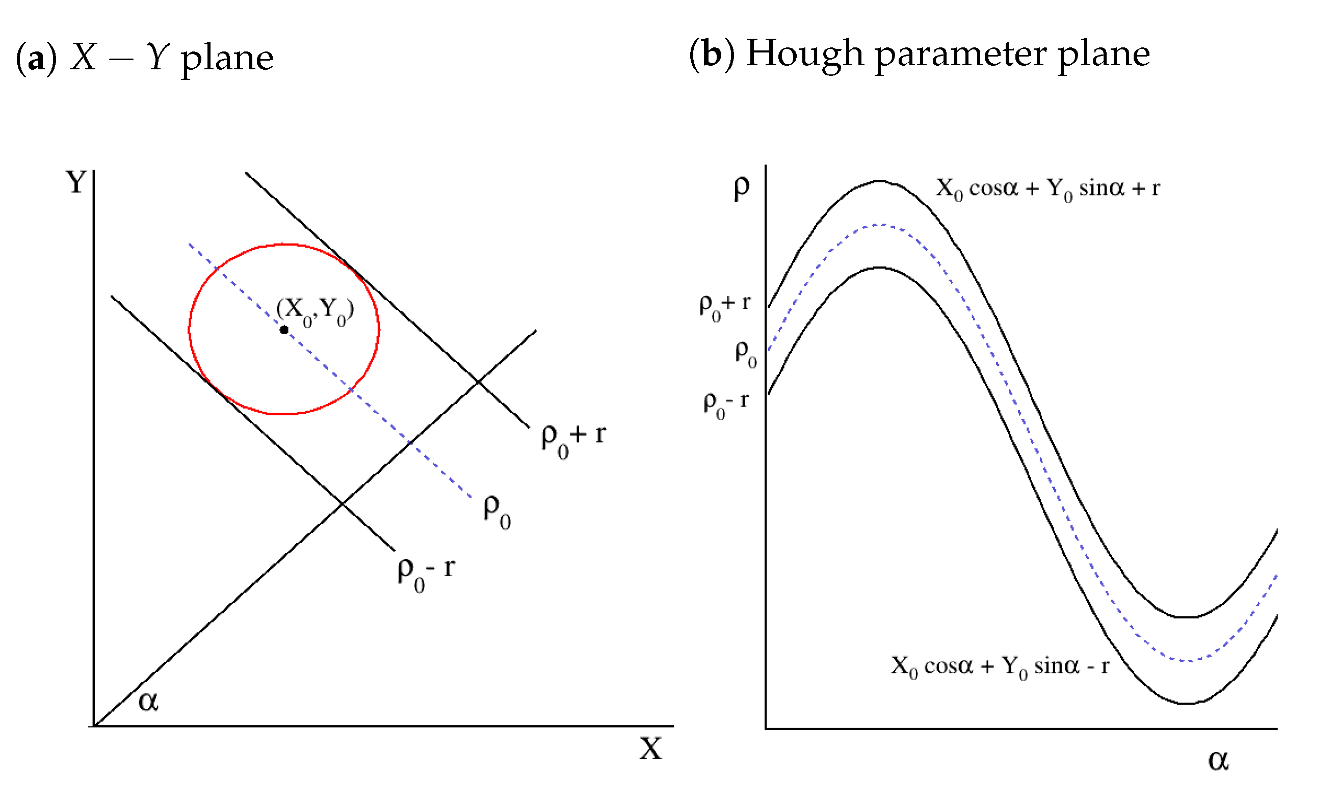
  82. Zhang, J.; Zhang, Y.; Liu, H.M.; Yuan, Y.; Zhang, X.Y.; Dong, L.Y.; Huang, Z.; Ji, X.B.; Li, H.B.; Li, W.G.; et al. Low transverse momentum track reconstruction based on the Hough transform for the BESIII drift chamber. Radiat. Detect. Technol. Methods 2018, 2, 20. [Google Scholar] [CrossRef]
  83. Sun, X.H.; Wang, L.L.; Wu, L.H.; Ju, X.D.; Xiu, Q.L.; Dong, L.Y.; Dong, M.Y.; Li, W.D.; Liu, H.M.; Liu, H.M. Track segment finding with CGEM-IT and matching to outer drift chamber tracks in the BESIII detector. Chin. Phys. C 2016, 40, 096203. [Google Scholar] [CrossRef]
  84. Huang, Z. Global Track Finding with a Cylindrical GEM and a Drift Chamber. In Proceedings of the 24th International Conference on Computing in High-Energy and Nuclear Physics (CHEP2019), Adelaide, Australia, 4–8 November 2019; Available online: https://indico.cern.ch/event/773049/contributions/3474780/attachments/1937588/3211997/Global_Track_Finding_with_a_Cylindrical-GEM_and_a_Drift_Chamberposter.pdf (accessed on 31 January 2022).
  85. Hough, P.V.C. Method and Means for Recognizing Complex Patterns. U.S. Patent 3,069,654, 18 December 1962. [Google Scholar]
  86. SPS Website. Available online: https://sba.web.cern.ch/sba/BeamsAndAreas/H4/H4_presentation.html (accessed on 31 January 2022).
  87. Collaboration RD51 Website. Available online: https://rd51-public.web.cern.ch/ (accessed on 31 January 2022).
  88. Dalla Torre, S.; Oliveri, E.; Ropelewski, L.; Titov, M. R&D proposal RD51 extension beyond 2018. arXiv 2018, arXiv:1806.09955. [Google Scholar]
  89. Rosenthal, M.; Charitonidis, N.; Chatzidaki, P.; Margraf, R.; Wilkens, H.; Bergsma, F.; Pierre-Ange, G. Magnetic Field Measurements of the GOLIATH Magnet in EHN1. 2018. Available online: http://cds.cern.ch/record/2310483/files/CERN-ACC-NOTE-2018-0028.pdf (accessed on 31 January 2022).
  90. Farinelli, R.; Amoroso, A.; Baldini Ferroli, R.; Balossino, I.; Bertani, M.; Bettoni, D.; Bortone, A.; Calcaterra, A.; Cerioni, S.; Cheng, W.; et al. Preliminary results from the cosmic data taking of the BESIII cylindrical GEM detectors. In Proceedings of the International Conference on Instrumentation for Colliding Beam Physics (INSTR2020), Novosibirsk, Russia, 24–28 February 2020. [Google Scholar]
  91. Farinelli, R.; Alexeev, M.; Amoroso, A.; Bagnasco, S.; Baldini Ferroli, R.; Balossino, I.; Bertani, M.; Bettoni, D.; Bortone, A.; Bianchi, F.; et al. GRAAL: Gem Reconstruction and Analysis Library. In Proceedings of the International Workshop on Advanced Computing and Analysis Techniques in Physics Research (ACAT2019), Saas-Fee, Switzerland, 11–15 March 2019. [Google Scholar]
  92. Garzia, I.; Alexeev, A.A.; Baldini Ferroli, R.; Balossino, I.; Bertani, M.; Bettoni, D.; Bortone, A.; Calcaterra, A.; Cerioni, S.; Capodiferro, M.; et al. GEM detector performance with innovative micro-TPC readout in high magnetic field. In Proceedings of the Advancements in Nuclear Instrumentation Measurement Methods and Their Applications (ANIMMA 2017), Liege, Belgium, 19–23 June 2017; p. 170. [Google Scholar]
  93. Farinelli, R.; Amoroso, A.; Baldini Ferroli, R.; Balossino, I.; Bertani, M.; Bettoni, D.; Bortone, A.; Calcaterra, A.; Cerioni, S.; Cheng, W.; et al. A Cylindrical GEM Inner Tracker for the BESIII Experiment At IHEP. In Proceedings of the International Conference on Technology and Instrumentation in Particle Physics (TIPP2017), Beijing, China, 22–26 May 2017; Springer: Singapore, 2018; Volume 213, pp. 116–119. [Google Scholar]
  94. National Instruments Corp. LabVIEW Documentation. Available online: https://www.ni.com/it-it/support/documentation.html (accessed on 31 January 2022).
  95. Arduino Documentation. Available online: https://docs.arduino.cc/ (accessed on 31 January 2022).
  96. InfluxData Inc. InfluxDB Documentation. Available online: https://docs.influxdata.com/influxdb/v2.1/ (accessed on 31 January 2022).
  97. Grafana Labs. Grafana Documentation. Available online: https://grafana.com/docs/grafana/latest/ (accessed on 31 January 2022).
Figure 1. BESIII spectrometer layout: the beam pipe is at the bottom of the picture where the red diamond identifies the interaction point. Each detection system is highlighted in a different color. The full detector has a cylindrical symmetry around the beam pipe, a radius of 2.5 m, and a length of 5.6 m.
Symmetry 14 00905 g001
Figure 2. Relative gain with respect to the value in 2009 (at commissioning time) as a function of the layer number in the MDC. The IDC comprises the first eight layers, and the ODC the others [21].
Symmetry 14 00905 g002
Figure 3. Design of the CGEM-IT for BESIII. 3D representation of the inner, middle, and outer triple-GEM layers with their mechanical supports. Some readout and high voltage boards are shown on the outer layer as an example [23].
Symmetry 14 00905 g003
Figure 4. Illustrations of a GEM-based detector. (a) Single GEM detector scheme. Reprinted with permission from Reference [26]. (b) Field lines inside the GEM holes [27].
Symmetry 14 00905 g004
Figure 5. Effective gain (solid lines) and discharge probability (dashed lines) with respect to voltage applied in single, double, or triple−GEM configurations [27].
Symmetry 14 00905 g005
Figure 6. Schematic representation of cylindrical triple−GEM structure. (a) Layout of a single layer; (b) sketch of the strip orientation on the cylinder.
Symmetry 14 00905 g006
Figure 7. Detail of the mechanical structure at one extremity of the CGEM−IT for BESIII. Arrows indicate relevant details [36].
Symmetry 14 00905 g007
Figure 8. Details of the validation and construction processes. (a) Test of the vacuum system. Here the weak spots are reported (protrusion and overlap); (b) HV test box with a GEM foil ready to be tested; (c) Schematic representation of the machine for the resizing of the GEM foil; (d) VIM during operation. Reprinted with permission from Reference [26].
Symmetry 14 00905 g008
Figure 9. Drawing of the mold used for the sub−layer. Arrows indicate some details that are useful during the construction. Reprinted with permission from Reference [26].
Symmetry 14 00905 g009
Figure 10. Drawing of the preparation of a sub−layer. From left to right, top to bottom: inner−ring placed on the mold; wrapping of the GEM foil; installation of the outer−ring; final gluing; sub−layer ready. Reprinted with permission from Reference [26].
Symmetry 14 00905 g010
Figure 11. Photos of the investigation tests on the innermost layer of the first production. (a) Laser measurement; (b) CT scan measurement [38].
Symmetry 14 00905 g011
Figure 12. Overview of the CGEM−IT electronics readout chain, from the detector to the BESIII Data Acquisition System [21].
Symmetry 14 00905 g012
Figure 13. Front−end board for the CGEM−IT inner layer: (a) top−side routing on FE1 and (b) FE1−FE2 assembly with copper heat−sink [23].
Symmetry 14 00905 g013
Figure 14. TIGER channel architecture scheme [23].
Symmetry 14 00905 g014
Figure 15. Time measurement concept: the coarse time information of the event triggered by the discriminator is measured with a clock counter; the fine time information, provided by the TDCs and corresponding to the time elapsing between the asynchronous trigger signal and the next clock rising edge, improves the system time resolution [23].
Symmetry 14 00905 g015
Figure 16. Comparison of the two modes for charge measurement provided by TIGER: (a) using the Sample−and−Hold circuit and (b) from Time−over−Threshold information.
Symmetry 14 00905 g016
Figure 17. Overview of a GEMROC module: (a) block diagram of the GEMROC hardware [23] and (b) schematic view of the functionalities implemented in the FPGA firmware [21].
Symmetry 14 00905 g017
Figure 18. Sketch of the simplified digitization projection of the track segment inside the drift gap onto the anode strips. Reprinted with permission from Reference [70].
Symmetry 14 00905 g018
Figure 19. Comparison between the simulated (blue triangles) and experimental (red squares) data for the four sentinel variables as a function of the incident angle, without magnetic field. Each panel shows one sentinel variable: (a) cluster size, (b) cluster charge, (c) CC resolution, (d) µTPC resolution. The experimental data analysis are addressed in Section 6 and can be found in [33,75,80].
Symmetry 14 00905 g019
Figure 20. Sketch of the position reconstruction algorithms. The five sub−layers of the triple−GEM are shown, and the orange triangular shape crossing the gaps is the electron avalanche corresponding to each ionization point (red star). The charge distribution shape on the segmented anode is the profile of the orange bars on the strips (red dashes). (a) Charge centroid method. (b) µTPC method with the straight line parametrization describing the track direction [23].
Symmetry 14 00905 g020
Figure 21. Projection of the helix trajectory onto the transverse plane. (a) Track of a negative particle. (b) Track of a positive particle. The point belonging to the track is ( x , y , z ) , while the pivot is ( x 0 , y 0 , z 0 ) . The two vectors v and w define the position of the point on the track and of the pivot with respect to the center of the helix. Reprinted with permission from Reference [81].
Symmetry 14 00905 g021
Figure 22. Track Segment Finder efficiency as a function of the transverse momentum. Reprinted with permission from Reference [83].
Symmetry 14 00905 g022
Figure 23. Drift circle in the different parameter spaces. (a) Drift circle transformed into another circle in the conformal plane ( X Y plane). (b) Drift circle transformed into two sinusoidal curves in the Hough plane, via the Legendre Transformation.
Symmetry 14 00905 g023
Figure 24. Resolution as a function of the muon momentum of the helix parameters, obtained with the full simulation of single µ events in the CGEM−IT (blue stars) and IDC (black triangles): (a) d ρ parameter; (b) d z parameter; (c) reconstructed momentum. Reprinted with permission from Reference [70].
Symmetry 14 00905 g024
Figure 25. Residual distribution (MC-reconstructed) of the J / ψ vertex position. (a) Residual in x y . (b) Residual on the z coordinate [33].
Symmetry 14 00905 g025
Figure 26. Sketch of the testbeam setup at SPS−H4 line. The detectors under test and the tracking system are placed in the middle, along the beam line, the trigger in the regions upstream, and downstream with respect to the detectors. The red cylinders represent the dipole magnets [33].
Symmetry 14 00905 g026
Figure 27. Cluster size and cluster charge measurements of a planar triple−GEM with Ar:CO 2 (70:30) and Ar:iC 4 H 10 (90:10) gas mixtures. No magnetic field is present. (a) Cluster size and cluster charge as a function of the effective detector gain. (b) Cluster size and cluster charge as a function of the incident angle; the orthogonal tracks are set to 0 [33].
Symmetry 14 00905 g027
Figure 28. Efficiency and spatial resolution of a planar triple−GEM with Ar:CO 2 (70:30) and Ar:iC 4 H 10 (90:10) gas mixtures. (a) CC resolution and efficiency as a function of the gain without magnetic field [80]. (b) CC, µTPC and merge spatial resolutions with Ar:iC 4 H 10 (90:10) gas mixture as a function of the incident angle. A magnetic field of 1 T is present, orthogonal tracks are set to 0 [33].
Symmetry 14 00905 g028
Figure 29. Testbeam results from a planar triple−GEM setup and TIGER electronics. The gas mixture is Ar:iC 4 H 10 (90:10), no magnetic field is present. (a) Cluster charge as a function of the HV applied on each GEM foil for a 0 and 45 beam incident angle [23]. (b) CC resolution as a function of the mean cluster charge for orthogonal tracks [33].
Symmetry 14 00905 g029
Figure 30. Picture of the CGEM−IT setup used for the cosmic ray data taking. The inner layer is inserted inside the middle layer. The trigger system is given by the black scintillator bars above and below it [23].
Symmetry 14 00905 g030
Figure 31. Schematic view of the acquisition and test control software tools [21].
Symmetry 14 00905 g031
Figure 32. Typical time and charge distributions produced by the online analysis of a cosmic run for the V strips of the CGEM−IT middle layer. (a) Charge versus arrival time with respect to the trigger time: the detector signal time window corresponds to the high charge time region (between −8900 ns and −8600 ns), while the low charge flat distribution is due to noise. (b) Strip charge distribution selecting only data inside the signal time window: the charge is mainly distributed on the longest strips (400−700 and 1500−1800) [21].
Symmetry 14 00905 g032
Figure 33. Preliminary results from the CGEM−IT cosmic setup with two final layers at IHEP. (a) Measured noise as a function of the V strip length for the CGEM−IT inner layer; longer strips have a larger capacitance and thus a higher noise [21]. (b) CC resolution of the CGEM−IT inner layer as a function of the track incident angle; the tracking system contribution is not subtracted [90].
Symmetry 14 00905 g033
Table 1. Main geometry characteristics for each layer.
LayerInner DiameterActive Area LengthStrips Stereo Angle
Inner153.8 mm532 mm46.7
Middle242.8 mm690 mm−31.0
Outer323.8 mm847 mm32.9
Table 2. BESIII CGEM−IT requirements [35].
CharacteristicGoal
Angular Coverage 93 % × 4 π
Material Budget≤1.5% X 0
Rate Capability 10 4 Hz / cm 2
σ r ϕ ≤130 µm
σ z ≤1 mm
dp/p @ 1GeV/c 0.5 %
Table 3. TIGER ASIC specifications.
ParametersValue
Number of channels64
Clock frequency160–200 MHz
Input capacitanceUp to 100 pF
Input dynamic range2–50 fC
Front-end gain12 mV/fC
Non-linearity<2%
ENC<2000 e
TDC time binning50 ps
Maximum event rate60 kHz/ch
Readout modeTrigger-less
Charge collectiontTime60 ns
Time resolution<5 ns
Power consumption<12 mW/ch
TechnologyCMOS 110 nm
Publisher’s Note: MDPI stays neutral with regard to jurisdictional claims in published maps and institutional affiliations.

