

New Formulation to Synthetize Semiconductor Bi2S3 Thin Films Using Chemical Bath Deposition for Optoelectronic Applications

 , ,
, , 
Abstract
1. Introduction
2. Materials and Methods
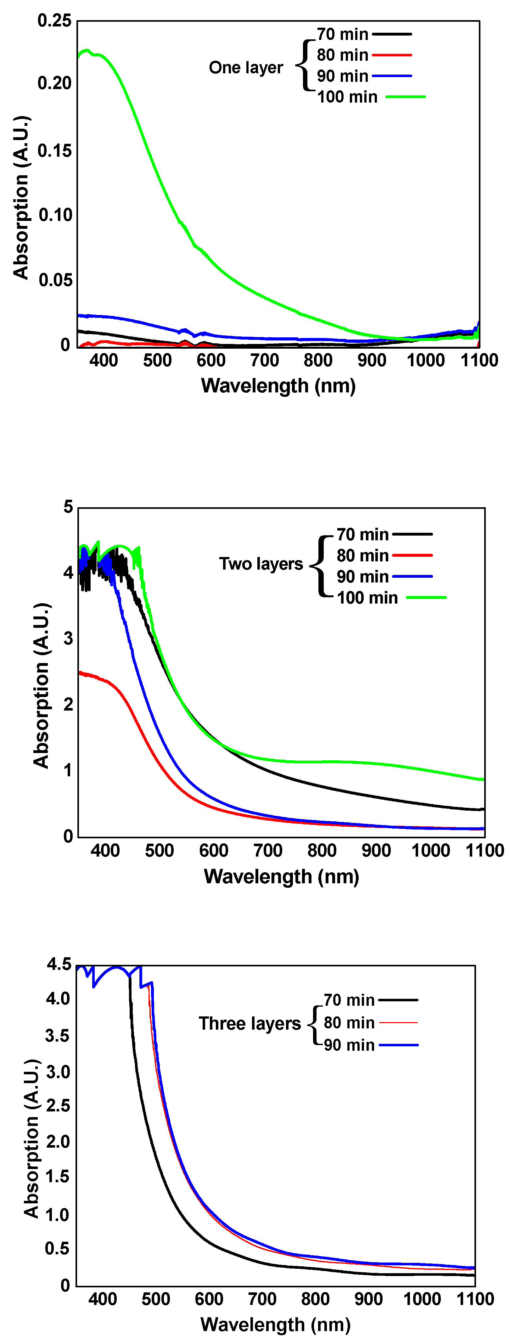
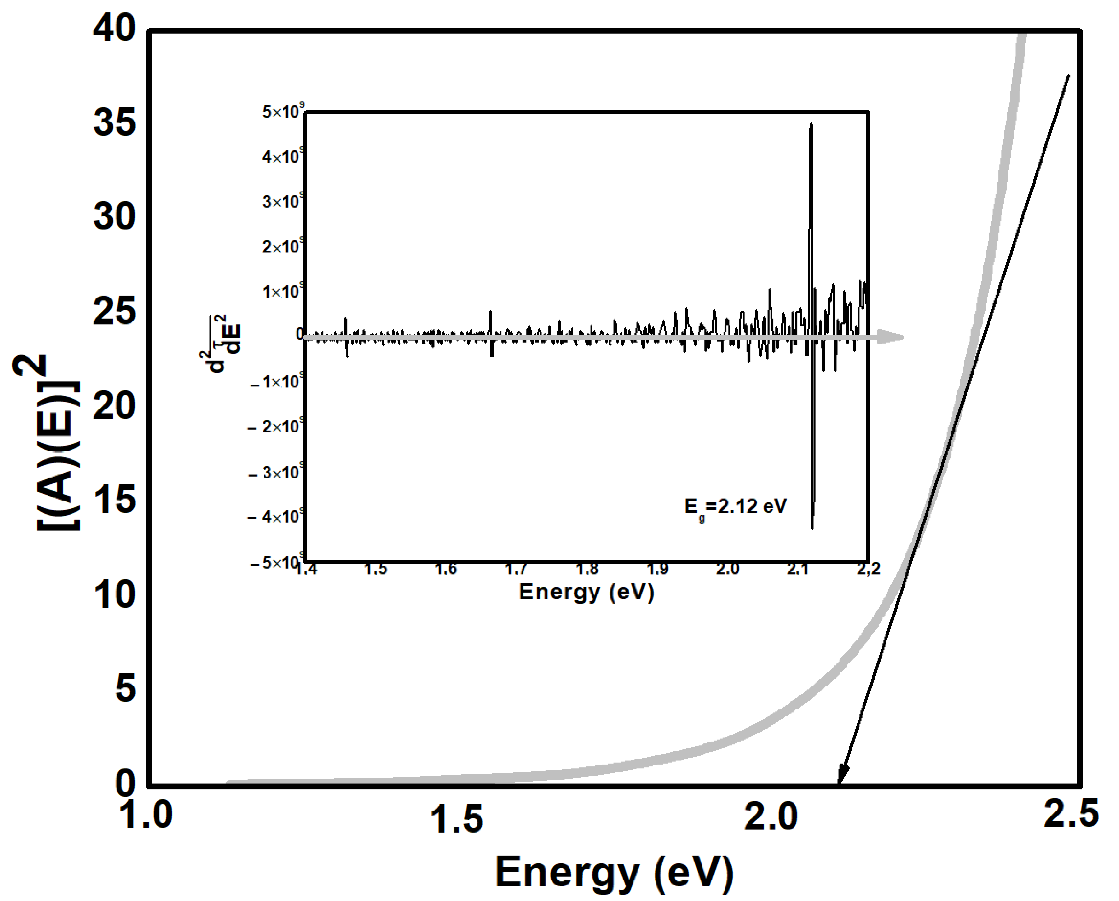
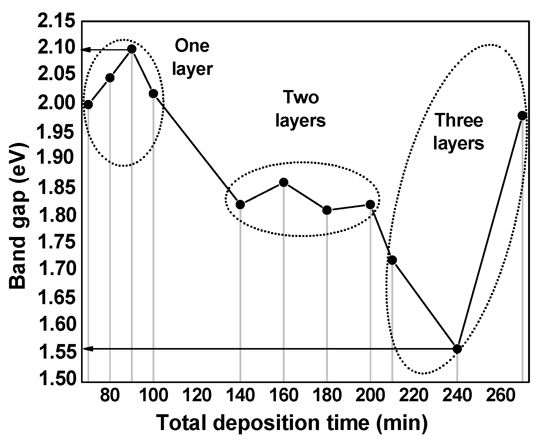
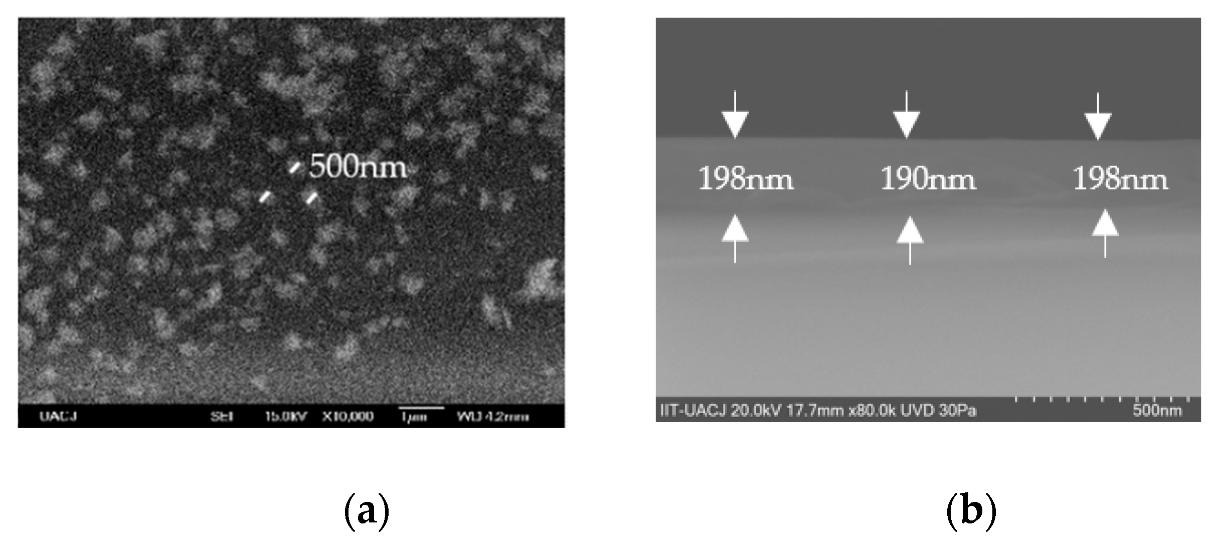
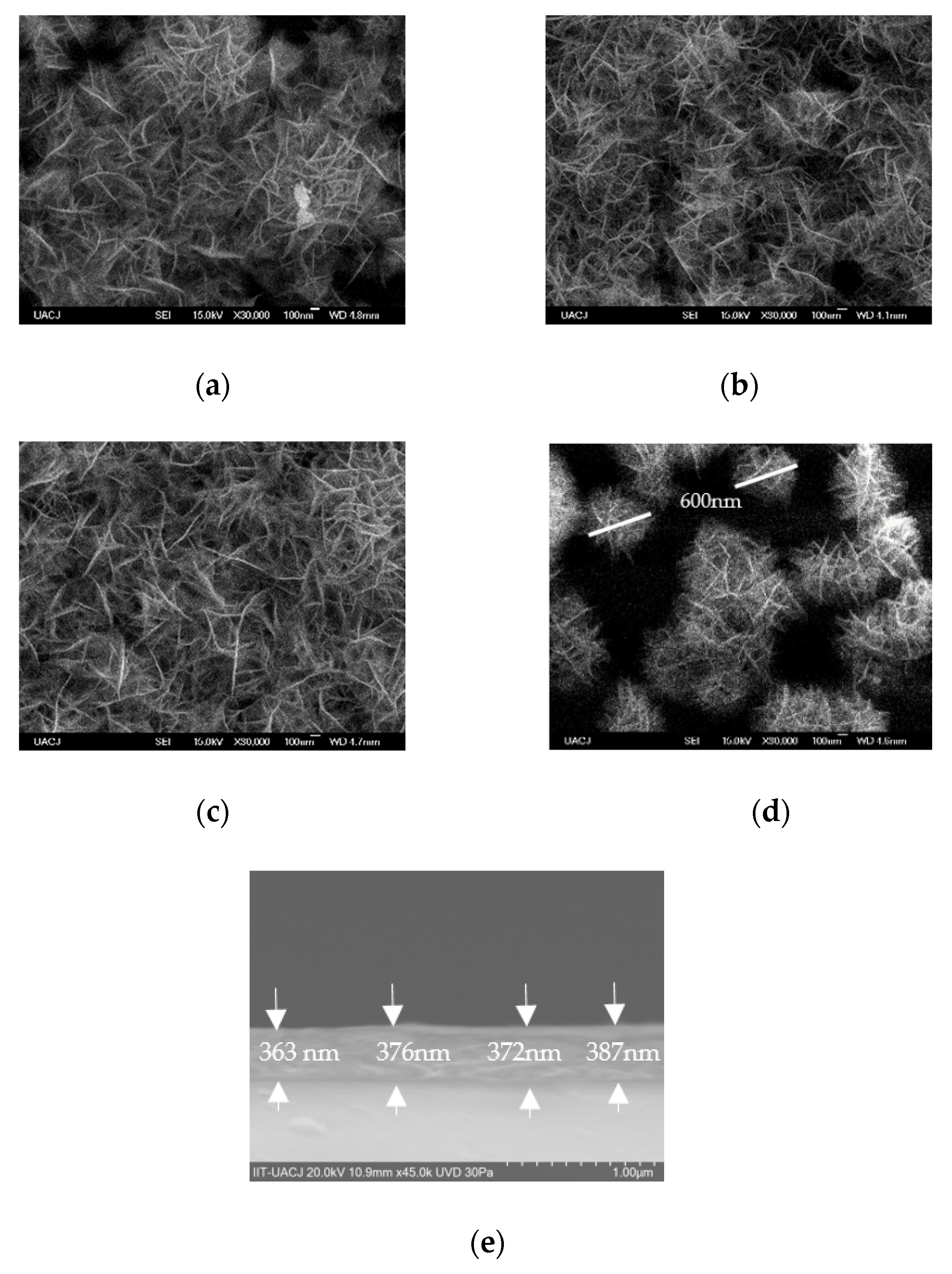
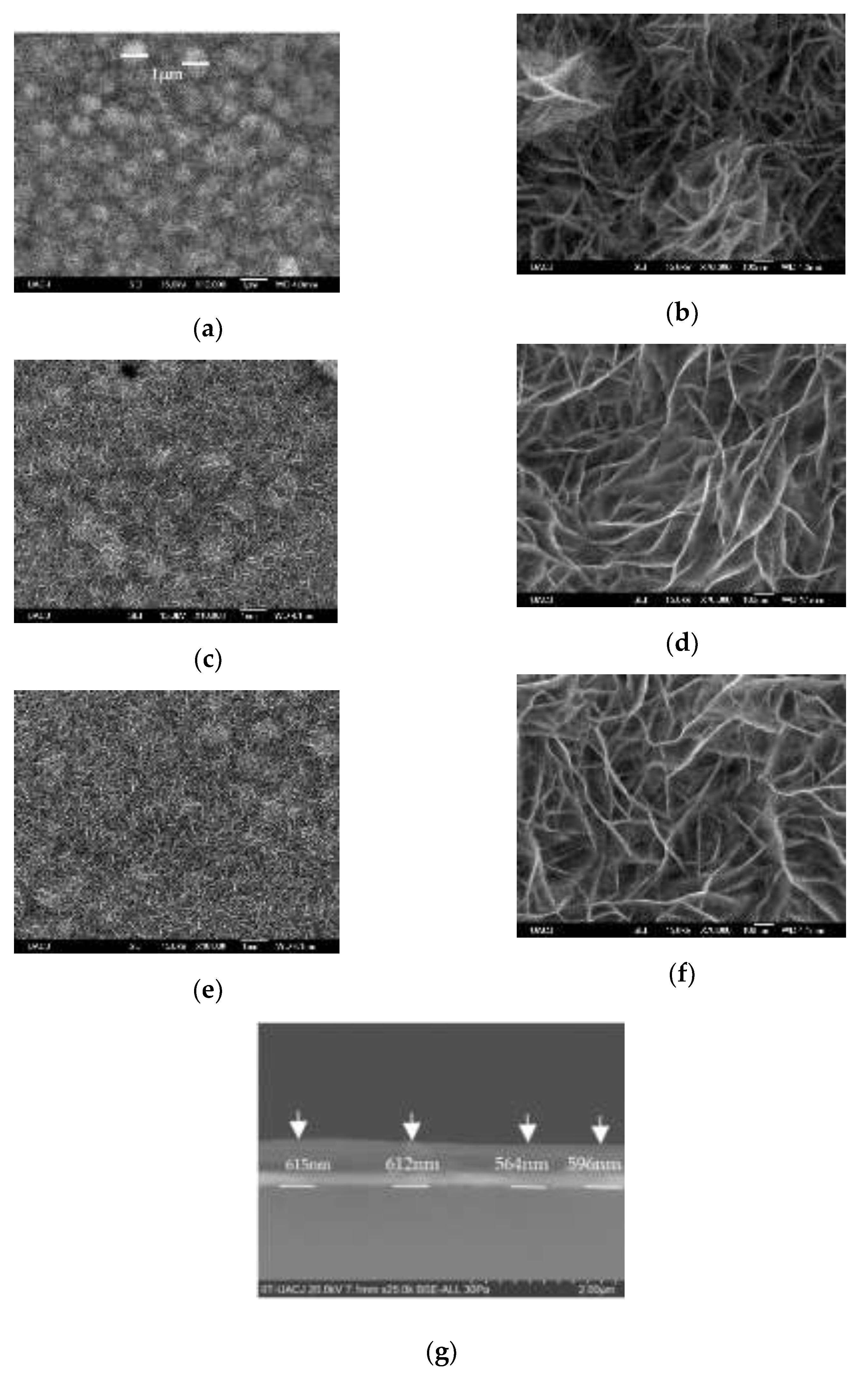
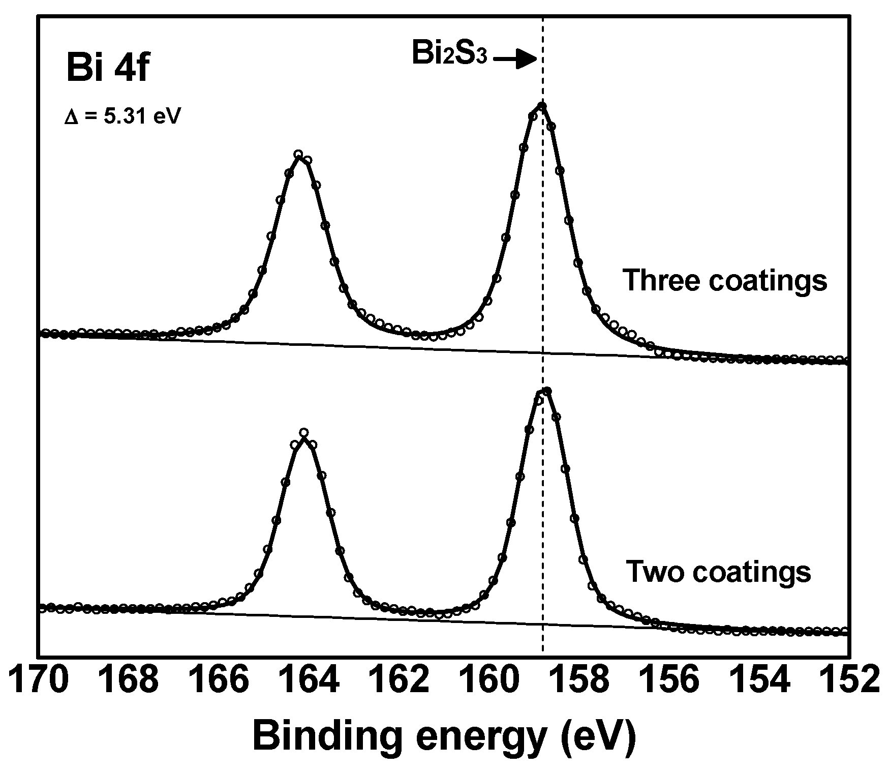
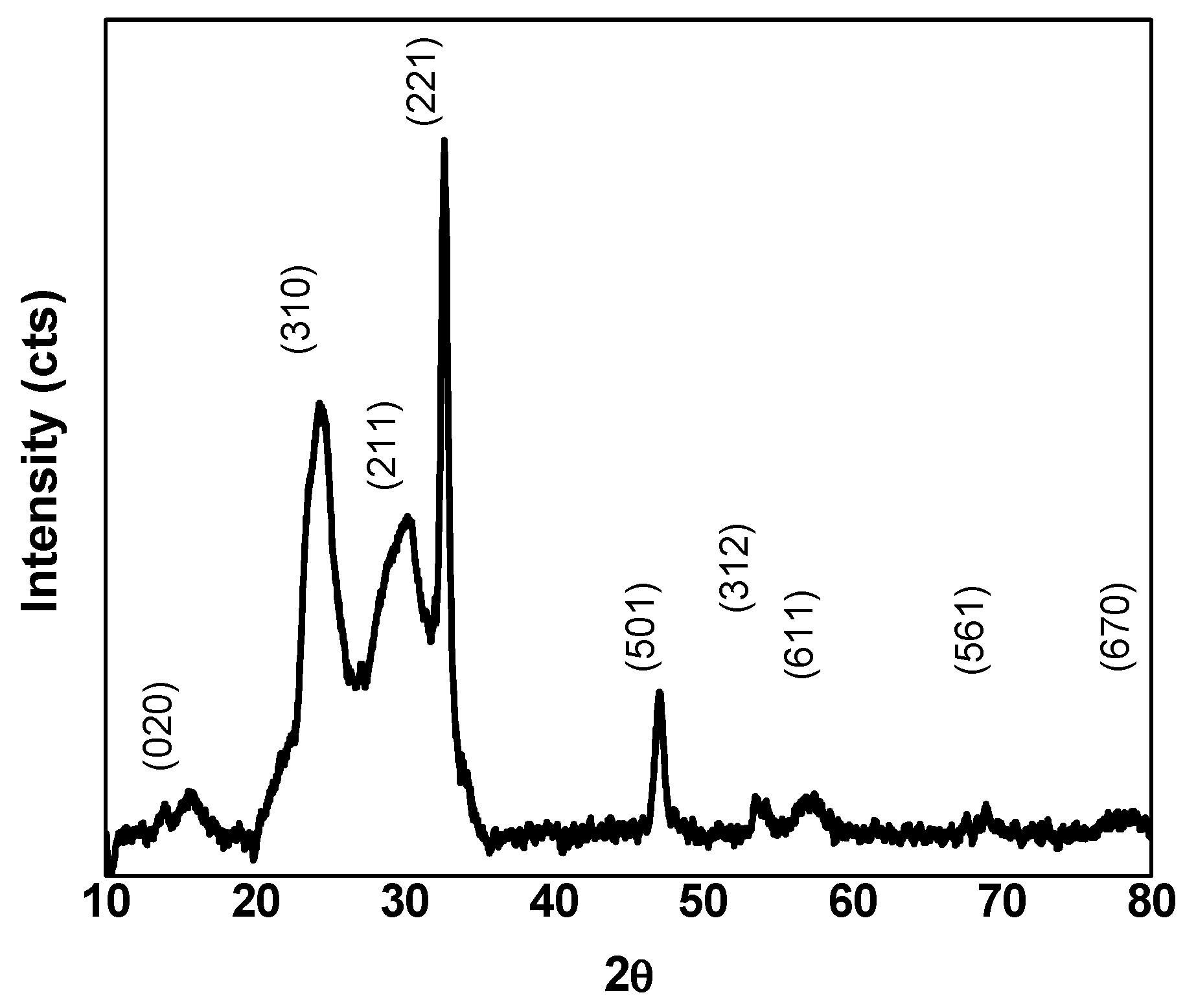
3. Results and Discussion
4. Conclusions
Author Contributions
Funding
Data Availability Statement
Acknowledgments
Conflicts of Interest
References
- García, M.H.; Nair, M.T.S.; Nair, P.K. All-chemically deposited Bi2S3/PbS solar cells. Thin Solid Films 2011, 519, 7364–7368. [Google Scholar] [CrossRef]
- Liufu, S.C.; Chen, L.D.; Yao, Q.; Wang, C.F. Bismuth Sulfide Thin Films with Low Resistivity on Self-Assembled Monolayers. J. Phys. Chem. B 2006, 47, 24054–24061. [Google Scholar] [CrossRef] [PubMed]
- Nair, P.K.; Nair, M.T.S.; Garcia, V.M.; García, O.L.; Arenas, O.L.; Piña, Y.; Castillo, A.; Ayala, I.T.; Gomezdaza, O.; Sánchez, A.; et al. Semiconductor thin films by chemical bath deposition for solar energy related applications. Sol. Energy Mater. Sol. Cells 1998, 52, 313–344. [Google Scholar] [CrossRef]
- Nie, G.; Lu, X.; Lei, J.; Yang, L.; Wang, C. Facile and controlled synthesis of bismuth sulfide nanorods-reduced graphene oxide composites with enhanced supercapacitor performance. Electrochim. Acta. 2015, 154, 24–30. [Google Scholar] [CrossRef]
- Miller, N.C.; Bernechea, M. Research Update: Bismuth based materials for photovoltaics. Appl. Mater. 2018, 6, 084503. [Google Scholar]
- Herner, S.B. Chapter 13—Application of Thin Films in Semiconductor Memories. In Handbook of Thin Film Deposition, 4th ed.; Elsevier: Amsterdam, The Netherlands, 2018; pp. 417–437. [Google Scholar]
- Zhu, Q.; Gao, F.; Yang, Y.; Zhang, B.; Wang, W. Electrochemical preparation of polyaniline capped Bi2S3 nanocomposite and its application in impedimetric DNA biosensor. Sens. Actuators B. Chem. 2015, 207, 819–826. [Google Scholar] [CrossRef]
- Fernandes, A.M.; Abdalhai, M.H.; Ji, J.; Xi, B.W.; Xie, J.; Sun, J.; Noeline, R.; Lee, B.H.; Sun, X. Development of highly sensitive electrochemical genosensor based on multiwalled carbon nanotubes-chitosan-bismuth and lead sulfide nanoparticles for the detection of pathogenic Aeromonas. Biosens. Bioelectron. 2015, 63, 399–406. [Google Scholar] [CrossRef]
- Kinsella, M.; Jimenez, R.E.; Karmali, P.P.; Rush, A.M.; Kotamraju, V.R.; Gianneschi, N.C.; Ruoslathi, E.; Stupack, D.; Sailor, M.J. X-ray computed tomography imaging of breast cancer by using targeted peptide-labeled bismuth sulfide nanoparticles. Angew. Chem. Int. Ed. 2011, 50, 12308–12311. [Google Scholar] [CrossRef]
- Qu, C.; Zhou, S.; Li, G.; Wang, C.; Synders, R.; Bittencourt, C.; Li, W. Bi2S3/rGO Composite Based Electrochemical Sensor for. Ascorbic Acid Detection. Chemosensors 2021, 9, 190–205. [Google Scholar] [CrossRef]
- Gao, C.; Shen, H.; Sun, L.; Shen, Z. Chemical bath deposition o Bi2S3 films by a novel deposition system. Appl. Surf. Sci. 2011, 257, 7529–7533. [Google Scholar] [CrossRef]
- Ali, N.; Hussain, A.; Ahmed, R.; Omar, M.F.B.; Sultan, M.; Fu, Y.Q. Crystallized InBiS3 thin films with enhanced optoelectronic properties. Appl. Surf. Sci. 2018, 436, 293–301. [Google Scholar] [CrossRef]
- Munawar, K.; Mansoor, M.A.; Basirun, W.J.; Misran, M.; Huang, N.M.; Mazhar, M. Single step fabrication of CuO-MnO-2TiO2 composite thin films with improved photoelectrochemical response. RSC Adv. 2017, 7, 15885–15893. [Google Scholar] [CrossRef]
- Zamani, M.; Jamali-Sheini, F.; Cheraghizade, M. Visible-range and self-powered bilayer p-Si/n-Bi2S3 heterojunction photodetector: The effect of Au buffer layer on the optoelectronics performance. J. Alloy. Compd. 2022, 905, 164119–164149. [Google Scholar] [CrossRef]
- Ho, S.M.; Nilai, P.; Sembilan, N. Review Article Chalcogenide Thin Films Prepared using Chemical Bath Deposition Method: Review. Res. J. Appl. Sci. Eng. Technol. 2015, 11, 1058–1065. [Google Scholar] [CrossRef]
- Pineda, E.; Nicho, M.E.; Nair, P.K.; Hu, H. Optoelectronic properties of chemically deposited Bi2S3 thin films and the photovoltaic performance of Bi2S3/P3OT solar cells. Sol. Energy 2012, 86, 1017–1022. [Google Scholar] [CrossRef]
- Luo, Y.; Wen, J.; Zhang, J. Introductory Chapter: BISMUTH-Related Optoelectronic Materials. In Bismuth-Fundamentals and Optoelectronic Applications, 1st ed.; Intechopen: London, UK, 2020. [Google Scholar]
- Toudert, J.; Serna, R.; Deeb, C.; Rebollar, E. Optical properties of bismuth nanostructures towards the ultrathin film regime. Opt. Mater. Express 2019, 9, 2924–2936. [Google Scholar] [CrossRef]
- Wang, F.; Yang, S.; Wu, J.; Hu, X.; Li, Y.; Li, H.; Liu, X.; Luo, J.; Zhai, T. Emerging two-dimensional bismuth oxychalcogenides for electronics and optoelectronics. InfoMat 2021, 3, 1251–1271. [Google Scholar] [CrossRef]
- Pandey, A.; Yadav, R.; Kaur, M.; Singh, P.; Gupta, A.; Husale, S. High performing flexible optoelectronic devices using thin films of topological insulator. Sci. Rep. 2021, 11, 832. [Google Scholar] [CrossRef] [PubMed]
- Patil, A.L.; Chanshetti, U.B. Refractive Index and Density Properties of Bismuth Sulfide (Bi2S3) Glass Nanocomposite. Int. J. Mater. Sci. 2017, 12, 1–7. [Google Scholar]
- Wang, Y.; Chen, J.; Jiang, L.; Sun, K.; Liu, F.; Lai, Y. Photoelectrochemical properties of Bi2S3 thin films deposited by successive ionic layer adsorption and reaction (SILAR) method. J. Alloy. Compd. 2016, 686, 684–692. [Google Scholar] [CrossRef]
- Fazal, T.; Ismail, B.; Shah, M.; Iqbal, S.; Elkaeed, E.B.; Awwad, N.S.; Ibrahium, H.A. Simplified Route for Deposition of Binary and Ternary Bismuth Sulphide Thin Films for Solar Cell Applications. Sustainability 2022, 14, 4603–4614. [Google Scholar] [CrossRef]
- Ahire, R.R.; Sharma, R.P. Photoelectrochemical characterization of Bi2S3 thin films deposited by modified chemical bath deposition. Indian J. Eng. Mater. Sci. 2006, 13, 140–144. [Google Scholar]
- Hodes, G. Chemical Solution Deposition of Semiconductor Films, 1st ed.; Marcel Dekker: New York, NY, USA, 2002. [Google Scholar]
- Hussain, A.; Ahmed, R.; Ali, N.; AbdEl-Salam, N.M.; Deraman, K.; Fu, Y.Q. Synthesis and characterization of thermally evaporated copper bismuth sulphide thin films. Surf. Coat. Technol. 2017, 320, 404–408. [Google Scholar] [CrossRef]
- Nair, M.T.S.; Nair, P.K. Photoconductive bismuth sulphide thin films by chemical deposition. Semicond. Sci. Technol. 1990, 5, 1225. [Google Scholar] [CrossRef]
- Mane, R.S.; Sankapal, B.R.; Lokhande, C.D. Photoelectrochemical (PEC) characterization of chemically deposited Bi2S3 thin films from non-aqueous medium. Mater. Chem. Phys. 1999, 60, 158–162. [Google Scholar] [CrossRef]
- Shah, M.P.; Holmberg, S.H.; Kostylev, S.A. Reversible switching in thin amorphous chalcogenide films—Electronic effects. Phys. Rev. Lett. 1973, 31, 542. [Google Scholar] [CrossRef]
- Subramania, S.; Balaji, M.; Chithralekha, P.; Sanjeev, G.; Subramanian, E.; Pathinettam, D. Electron beam induced modifications of bismuth sulphide (Bi2S3) thin films: Structural and optical properties. Radiat. Phys. Chem. 2010, 79, 1127–1131. [Google Scholar] [CrossRef]
- Shein, H.; Shao, Z.; Zhao, Q.; Jin, M.; Shen, C.; Deng, M.; Zhong, G.; Huang, F.; Zhu, H.; Chen, F.; et al. Facile synthesis of novel three-dimensional Bi2S3 nanocrystals capped by polyvinyl pyrrolidone to enhance photocatalytic properties under visible light. J. Colloid Interface Sci. 2020, 573, 115–122. [Google Scholar] [CrossRef]
- Onwudiwe, D.C.; Nkwe, V.M. Morphological variations in Bi2S3 nanoparticles synthesized by using a single source precursor. Heliyon 2020, 7, e04505. [Google Scholar] [CrossRef]
- Liu, K.; Shen, Z.R.; Li, Y.; Han, S.D.; Hu, T.L.; Zhang, D.S.; Bu, X.H.; Ruan, W.J. Solvent induced rapid modulation of micro/nano structures of metal carboxylates coordination polymers: Mechanism and morphology dependent magnetism. Sci. Rep. 2014, 4, 6023–6029. [Google Scholar] [CrossRef]
- Yu, I.; Isobe, T.; Seena, M. Preparation and properties of CdS thin films comprising nano-particles by a solution growth technique. Mater. Res. Bull. 1995, 30, 975–980. [Google Scholar] [CrossRef]
- Wagner, C.D.; Naumkin, A.V.; Kraut-Vass, A.; Allison, J.W.; Powell, C.J.; Rumble, J.R. NIST Standard Reference Database 20; Version 3.4; Available online: http:/srdata.nist.gov/xps/ (accessed on 10 December 2021).
- Ahire, R.R.; Sankapal, B.R.; Lokhande, C.D. Preparation and characterization of Bi2S3 thin films using modified chemical bath deposition method. Mater. Res. Bull. 2001, 36, 199–210. [Google Scholar] [CrossRef]
- Hussain, A.; Begum, A.; Rahman, A. Effects of annealing on nanocrystalline Bi2S3 thin films prepared by chemical bath deposition. Mater. Sci. Semicond. Process. 2014, 2, 74–81. [Google Scholar] [CrossRef]
- Moreno-García, H.; Messina, S.; Calixto-Rodriguez, M.; Martínez, H. Physical properties of chemically deposited Bi2S3 thin films using two post-deposition treatments. Appl. Surf. Sci. 2014, 311, 729–733. [Google Scholar] [CrossRef]


| Sm,n~Total Deposition Time (Minutes) | m, Represents the Number of Layers | ||
|---|---|---|---|
| n, represents the deposition time | S1,70~70 | S2,70~140 | S3,70~210 |
| S1,80~80 | S2,80~160 | S3,80~240 | |
| S1,90~90 | S2,90~180 | S3,90~270 | |
| S1,100~100 | S2,100~200 | S3,100~300 | |
Publisher’s Note: MDPI stays neutral with regard to jurisdictional claims in published maps and institutional affiliations. |
© 2022 by the authors. Licensee MDPI, Basel, Switzerland. This article is an open access article distributed under the terms and conditions of the Creative Commons Attribution (CC BY) license (https://creativecommons.org/licenses/by/4.0/).
Share and Cite
Carrillo-Castillo, A.; Rivas-Valles, B.G.; Castillo, S.J.; Ramirez, M.M.; Luque-Morales, P.A. New Formulation to Synthetize Semiconductor Bi2S3 Thin Films Using Chemical Bath Deposition for Optoelectronic Applications. Symmetry 2022, 14, 2487. https://doi.org/10.3390/sym14122487
Carrillo-Castillo A, Rivas-Valles BG, Castillo SJ, Ramirez MM, Luque-Morales PA. New Formulation to Synthetize Semiconductor Bi2S3 Thin Films Using Chemical Bath Deposition for Optoelectronic Applications. Symmetry. 2022; 14(12):2487. https://doi.org/10.3390/sym14122487
Chicago/Turabian StyleCarrillo-Castillo, Amanda, Brayan G. Rivas-Valles, Santos Jesus Castillo, Marcela Mireles Ramirez, and Priscy Alfredo Luque-Morales. 2022. "New Formulation to Synthetize Semiconductor Bi2S3 Thin Films Using Chemical Bath Deposition for Optoelectronic Applications" Symmetry 14, no. 12: 2487. https://doi.org/10.3390/sym14122487
APA StyleCarrillo-Castillo, A., Rivas-Valles, B. G., Castillo, S. J., Ramirez, M. M., & Luque-Morales, P. A. (2022). New Formulation to Synthetize Semiconductor Bi2S3 Thin Films Using Chemical Bath Deposition for Optoelectronic Applications. Symmetry, 14(12), 2487. https://doi.org/10.3390/sym14122487