Abstract
This paper reports the generation of an extra phase and the accompanying temporal effects in an asymmetric optically compensated in-pane-switching (IPS) liquid crystal (LC) system and a fringe-field-switching (FFS) liquid crystal display (LCD) exhibiting a twofold faster response speed in the switching-off process compared with that in single and symmetric IPS-LCDs and FFS LCDs for the first time. To explain the experimental results, we derived an approximate analytical formula for the optical output intensity that includes an extra phase advancement and conducted simulations to achieve normally black operation using a dynamic optical retarder.
1. Introduction
Liquid crystal displays (LCDs) are widely used as information displays for televisions, computer monitors, and various instruments. Among the various LCD operation modes, in-plane-switching (IPS) [1] and fringe-field-switching (FFS) [2] are currently widely used because of the excellent wide viewing angles of IPS and FFS displays. However, their response speed needs further improvement. To solve this problem, several methods have been adopted (1) using liquid crystal (LC) materials with low viscosity [3,4], (2) devising electrode structures [5,6], (3) doping with chiral agents [7], (4) doping with nanoparticles [7], (5) using ferroelectric LC materials [8,9], (6) using an LCD with a narrow gap cell [10], and (7) overdriving to enhance the response speed in the switching-on process [11].
Our approach reported in the present paper represents an alternative to the above-mentioned approaches. In a preliminary previous work, we reported the electro-optical performances of asymmetric optically compensated tunable birefringent (TB) mode LCD exhibiting two-fold fast response speed in the switching off process [7]. For this reason, this present work was conducted aiming at the extension of the previous work to this proposed asymmetric optically compensated IPS and FFS LCDs (Asymmetric OC-IPS and FFS-LCD). The present work is related to the geometry phase, originally described by Pancharatnum [12] and Berry [13] in their historically representative papers. The present paper also updates previous work by introducing a dynamic optical retarder [7] for realizing electro-optical characteristics with by introducing a dynamic retarder, we realized normally black state normally black operation, accompanying with a simulation utilizing a simulator, SHINTECH LCD MASTER. In conjunction with a simulation using a SHINTECH LCD MASTER simulator, we introduce a dynamic retarder, to realize normally black operation.
2. Theory
2.1. Optical Configuration of our Asymmetric IPS-LC System
In Figure 1, angle ϕ1 is the switching azimuthal angle of LC molecules and ϕ2 is the setting azimuthal angle of a compensator (+A Plate) whose angle is set to ϕ2 = 3π/4 − α, which can be controlled using a dynamic retarder, when we use an IPS cell for the compensator.
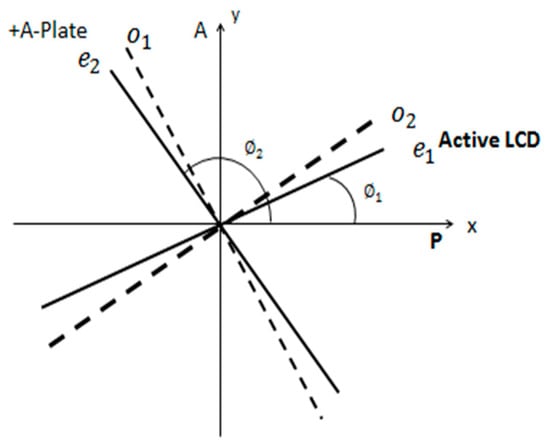
Figure 1.
Optical configuration of our asymmetric IPS-LCD (FFS-LCD) system.
The whole system is sandwiched between crossed polarizers, where the incident light field into the LCD system is polarized in the x-direction and the transmitted wave is polarized in the y-direction. Labels e1 and o1 in Figure 1 indicate that the axes of the extra-ordinary wave and the ordinary wave, respectively, and labels e2 and o2 indicate those of the compensator, respectively.
When ϕ2 = 3π/4 and ϕ1 = π/4, the system is symmetric and generates a black state; under these conditions, the extra phase is not generated and the high response speed is not achieved.
2.2. Analytical Derivation of Normalized Optical Transmission of a Single IPS-Cell
Using the system shown in Figure 1, we here carry out a 2 × 2 Jones matrix calculation [14] for I1 of a single cell.
The input electrical field is
We then have a projected field in the x-y coordinate:
where c1 and s1 are cos(ϕ1) and sin(ϕ1), respectively, here G11 = exp(−i Γ11) and G12 = exp(−i Γ12); in addition, δ1 = Γ11 − Γ12, where each of which is the phase delay in the e1 and o1, from the incident wave, respectively.
We have the x-y components such that:
E1(x) = [(c1)2 exp(−iδ1) + (s1)2]E0,
E1(y) = [s1c1(exp(−iδ1) − 1)]E0,
Then,
E1(y) = E0 sin(ϕ1)cos(ϕ1) exp(−iδ1).
= 2E0 sin(2ϕ1)exp(−iδ1).
Thus, we have the optical output intensities and the normalized optical transmission for the single cell:
I1 = I0 sin2(2ϕ1) sin2(δ1/2).
The normalized transmission is then
T1 = sin2(2ϕ1).
A δ1 = 1.3π for n-IPS and n, p-FFS and 1.04π for p-IPS were determined based on the properties of the LC materials and the LCD cell fabrication details (Section 3.3).
2.3. Derivation of Normalized Optical Transmission Intensity of OC-IPS with 2 × 2 Jones Matrix Calculations
We here derive the equation for the proposed asymmetric OC-IPS and FFS shown in Figure 1. This derivation is carried out by replacing the c1 and s1 terms in Equation (1) with c2 and s2 and Γ21 − Γ22. In addition, by inserting E1(x) and E1(y), we obtain
E1(x) = (s1)2 − (c1)2 and E1(y) = −2s1c1
We derive E2(y) as follows:
where δ2 is again the difference in phase delay between the e2 and o2 axes:
δ2 = Γ21 − Γ22.
We then have:
E2(y) = 2[s2c2(c12 − s12) − s1c1(c22 − s22)] exp(−iδ2).
And δ2 = δ1 = 1.3π for n-IPS and n, p-FFS and 1.04π for p-IPS as evaluated based on the physical properties and the LCD cell fabrication conditions described in Section 3.3. Then, with sin2(ωt) = 1/2 and without exp(−iδ2) to normalize the optical intensity and transmission.
I2 = I0 sin2(2ϕ2 − 2ϕ1) sin2(δ1/2)sin2(δ2/2)
T2 = sin2 (2ϕ2 − 2ϕ1),
If we substitute ϕ2 = π/4 − α into Equation (11), we obtain an equation with a phase-advancement shift, of 2α:
T2 = I0 cos2(2ϕ1 + 2α)
In our system, the symmetry breaking introduces a phase shift, which leads to a fast response in the switching-off process. This effect is shown later in Figure 3. When LC-cell and the A-plate are crossed, ϕ1 = ϕ2 = π/4 and δ1 = δ2 = 1.3π, the symmetric system then produces the black (dark) state and no ultrafast switching process occurs.
3. Results and Discussion
3.1. Optical Configurations and Switching of Single and OC-IPS, and OC-FFS Cells with Δε > 0 and Δε < 0
Figure 2a,b show the optical configurations and switching of single and OC-IPS and OC-FFS-LCD cells used in the present research, where p and n denote Δε > 0 and Δε < 0, respectively.
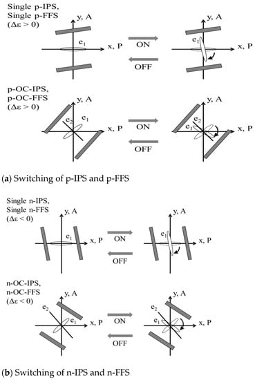
Figure 2.
Optical configuration of switching in single and optically compensated IPS- and FFS-LCDs with negative dielectric anisotropy.
We next explain the switching process in our OC-LCDs, along with the contents of Figure 2.
Figure 3 shows simulation results for the normalized transmission and compares T1 (I1) with T2 (I2) against the switching angles calculated using Equations (7) and (12). The top and central parts in this figure show the behaviors in the switching-off process, and the bottom and right parts show the behaviors in the switching-on process. Thus, the ϕ1 for T2 (I2) starts from a degree of −α, and the ϕ1 for the T1 (I1) starts from −45°.
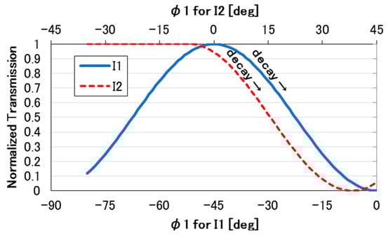
Figure 3.
Simulation results of a comparison of switching characteristics of I1 (T1) with I2 (T2) starting from the switching off process.
The results in Figure 3 are interpreted as follows (1) The T2 (I2) has a phase advancement of α over the I1(T1), (2) According to the top area, the T2 (I2) starts the decay process with a finite inclination, whereas the T1 (I1) starts the decay process with no inclination. This decay in the absence of inclination is attributed to the fast response in the decay process, which was experimentally demonstrated in the present research. This phenomenon is a purely optical effect, where the decay process occurs as the common molecular relaxation for both the symmetric and asymmetric systems. (3) The I2 (T2) has a finite value at the right bottom because of energy conservation, which means that the operation is not normally black. The realization of a normally black operation will be described in Section 3.4.
3.2. V-T Curves of Single p-IPS and p-OC-IPS Devices
Figure 4 shows the experimentally obtained transmittance-voltage (V-T)-curves of IPS LCDs, as recorded at 25 °C using a DMS-703 (Autronic Melchers, GMb) instrument. Interestingly, in the symmetric compensation system, the introduction of optical compensation introduces a wide operating voltage range, as shown in Figure 4. Regarding the V-T curve, refer to [14], where the Freedericksz transition is described.
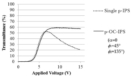
Figure 4.
Experimentally obtained V-T curves for p-IPS (Δε > 0) and p-OC-IPS devices with α = 0 (symmetric).
Figure 5 shows the V-T curves of the p-OC-IPS device without optical compensation (α = 0) and the p-OC-IPS device with optical compensation, (α = −6.8°). The proposed asymmetric OC-IP produces T = 0 at 4 V; which means a non-normally black operation. In general, an LCD is operated normally black or normally white; thus, a dynamic optical compensator, which has been updated from the device described in our previous work [7], was used (see Section 3.5).
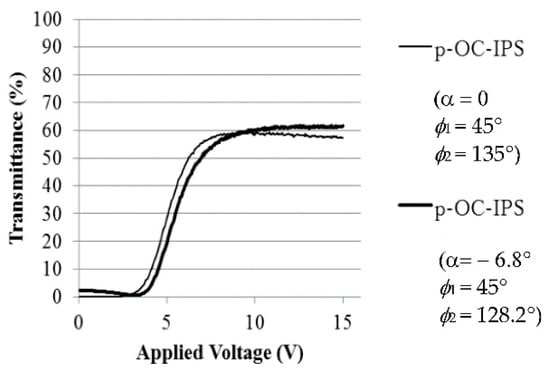
Figure 5.
Experimentally obtained V-T curves of a p-OC-IPS device without optical compensation, (α = 0) and a p-OC-PS device with optical compensation, (α = −6.8°).
3.3. Experimental Results of Response Time
The physical properties of the LC materials and the specifications of the LCD cells used in the present work are described as follows: The cell gap of the sample cells was 3.5 μm and the wavelength of the optical light source was 589 nm. The anisotropy of refractive index,
Δn (at 589 nm, 25 °C) and Δε (25 °C) (After Datasheet of DIC)
| p-IPS | 0.088 | 6.2 |
| n-IPS | 0.110 | −4.1 |
| p-FFS | 0.110 | 11.9 |
| n-FFS | 0.110 | −4.1 |
Using these quantities,
The experimental results in Table 1 and Table 2, indicate that the response time of the proposed asymmetric OC-IPS and OC-FFS devices are reduced by 42–56% compared with those of single cells and symmetric OC-IPS and OC-FFS devices. Approximately the same results were obtained for the OC-FFS device, and we will report the corresponding data elsewhere. These results indicate that the response time in the switching-on process will be greatly reduced by adopting the overdriving technique [12].

Table 1.
Results of response time for the n-OC-IPS device.
Table 2.
Results of response time for the p-OC-IPS device.
3.4. Temporal Derivatives of I1 and I2 and Their Comparison
We here derive temporal derivatives of I1 and I2
For an OC-IPS:
Thus, we obtain a formula, the F-function, by taking the ratio between Equations (13) and (14) as follows, where the two minus signs cancel each other:
The F-function () is shown in Figure 6.
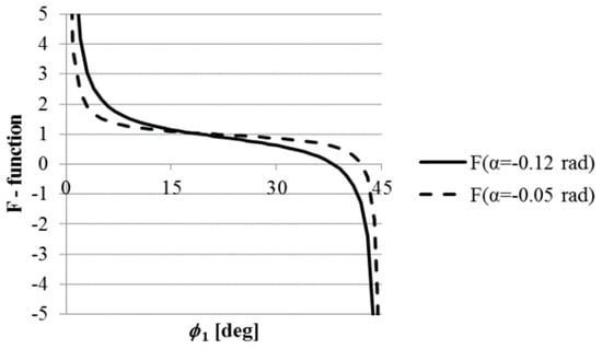
Figure 6.
The F-functions with α = −0.12 rad and α = −0.05 rad.
Figure 6 shows that the temporal derivative of I2 is much larger than that of I1 during the switching-off process, consistent with the experimental results obtained in the present work. However, it also shows that this effect terminates at a switching angle of 15° and that the relation is thereafter inverted. However, if necessary, a dynamic compensator can be used to eliminate the phase-advancement after the decay process for the switching-on process, the removal of the applied voltage causes an overvoltage, resolving this problem [11].
3.5. Dynamic Compensator
A dynamic compensator changes the azimuthal angle of the e-axis, , by applying a computer-controlled electric voltage, Vappl, according to the following equation:
α = α0 exp [1 − kVth/Vappl], k > 1 (k = 2.5)
- (1)
- For the switching-on operation (starting from Vappl ≈ 0), normally black operation will be induced with α = 0 (ϕ2 = 3π/4).
- (2)
- For the switching-off operation, where Vappl = kVth (k = 2.5), then α = α0 (~7°), extra phase, α, is generated.
This practice is demonstrated in Figure 7.
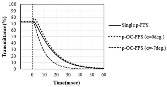
Figure 7.
Demonstration of normally black mode operation using a dynamic compensator.
4. Conclusions
- The optical output intensities were formulated using a slightly modified Jones matrix calculation, and the results showed that an extra phase accompanying temporal behavior is generated in the switching angle for the proposed asymmetric optically compensated IPS -LCD and FFS-LCD systems.
- Experiments showed that the optically compensated IPS-LCD has a broad dynamic range beyond the sine-squared oscillation in the ordinary IPS-LCD.
- Simulation results revealed the existence of phase advancement in the optical output intensity of the proposed asymmetric OC-IPS relative to that of symmetric OC-IPS, depending on the selected optical retardation in the compensator.
- Experimentally measured values of the response time of the proposed asymmetric OC-IPS-LCD and OC-FFS were reduced by 42–56% compared with those of symmetric OC-IPS, and OC-FFS, LCDs, and single IPS and FFS-LCDs.
- Temporal derivatives of the optical intensity for the proposed asymmetric OC-IPS were shown to be larger than those of the symmetric OC-IPS.
- By adopting a dynamic compensator, we demonstrated normally black operation for the proposed asymmetric OC-IPS.
Author Contributions
Conceptualization, S.K.; derivatization of analytical formulas of optical transmission, S.K.; writing, original draft preparation, S.K. and T.M.; sample fabrication and experimental measurements, H.A. and T.M.; simulations, M.K., A.I., and T.M.; All authors have read and agreed to the published version of the manuscript.
Funding
This work was partially supported by a grant from the Ministry of Education, Culture, Sports, Science and Technology, Japan (MEXT) as a project of Yamaguchi Green Materials Cluster.
Institutional Review Board Statement
Not applicable.
Informed Consent Statement
Not applicable.
Data Availability Statement
Japanese patent 6717323 (2020.7.1). Title: Method for improving response speed and liquid crystal display device, International release No.PCT/JP2016/086379. Invented by Shunsuke Kobayashi, Hidenari Akiyama, and Kenzo Takeishi.
Acknowledgments
The authors will wish to thank Haruyoshi Takatsu and Hiroshi Hasebe at DIC Corp. for their kind and enthusiastic collaboration in LC materials research. And the authors are indebted to Shoichi Ishihara at OIT for executing the preparation of this paper.
Conflicts of Interest
The authors declare no conflict of interest.
References
- Oh-e, M.; Kondo, K. Electro-optical characteristics and switching behavior of the in-plane switching mode. Appl. Phys. Lett. 1995, 67, 3895–3897. [Google Scholar] [CrossRef]
- Lee, S.-H.; Lee, S.-L.; Kim, H.-Y. Electro-optic Characteristics and switching principle of a nematic liquid crystal cell controlled by fringe-field-switching. Appl. Phys. Lett. 1998, 73, 2881–2883. [Google Scholar] [CrossRef]
- Bremer, M.; Klassen-Memmer, M.; Tarumi, K. Development of Liquid Crystal Displays and Its Materials. In Honor of Shunsuke Kobayashi’s 80 Years Birth Day; Kwok, H.S., Naemura, S., Ong, L.H., Eds.; World Scientific: Singapore, 2013; Chapter 4; pp. 97–131. [Google Scholar]
- Takatsu, H. Liquid Crystal Materials. In High Quality Liquid Crystal Displays and Smart Devices; Ishihara, S., Kobayashi, S., Ukai, Y., Eds.; IET: London, UK, 2018; Chapter 18; pp. 315–329. [Google Scholar]
- Park, Y.-J.; Kim, Y.-W.; Choi, T.-H.; Yoon, T.-H. Sub-millisecond switching of a nematic liquid crystal cell aided by a vertical bias field. In Proceedings of the IDW 2014, Niigata, Japan, 3–5 December 2014; Volume 1, pp. 86–87. [Google Scholar]
- Matsushima, T.; Yang, Y.B.; Takizawa, K. New Fast Response Time In-Plane Switching Liquid Crystal Mode. In Digest of Technical Papers; No.43.2; SID: San Jose, CA, USA, 2015; pp. 648–651. [Google Scholar]
- Kobayashi, S. Progress on Liquid Crystal Science and Technology. In Honor of Shunsuke Kobayashi’s 80th Birthday; Kwok, H.S., Naemura, S., Ong, L.H., Eds.; World Scientific: Singapore, 2013; Chapter 1. [Google Scholar]
- Clark, N.A.; Lagerwall, S. Sub-microsecond bistable electro-optic switching in liquid-crystals. Appl. Phys. Lett. 1980, 36, L1517–L1521. [Google Scholar] [CrossRef]
- Ishihara, S.; Kobayashi, S.; Ukai, Y. Chapter 16 Sequential Full Colour Displays Using Polymer-Stabilized Ferroelectric LCD. In High Quality Liquid Crystal Displays and Smart Devices; IET: London, UK, 2018; pp. 315–329. [Google Scholar]
- Kobayashi, S.; Kundu, B.; Miyama, T.; Shiraishi, Y.; Sawai, H.; Toshima, N.; Okita, M.; Takeuchi, K.; Takatsu, H.J. Narrow-gap field-sequential TN-LCD with and without nanoparticle doping. Inf. Disp. 2011, 19, 19787–19792. [Google Scholar] [CrossRef]
- Okumura, H.; Baba, M.; Kobayashi, H. Level-Adaptive Overdrive (LAO) Technology. In Proceedings of the IDW2002, Hiroshima, Japan, 4–6 December 2002; AMD1/FMC2-2. pp. 207–210.
- Pancharatnam, S. Generalized Theory of Iterrference, and Its Applications Part 1 Coherence pencils. Proc. Indian Acad. Sci. 1956, 44, 247–262. [Google Scholar] [CrossRef]
- Berry, M.V. Quantal phase factors accompanying adiabatic changes. Proc. R. Soc. Lond. A 1984, 392, 45–47. [Google Scholar]
- Yang, D.K.; Wu, S.T. Fundamentals of Liquid Crystal Devices; Wiley SID; Anthony Rowe Ltd.: Chippenham, Wiltshire, UK, 2006; p. 74. [Google Scholar]
Publisher’s Note: MDPI stays neutral with regard to jurisdictional claims in published maps and institutional affiliations. |
© 2021 by the authors. Licensee MDPI, Basel, Switzerland. This article is an open access article distributed under the terms and conditions of the Creative Commons Attribution (CC BY) license (https://creativecommons.org/licenses/by/4.0/).