
Microstrip Impedance Management through Multilayer PCB Stack-Up: Discontinuity Compensation Voids with Asymmetric Dielectrics


Abstract
:1. Introduction
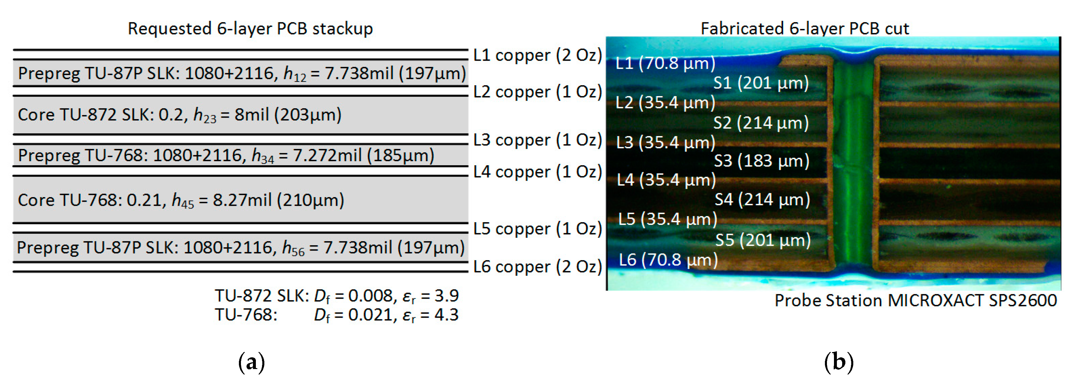
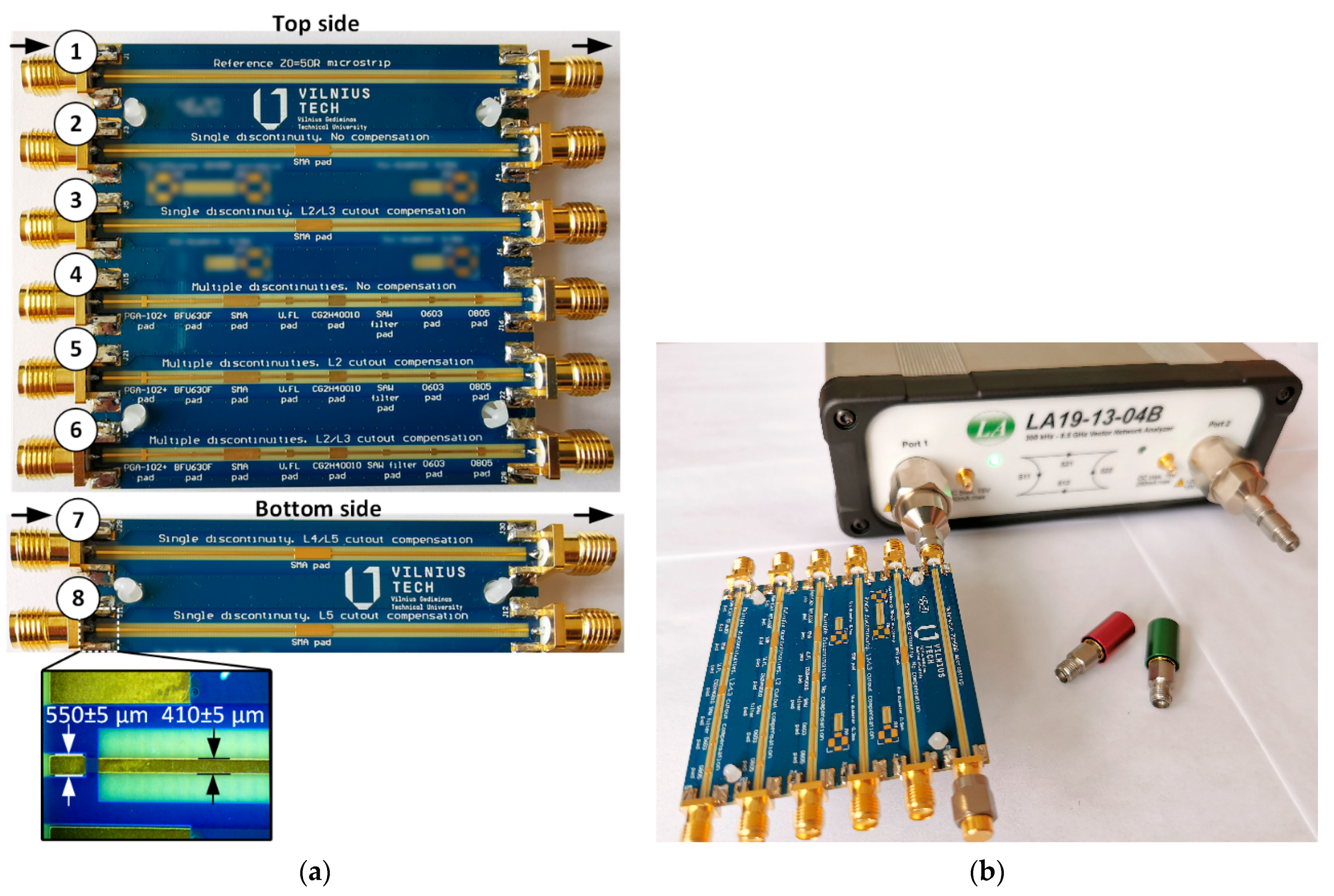
2. Target Design Scenario and DUT Description
3. Theoretical Evaluation
4. Measurements and Discussion
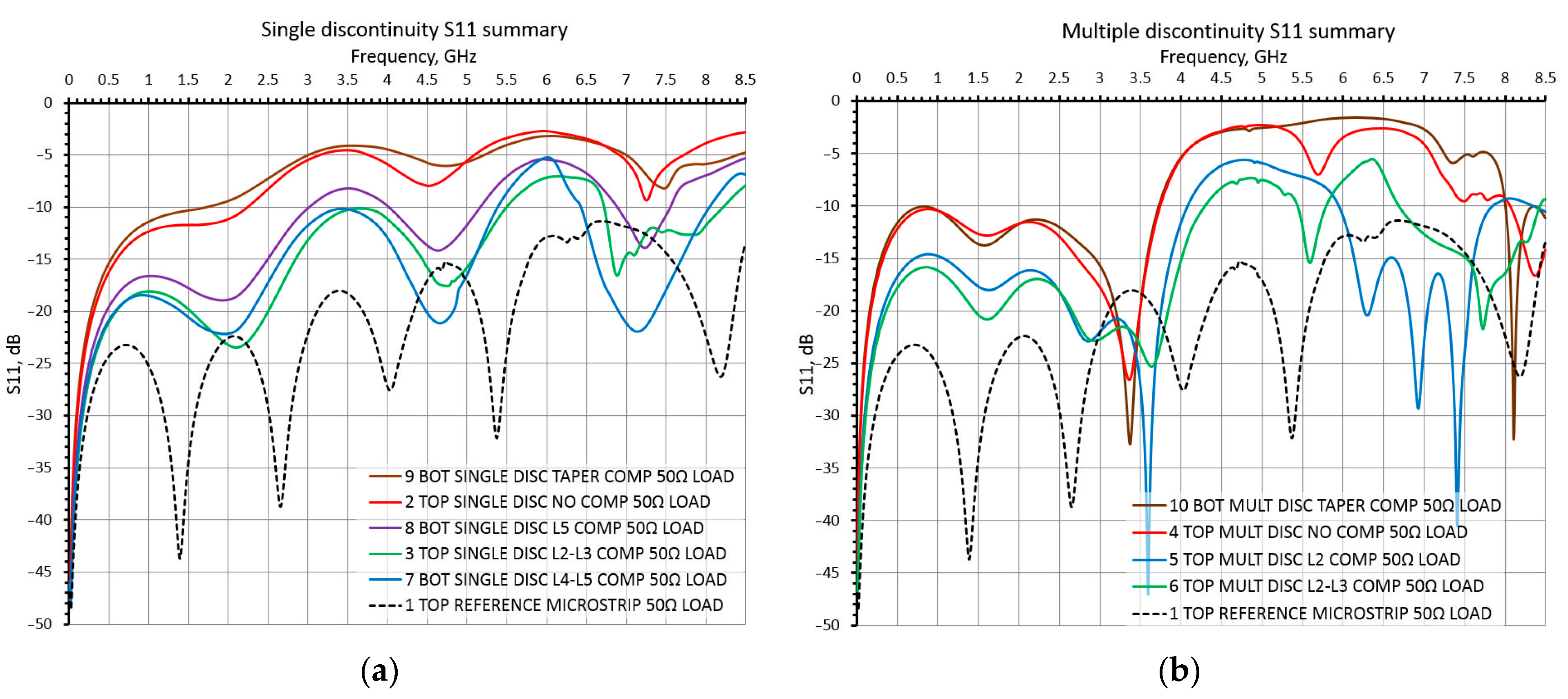
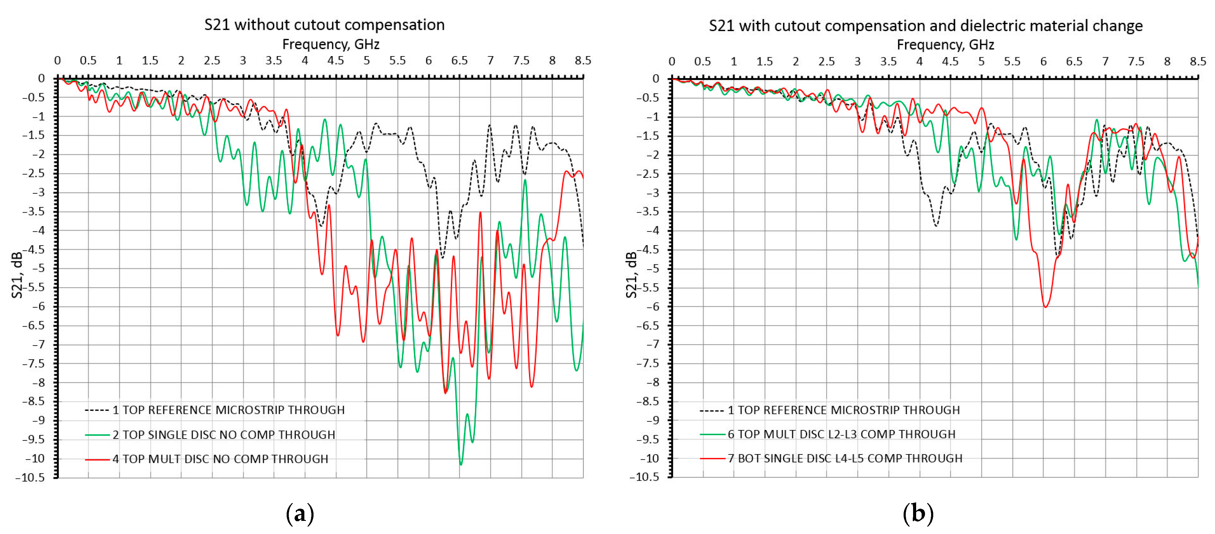
4.1. S-Parameter Measurement Results
4.2. TDR Measurements
4.3. Discussion
- Obtain an n-layer PCB with several types of laminates. The total required number of cutouts under a discontinuity has to be established (similar to results in Table 2). Thus, the capacitance-per-length, inductance-per-length, and effective dielectric permittivity are calculated using a model of choice (ex. according to Equations (3)–(5)) assuming there is only one type of dielectric.
- Calculate the intermediate impedance of the discontinuity according to Equation (2).
- Evaluate the total effective dielectric permittivity of the structure with the number of cutouts found in step 1 according to a model of choice for evaluating the total dielectric constant of multilayer substrates (ex. Equation (1)) and effective dielectric permittivity model of choice (ex. Equation (5)).
- Repeat the capacitance-per-length and inductance-per-length calculations in step 1 with the total effective dielectric permittivity found in step 3.
- Calculate the final impedance of the discontinuity with a multiple-laminate stack-up according to Equation (2).
5. Conclusions
Author Contributions
Funding
Institutional Review Board Statement
Informed Consent Statement
Data Availability Statement
Acknowledgments
Conflicts of Interest
References
- Pereira, A.; Romero, F. A review of the meanings and the implications of the Industry 4.0 concept. Procedia Manuf. 2017, 13, 1206–1214. [Google Scholar] [CrossRef]
- Weyer, S.; Schmitt, M.; Ohmer, M.; Gorecky, D. Towards Industry 4.0-Standardization as the crucial challenge for highly modular, multi-vendor production systems. IFAC-PapersOnline 2015, 48, 579–584. [Google Scholar] [CrossRef]
- Silva, M.M.D.; Guerreiro, J. On the 5G and Beyond. Appl. Sci. 2020, 10, 7091. [Google Scholar] [CrossRef]
- Gundall, M.; Strufe, M.; Schotten, H.D.; Rost, P.; Markwart, C.; Blunk, R.; Neumann, A.; Griebbach, J.; Aleksy, M.; Wubben, D. Introduction of a 5G-Enabled Architecture for the Realization of Industry 4.0 Use Cases. IEEE Access 2021, 9, 25508–25521. [Google Scholar] [CrossRef]
- Penttinen, J.T.J. 5G Explained: Security and Deployment of Advanced Mobile Communications; John Wiley & Sons Ltd.: Hoboken, NJ, USA, 2019. [Google Scholar]
- Ramzan, R.; Fritzin, J.; Dabrowski, J.; Svensson, C. Wideband Low-Reflection Transmission Lines for Bare Chip on Multi-layer PCB. ETRI J. 2011, 33, 335–343. [Google Scholar] [CrossRef]
- Pozar, D.M. Microwave Engineering, 4th ed.; John Wiley & Sons, Inc.: Hoboken, NJ, USA, 2012; pp. 261–267. [Google Scholar]
- Steer, M. Microwave and RF Design: Networks; Open Textbook Library: Minneapolis, MN, USA, 2019; pp. 217–225. [Google Scholar]
- Klopfenstein, R. A Transmission Line Taper of Improved Design. Proc. IRE 1956, 44, 31–35. [Google Scholar] [CrossRef]
- Collin, R.E. Foundations for Microwave Engineering; Wiley-Interscience: New York, NY, USA, 2001. [Google Scholar]
- Chen, S.; Liang, Z. The impedance matching analysis on different tapered line function. In Proceedings of the 4th IEEE International Conference on Broadband Network and Multimedia Technology 2011, Shenzhen, China, 28–30 October 2011. [Google Scholar]
- Cogollos, S.; Vague, J.; Boria, V.E.; Martinez, J.D. Novel Planar and Waveguide Implementations of Impedance Matching Networks Based on Tapered Lines Using Generalized Superellipses. IEEE Trans. Microw. Theory Tech. 2018, 66, 1874–1884. [Google Scholar] [CrossRef]
- Rizvi, S.A.P.; Khan, R.A.A. Klopfenstein tapered 2–18 GHz microstrip balun. In Proceedings of the 9th International Bhurban Conference on Applied Sciences & Technology (IBCAST), Islamabad, Pakistan, 9–12 January 2012. [Google Scholar]
- Vasjanov, A.; Barzdenas, V. Reduced-Reflection Multilayer PCB Microstrip with Discontinuity Characterization. Electronics 2020, 9, 1473. [Google Scholar] [CrossRef]
- Isola Group. PCB Laminate and Prepreg Materials. Available online: https://www.isola-group.com/pcb-laminates-prepreg/ (accessed on 27 August 2021).
- Rogers Corporation. Advanced Electronics Solutions: RF Solutions Laminates, Prepregs and Bondplys. Available online: https://rogerscorp.com/advanced-electronics-solutions (accessed on 27 August 2021).
- Taiwan Union Technology Corporation. Product Selector “View Products by Property”. Available online: http://www.tuc.com.tw/en-us/products2 (accessed on 27 August 2021).
- Hu, F.; Song, J.; Kamgaing, T. Modeling of multilayered media using effective medium theory. In Proceedings of the 19th Topical Meeting on Electrical Performance of Electronic Packaging and Systems, Austin, TX, USA, 25–27 October 2010; pp. 225–228. [Google Scholar] [CrossRef]
- Paul, C.R. Inductance Loop and Partial; Wiley: Hoboken, NJ, USA, 2010; p. 181. [Google Scholar]
- Paul, C.R. Analysis of Multiconductor Transmission Lines, 2nd ed.; Wiley: Hoboken, NJ, USA, 2008; pp. 146–147. [Google Scholar]
- Hammerstad, E.O.; Bekkadal, F. Microstrip Handbook; ELAB Report STF 44 A74169; The University of Trondheim: Trondheim, Norway, February 1975. [Google Scholar]
- Wadell, B.C. Transmission Line Design Handbook; Artech House: Boston, MA, USA, 1991. [Google Scholar]
- Antonovici, D. Advances in Time Domain Reflectometry characterisation for high speed interconnects. In Proceedings of the 2015 IEEE 21st International Symposium for Design and Technology in Electronic Packaging (SIITME), Brasov, Romania, 22–25 October 2015; pp. 37–40. [Google Scholar] [CrossRef]


| Microstrip Number in Figure 3 | Microstrip Location on PCB | Dielectric Material Change | DUT Layer-by-Layer Configuration Based on Figure 2 Segments (a, b, c, d, or e). |
|---|---|---|---|
| 1 | Top (L1) | No. TU-87P SLK | 50Ω reference line. L2—solid GND reference plane |
| 2 | No. TU-87P SLK | L1—a; L2—solid GND reference plane | |
| 3 | Yes. TU-87P SLK → TU-872 SLK → TU-768 | L1—a; L2 and L3—b; L4—solid GND reference plane | |
| 4 | No. TU-87P SLK | L1—c; L2—solid GND reference plane | |
| 5 | No. TU-87P SLK → TU-872 SLK | L1—c; L2—d; L3—solid GND reference plane | |
| 6 | Yes. TU-87P SLK → TU-872 SLK → TU-768 | L1—c; L2—d; L3—e; L4—solid GND reference plane | |
| 7 | Bottom (L6) | Yes. TU-87P SLK → TU-768 → TU-768 | L6—a; L5 and L4—b; L3—solid GND reference plane |
| 8 | Yes. TU-87P SLK → TU-768 | L6—a; L5—b; L4—solid GND reference plane |
| Pad Name | Pad from Component | Pad Area L × W, mm2 | Distance between Pad Centers | Zw/o comp., Ω | Z1-layer comp., Ω | Z2-layer comp., Ω |
|---|---|---|---|---|---|---|
| A0 | SMA 2.9 mm conn. | 1 × 0.55 | A0–A1: 31.7 mm A0–A8: 7.4 mm All others: 7 mm | 42.1743 1 | 67.61762 | 79.98712 |
| A1 | SMA 3.5 mm conn. | 5.2 × 1.5 | 19.9337 | 36.8572 | 47.2629 | |
| A2 | PGA-102+ | 0.7 × 1.6 | 18.9037 | 35.2163 | 45.3666 | |
| A3 | BFU630F | 0.55 × 0.6 | 39.7756 1 | 64.67512 | 77.07482 | |
| A4 | U.FL conn. | 1 × 1 | 27.4820 | 48.2386 1 | 59.97802 | |
| A5 | CG2H40010 | 2.5 × 1.5 | 19.9337 | 36.8572 | 47.2629 | |
| A6 | SAW filter | 1.05 × 0.8 | 32.4676 | 55.1932 1 | 67.38782 | |
| A7 | 0603 SMD | 0.8 × 0.9 | 29.7611 | 51.4696 1 | 63.45342 | |
| A8 | 0805 SMD | 1.1 × 1.2 | 23.8520 | 42.9011 | 54.1085 |
Publisher’s Note: MDPI stays neutral with regard to jurisdictional claims in published maps and institutional affiliations. |
© 2021 by the authors. Licensee MDPI, Basel, Switzerland. This article is an open access article distributed under the terms and conditions of the Creative Commons Attribution (CC BY) license (https://creativecommons.org/licenses/by/4.0/).
Share and Cite
Vasjanov, A.; Barzdenas, V. Microstrip Impedance Management through Multilayer PCB Stack-Up: Discontinuity Compensation Voids with Asymmetric Dielectrics. Symmetry 2021, 13, 1771. https://doi.org/10.3390/sym13101771
Vasjanov A, Barzdenas V. Microstrip Impedance Management through Multilayer PCB Stack-Up: Discontinuity Compensation Voids with Asymmetric Dielectrics. Symmetry. 2021; 13(10):1771. https://doi.org/10.3390/sym13101771
Chicago/Turabian StyleVasjanov, Aleksandr, and Vaidotas Barzdenas. 2021. "Microstrip Impedance Management through Multilayer PCB Stack-Up: Discontinuity Compensation Voids with Asymmetric Dielectrics" Symmetry 13, no. 10: 1771. https://doi.org/10.3390/sym13101771
APA StyleVasjanov, A., & Barzdenas, V. (2021). Microstrip Impedance Management through Multilayer PCB Stack-Up: Discontinuity Compensation Voids with Asymmetric Dielectrics. Symmetry, 13(10), 1771. https://doi.org/10.3390/sym13101771