1. Introduction
Conventional successive approximation analog-to-digital converter (SARADC) techniques require precise component matching to achieve high resolution and linearity. About ten years ago, SARADC began to dominate in low-power and low-speed applications. In recent years, there has been an increasing demand for high-speed, high-resolution, and low-power analog-to-digital converters for applications in many fields, particularly wireless communications, smart sensors, and biomedical technologies. The increasing improvement of Complementary Metal Oxide Semiconductor (CMOS) technologies has facilitated improvements in speed and energy efficiency and helped the SAR structure expand from low-speed applications into the medium- and even high-speed application domains, for which flash or pipeline architectures are traditionally designed. Moreover, the development of other technologies such as digital auxiliary calibration, excellent power saving and area reduction, time interleaving technology, and so on, have caused SAR architecture to become one of the most popular topologies, with an increasingly wide range of applications. However, ADCs in most systems typically require at least a 10-bits resolution and a sampling rate of hundreds of kHz, or even MHz. There are many factors that degenerate the performance of ADC, with comparator offset and capacitor mismatch making up the highest proportion.
Researchers hoping to achieve high-resolution and high-speed SARADC need to acknowledge that comparator offset may degrade the precision, which therefore must be considered. On the other hand, the
kT/C noise requirement can be fulfilled by using small capacitances. Parasitic capacitances and capacitor mismatch, along with small unit capacitors, will potentially cause the performance of ADCs to degenerate. Generally, capacitor mismatch can be classified into random and systematic mismatches. A substantial amount of work and research has been done to improve the dynamic and static performance. Currently, the primary method used to enhance the performance of SARADCs is the digital calibration technique [
1,
2,
3]. Some designs use digital tuning to eliminate the mismatches caused by parasitic capacitors, but they ignore the comparator offset. Another type of design decreases the offset by adding extra circuits, although this is at the expense of area and power consumption.
Accordingly, this paper presents a type of foreground digital calibration algorithm that can eliminate the comparator offset and capacitor mismatch, using the same extra circuits with minimal area and power consumption. A high precision full-scale differential dynamic comparator with a two-stage preamplifier was designed in combination with the calibration method. The design incorporates tri-level switching into capacitors based on
Vcm architecture, thereby achieving improved energy efficiency [
4]. The bottom plates of the capacitor array are used to sample the input signals so as to achieve better linearity, from
Vcm switching to
Vref or GND in each step, which can reduce switching energy usage. Moreover, the most significant bit (MSB) can be decided after sampling without any consumption of switching energy; thus, the total capacitor is halved, compared with conventional architecture, and the core area is also reduced. The topology of the whole SARADC is shown in
Figure 1.
The remainder of this paper is organized as follows:
Section 2 introduces the theory of the digital foreground calibration algorithm.
Section 3 describes the details of circuit implementation, which is followed by the simulation results in
Section 4. Finally, a brief conclusion is provided in
Section 5.
2. The Digital Foreground Calibration Algorithm
In this design, the calibration signal enables the determination of whether to begin work with the calibration mode or the conversion mode. When the reset signal and the calibration’s enabling signal are high at the same time, the converter begins work in calibration mode; after calibration mode is over, the calibration’s finishing signal changes from low to high, and conversion mode starts normally. If only the reset signal is high when the clock cycle is incoming, the converter begins work in conversion mode.
2.1. Comparator Offset
Comparator offset is typically a random additive error [
5]. In a single-channel ADC, the offset error produces a DC tone, and the comparator is usually designed to have input-referred noise of less than 1 LSB. For a low-power supply ADC, 1 LSB is equal to
Vref/2
N*bit. For example, for a 12-bit SARADC with a 1.2 V power supply, 1 LSB is equal to 293 µV. However, the offset error voltage of the comparator is usually larger than 5 mV. Therefore, this design proposes a self-calibration technique for digital-to-analog (DAC) mismatch, based on the comparator that requires the offset voltage to be minimized through self-calibration in advance. In this design, the comparator has a two-stage preamplifier to enhance precision. Post-simulation of the comparator layout shows that the difference of input minimum voltage is about 65 µV and can be compared, preceding the demand of the comparator self-calibration precision by about 1/4 LSB. Thus, meeting the requirement completely.
The basic idea behind the calibration algorithm is to deliberately introduce some imbalance to compensate for the offset. Capacitance loading, current injection, or even voltage difference may cause comparator imbalance. To minimize or even eliminate the voltage error, a certain common mode voltage is generally tied together to the differential inputs of the comparator, which should be kept constant when the ADC system is working normally; moreover, the output of the comparator is monitored, and feedback is sent to the state machine to control and minimize the imbalance. Capacitance loading is used to calibrate or minimize the comparator offset; moreover, through changing the load of capacitance, the current, or the threshold voltage, the offset error voltage can be compensated for through the differential output pair,
p_p and
p_n, of the second preamplifier. In order to reduce the voltage error caused by comparator offset, the proposed self-calibration techniques change the capacitance of the output node of the second preamplifier. The capacitor arrays used to control the capacitance of the preamplifier output pair consist of Metal Oxide Semiconductor (MOS) capacitors and use Positive channel Metal Oxide Semiconductor (PMOS) transistors, as shown in
Figure 2. Each node has eight MOS capacitors arrays (
Cp<0> ~
Cp<7>;
Cn<0> ~
Cn<7>). The calibration capacitor arrays are binary-weighted, like the capacitor array of the main DAC in SARADC, while the unit capacitance size is as small as possible.
The calibration MOS capacitances are binary-weighted, and every capacitance can calibrate offset voltage equal to 1/4 LSB; thus, the total approaches 64 LSB. Both the global reset signal, Rst, and the calibration enabling signal, cal_en, are high, the self-calibration mode for the comparator is selected, the SAR control logic is disconnected from the main DAC driver, and the two inputs of the comparator connect with common voltage, Vcm. PMOS capacitance is added until the comparator output turns; the offset error is less than 1/4 LSB, and there is minimal impact on the performance of the whole ADC.
2.2. Capacitor Mismatch
We consider the parasitic capacitances on both the top and bottom plates of the capacitor array from non-ideal layout and wiring inevitability, the channel capacitance of MOS switches, and the gate capacitances of the comparator. The parasitic capacitances on the bottom plate of the capacitor array are driven by low impedance reference supplies. However, as long as the reference voltages are completely settled, they do not affect the conversion process or the result. Moreover, the parasitic capacitance on the top plate of the capacitor array attenuates the amplitude of the sampled input signal; this attenuation does not change the polarity of the comparison result, but does reduce the effective signal power, which is relevant information for determining the correct output bit. It is essential, for the bottom plate sampling, to enable this feature. In the sampling phase, the top plate of the capacitor array is pre-charged to Vcm by connecting with the common voltage, before the node becomes disconnected and remains disconnected until the conversion process is over. During the conversion process, the top plate voltage moves, but eventually returns to a constant value that is close to Vcm at the end of the process. Finally, the total charge of the parasitic capacitances is the same from the beginning to the end of the process. From the perspective of charge, parasitic capacitances do not cause voltage error. Accordingly, the parasitic capacitances on the top plate of the capacitor array do not affect the overall accuracy of the conversion process.
By contrast, mismatch errors are inevitable due to process variations, especially in the design of a capacitor array-based SARADC. Capacitor array mismatch is the main cause of the voltage error in the conversion process. In order to improve the performance of ADCs, this paper presents a foreground digital self-calibration technique for DAC capacitor mismatch, based on the comparator.
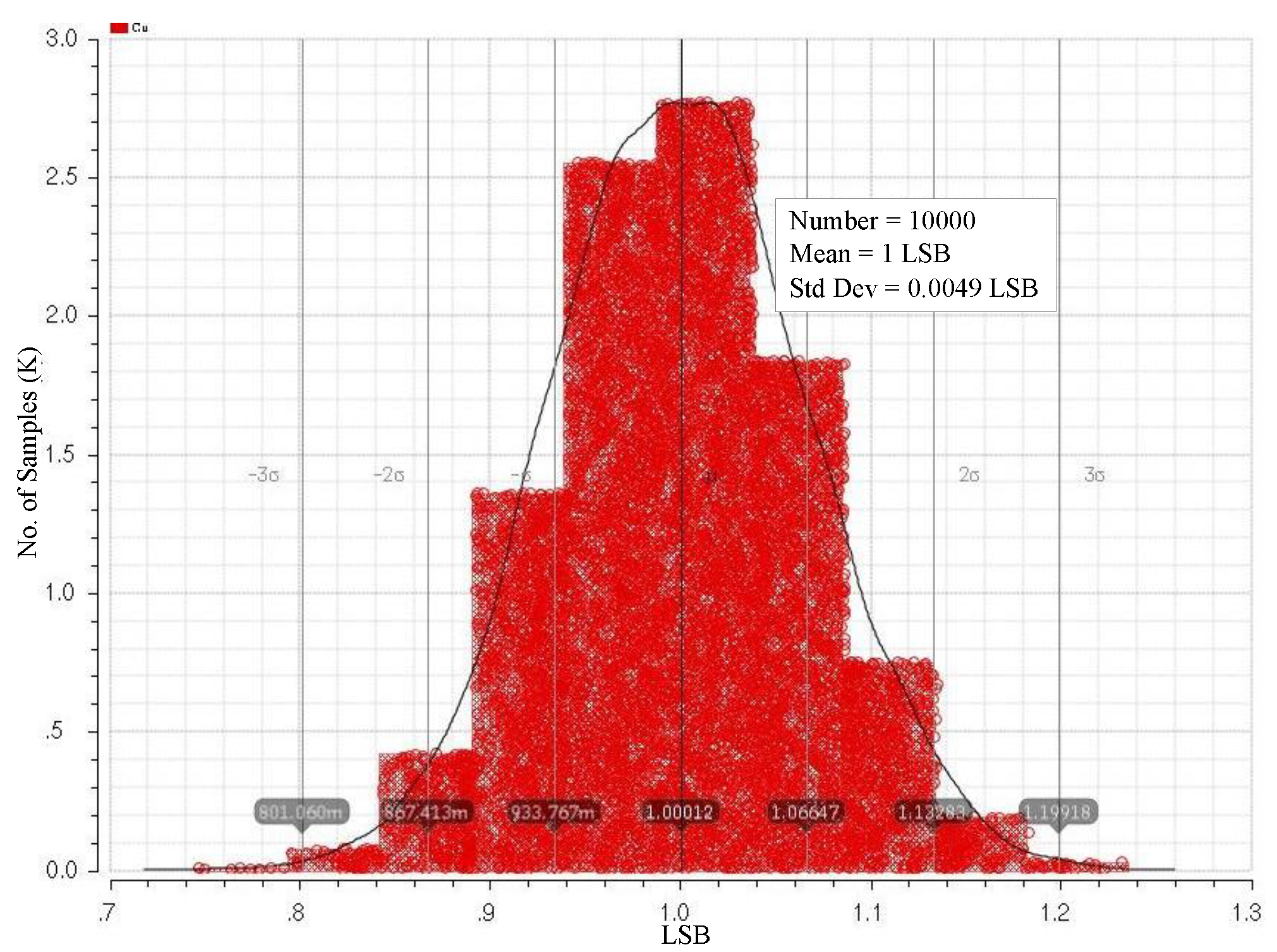
Figure 3 shows the histogram of the Metal–Oxide–Metal (MOM) unit capacitor subject to process mismatch, using a 10k-point Monte Carlo simulation. It must be ensured that the maximum voltage error caused by the mismatch of the MOM capacitor array can be calibrated with the MOS capacitor array. The schematic of the comparator with the calibration capacitor array is presented in
Figure 2.
2.3. The Calibration Theory
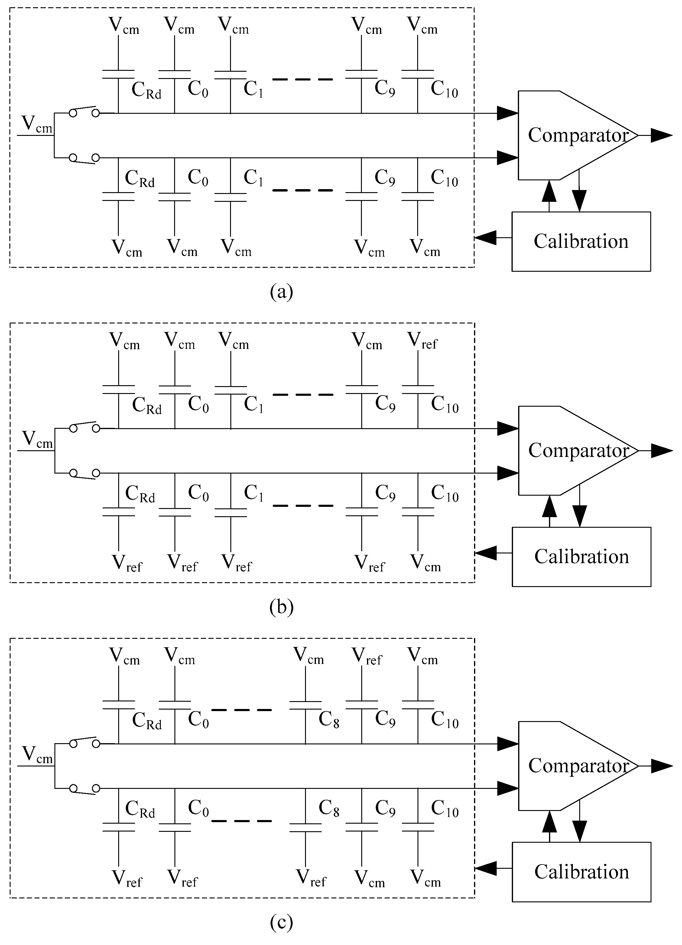
The calibration process is similar to the normal conversion process. At the sampling stage, both the top and bottom plates of the capacitor array are connected with common voltage,
Vcm; when the sampling phase is finished, the top plate of the capacitor array is disconnected with common voltage,
Vcm. Both the bottom plates of the positive and negative capacitor arrays are constantly connected with common voltage,
Vcm, as shown in
Figure 4a. The calibration MOS capacitor is then added to the positive or negative side, according to the feedback of the output of the comparator, and the code is restored until the comparator’s output changes; this step constitutes the calibration comparator offset for the MSB decision. The voltage for both positive and negative comparator inputs is as given in Equation (1):
Cu represents the ideal unit capacitor, and C0 = CRd = Cu; Ci = 2i·Cu; δ0 is the mismatch of the unit capacitor; and δi is the mismatch of the capacitor array, Ci. Based on Equation (1), mismatch is the main reason leading to voltage error.
The second step in sampling is similar to the first step: When the sampling is finished, the top plate of the capacitor array is disconnected from common voltage,
Vcm; both the bottom plate of
C10 in the positive capacitor array and the bottom plates (except
C10) in the negative array change from common voltage,
Vcm, to reference voltage,
Vref, at the same time; moreover, the rest of the capacitor array’s bottom plates connected with common voltage,
Vcm, remain unchanged. The process is as shown in
Figure 4b, and as given in Equations (2) and (3):
The third step is similar to the second step: When the sampling is finished, the top plate of the capacitor array is disconnected from common voltage,
Vcm; both the bottom plate of
C9 in the positive capacitor array and the bottom plates (except
C9) in the negative array change from common voltage,
Vcm, to reference voltage,
Vref, at the same time; moreover, the rest of the capacitor array’s bottom plates connected with common voltage,
Vcm, remain unchanged. The process is as shown in
Figure 4c, and as given in Equations (4) and (5):
The calibration process is repeated until capacitor array, C6, is calibrated. The maximum voltage error probably caused by capacitor array, C6, is less than half of LSB; it can thus completely satisfy the demands of a 12-bit SARADC.
After the calibration process is over, the signal of the calibration finish flag becomes high, and the ADC goes through the normal conversion process. The whole schematic of the comparator is as shown in
Figure 5, and as a symbol in
Figure 4.
2.4. Linearity Analysis
The voltage error caused by capacitor mismatch can be written as:
The variance of integral nonlinearity (INL) can be written as:
Consider the end point normalization:
Therefore, when
y = 2
N−2 is the maximum standard deviation, then
Therefore, MSB is independent of mismatch. When the output code changes from (001...1) to (010...0), or from (101...1) to (110...0), differential nonlinearity (DNL) reaches the maximum and the variance can be written as:
Therefore, the maximum standard deviation of DNL is:
The foreground digital calibration algorithm can greatly reduce the capacitor mismatch, reduce the linearity error, and improve the linearity.
3. Circuit Implementation
The DAC of an N-bit charge redistribution SARADC is composed of 2N−1 binary-weighted unit capacitor arrays that are multiples of the unit capacitor Cu (Cu, 2·Cu, 4·Cu ... 2N−2·Cu). A redundant unit capacitor CRd (CRd = Cu) is added to the array to make the number of capacitors a multiple of two, so that the total capacitance becomes 2N−1·Cu; the redundant unit capacitor is sampled together with the other capacitor arrays, but does not take part in the process of quantization. The Vcm-based capacitive structure SARADC only uses half as many unit capacitors, compared with conventional architecture; moreover, for a 12-bit SARADC, the Vcm-based tri-level switch structure saves about 87.51% in terms of switching energy consumption.
Two-Stage Preamplifier Full-Scale Differential Dynamic Comparator
The comparator is one of the most important components in high-resolution SARADC, as the precision of the comparator directly impacts the ADC performance. In this approach, the comparator is designed with a two-stage full-scale differential preamplifier and one latch, for high speed and high resolution. The preamplifier is used to amplify the input signal enough to satisfy the resolution requirement and block the kickback noise. The first-stage preamplifier supplies enough gain to enable high resolution, while the second-stage preamplifier supplies gain of approximately one to ensure the comparator achieves normalization in the full-scale swing input signal. Although the output signal of the preamplifier is larger than the input signal, it is still not large enough to drive the digital circuit; accordingly, a track and latch stage is designed to amplify the signal via a positive feedback loop. The comparator structure is as shown in
Figure 5.
The offset voltage,
Voffset, of the comparator can be calculated as:
where
represents the threshold mismatch,
VTH1,2 represents the threshold voltage,
represents the physical dimension mismatch between M
1 and M
2, and
represents the load resistance mismatch.
The noise of the comparator is the main factor that limits performance in a low-voltage-supply and high-speed SARADC design. The input-referred offset voltage of the comparator can directly affect the DC and AC performance of the converter. Moreover, a device mismatch such as threshold voltage, W/L, and/or
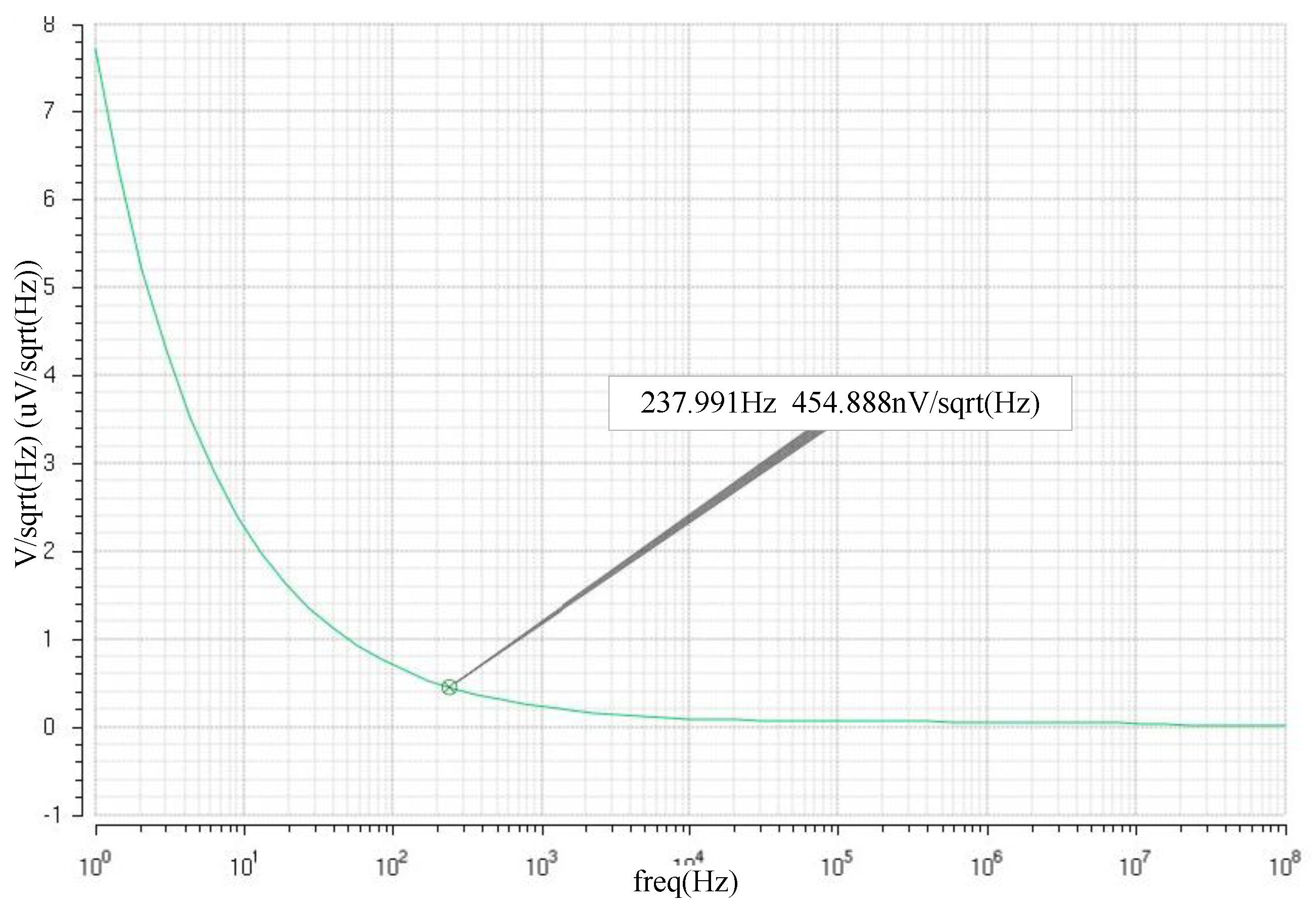
μCox variation may cause input-referred offset for the latch. The threshold voltage mismatch of the input transistors is the primary cause of comparator offset, which is inversely proportional to the gate area. Thus, the latch must be driven by a preamplifier to reduce the input-referred offset. To overcome the input-referred offset of the latch, the preamplifier circuit must supply enough gain to resolve the minimum difference of the input signal and amplify it to a large enough voltage. Accordingly, the comparator circuit offset is stored and canceled without adding any extra timing, by using this preamplifier. The input noise of the comparator is as shown in
Figure 6.
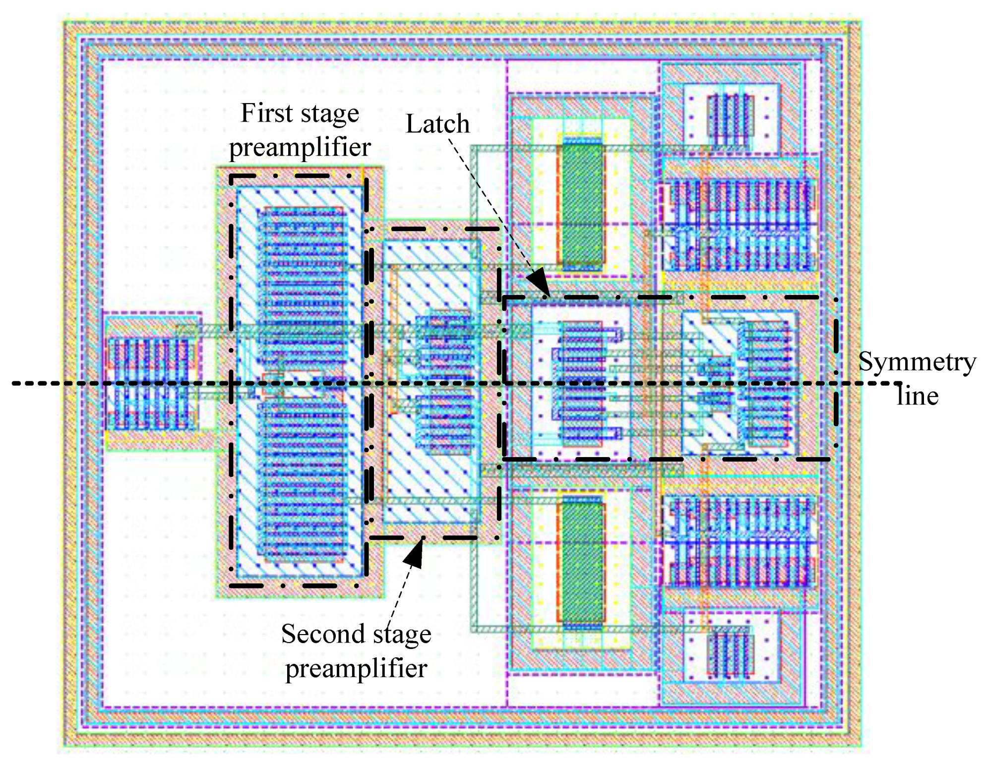
Finally, placement is important for the comparator layout. Symmetry is the most important rule in this context; a voltage difference of about 65 μV can be compared for the comparator layout post-simulation, completely satisfying the comparator requirement for the 12-bit SARADC. The comparator layout is depicted in
Figure 7.
4. Simulation Results
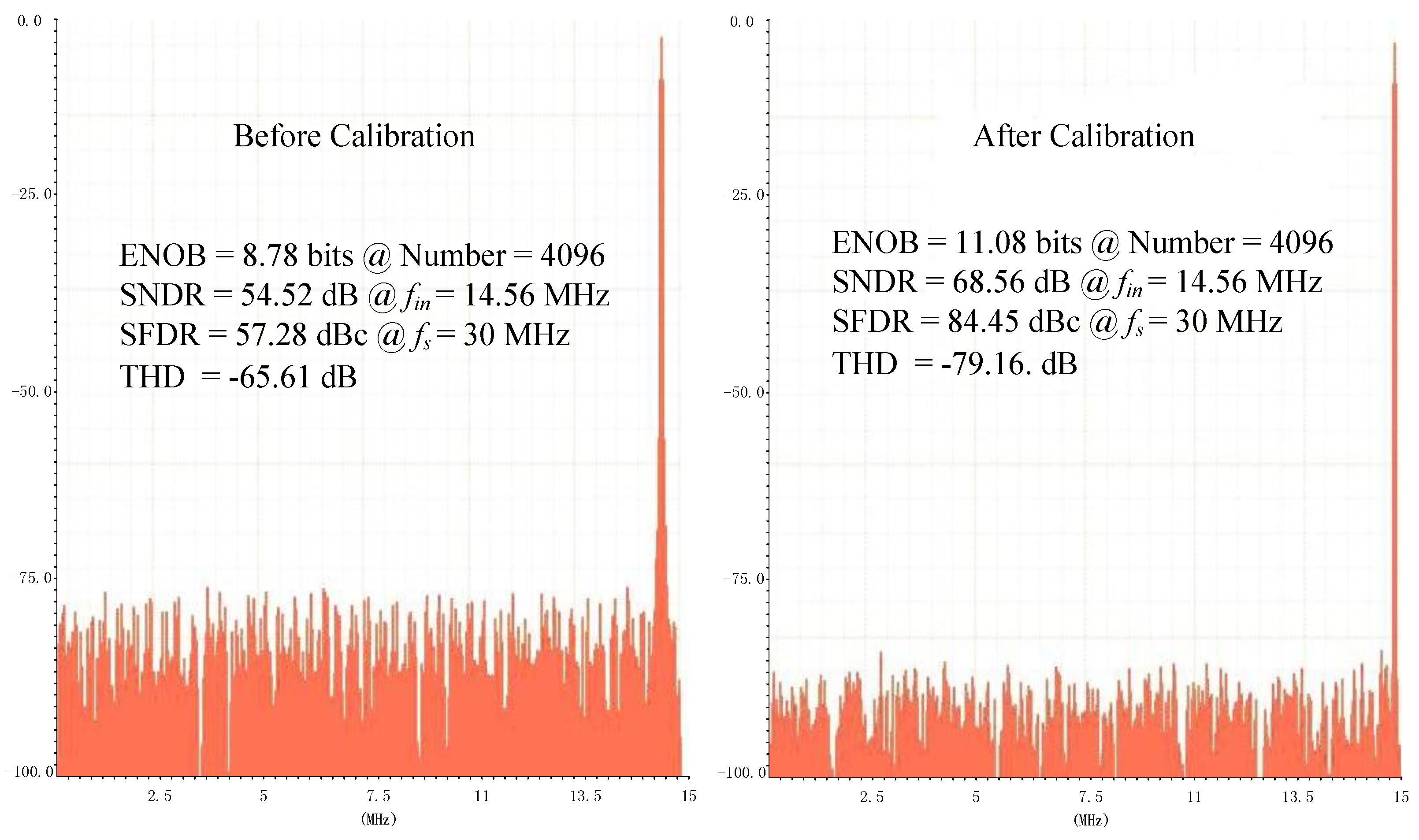
While the ADC operates at 30 Million Samples Per Second (MSPs), a 14.56 MHz full-scale sine wave input signal is used to test the dynamic and static performance.
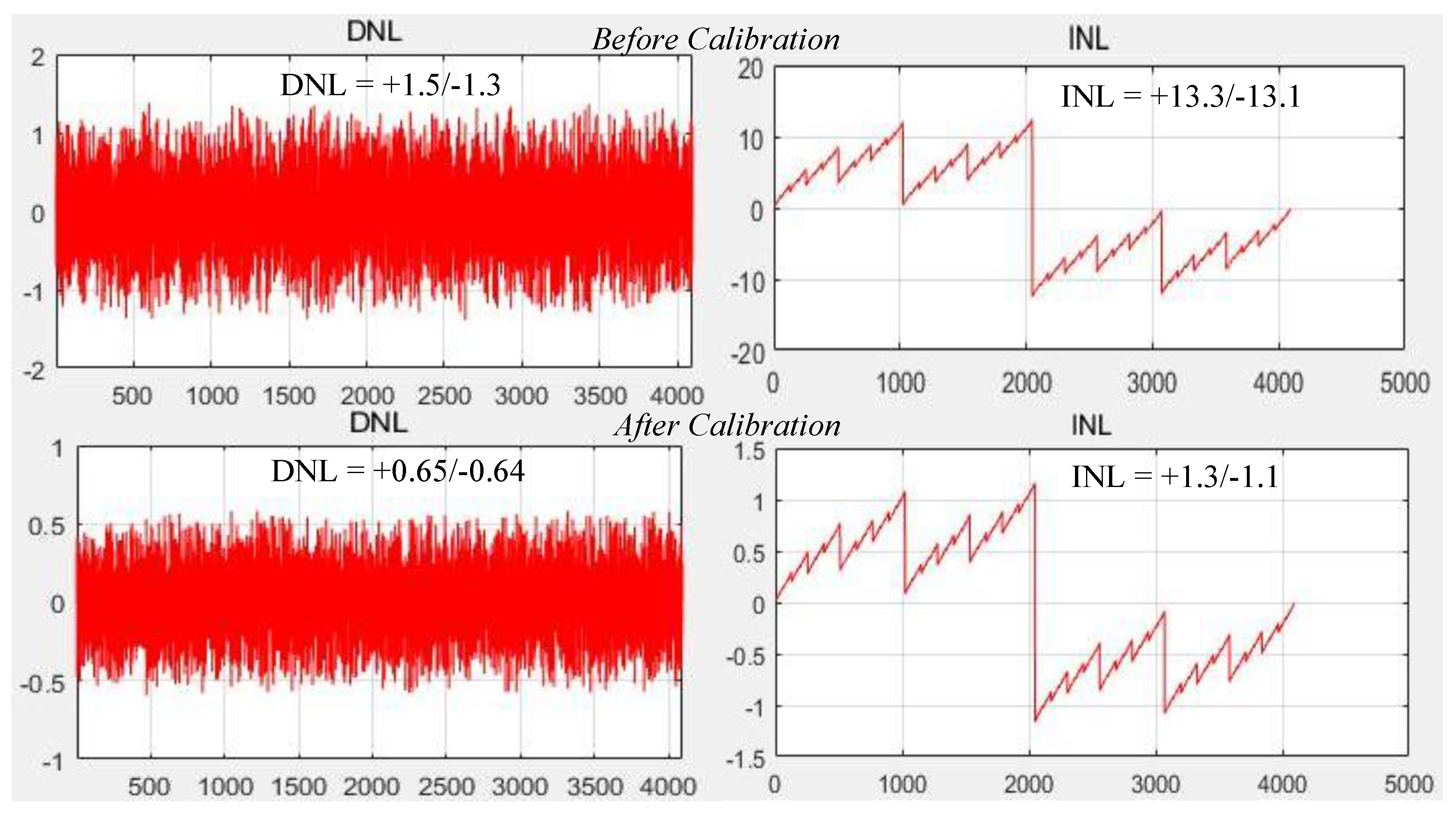
Figure 8 shows the DNL and INL simulation results before and after calibration. Before calibration, the maximum DNL is +1.5/−1.3 LSB, while the maximum INL error is +13.3/−13.1 LSB; after calibration, the maximum DNL and INL errors are +0.65/−0.64 LSB and +1.3/−1.1 LSB, respectively.
The dynamic performance based on a 4096-points Fast Fourier Transform (FFT), is as shown in
Figure 9. Before calibration, the signal-to-noise-and-distortion ratio (SNDR) and the spurious free dynamic range (SFDR) were 54.52 dB and 57.28 dBc, respectively, and the effective number of bits (ENOB) was 8.78. After calibration, the ADC achieves an SNDR of 68.56 dB, an SFDR of 84.45 dBc, and an ENOB of 11.08. The total power consumption consists of the estimated calibration, with a reference power of 2.39 mW, and a figure-of-merit (FoM) of 39.45 fJ/conv.-step.
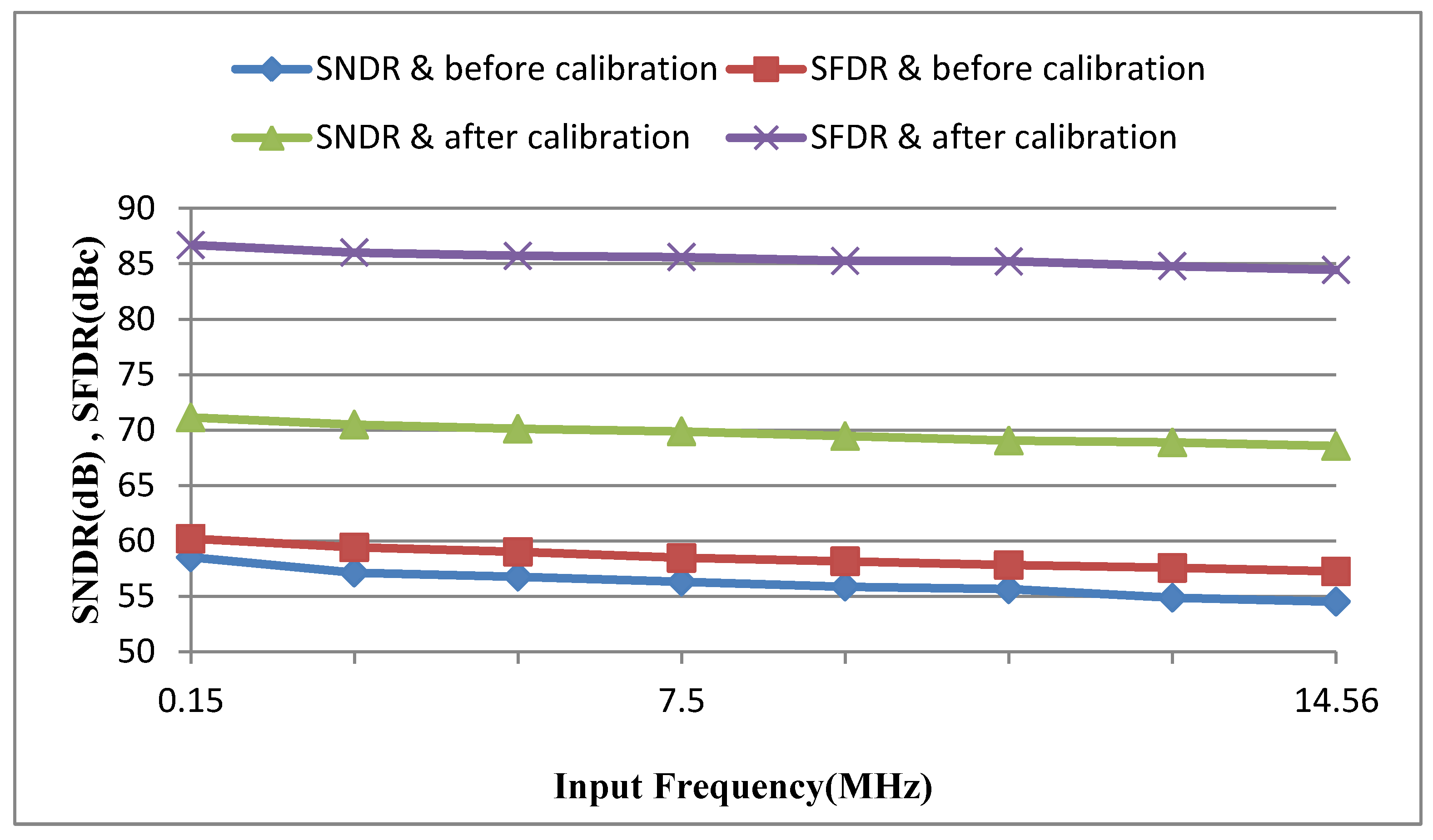
Figure 10 shows the simulation results of the SNDR and SFDR range, with input frequency before and after calibrations at a constant sampling rate of
fs = 2 MS/s.
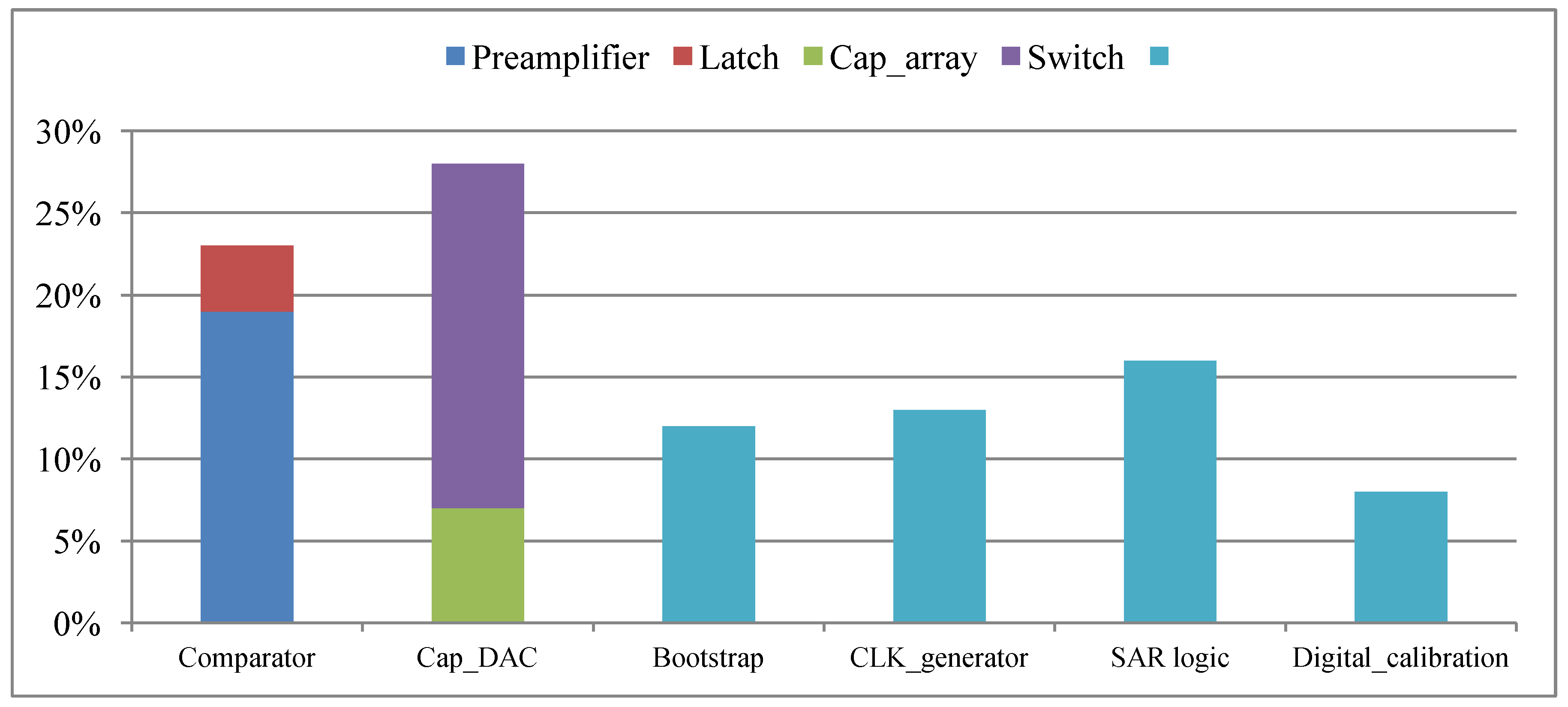
The breakdown of the power consumption at a sampling rate of
fs = 2MS/s is shown in
Figure 11. The comparator, capacitor digital-to-analog converter (CDAC), and SAR control logic power consumption, form the majority of the ADC power consumption. Preamplifier power consumption accounts for most of the power of the comparator. Switches always change from
Vcm, to
Vref or GND, and a great deal of energy will be used in this process. Bootstrap, Clock generator, and the digital calibration block only use a small amount of energy, which shows that the foreground digital calibration algorithm does not significantly increase power consumption.
Table 1 presents the performance comparison of this design with other published SARADCs, using a standard 0.13 μm CMOS process.
Ref. [
6] designed an asynchronous SARADC with multistep addition-only digital error correction (ADEC), additional decision phases incorporating DAC rearrangement with three sub-DACs, enhanced speed by 37%;
Table 1 shows the measured performance. Ref. [
7] designed a dual-tail instantaneous switching scheme using two capacitive DAC arrays, to generate two possible outputs while the comparator is in the regeneration process, and two binary redundancies to improve the overall conversion speed; the simulated performance is shown in
Table 1. Both designs were implemented in the CMOS 0.13 μm process. Ref. [
1] adopted an efficient on-chip foreground calibration algorithm and compensated the errors in digital domain normal operation;
Table 1 shows the measurement results. Ref. [
3] designed a dither-based background calibration technique to obtain an accurate comparator decision time (CDT) detection window size and ensure PVT robustness;
Table 1 shows the measurement results.
Moreover,
Table 2 presents the performance summary of the proposed ADC.
5. Conclusions
This paper has presented a foreground digital calibration algorithm, based on a comparator, to reduce the comparator offset and capacitor array mismatch, as well as enhance the performance of the whole ADC. The design adopts a fully differential topology with an incremental converting procedure, reducing the power consumption of DAC switching, the dynamic comparator, and asynchronous SAR control logic. A two-stage preamplifier full-scale differential dynamic comparator was designed for the calibration method. The reference voltage, Vref, of the DAC was set to supply voltage VDD to achieve rail-to-rail sampling.
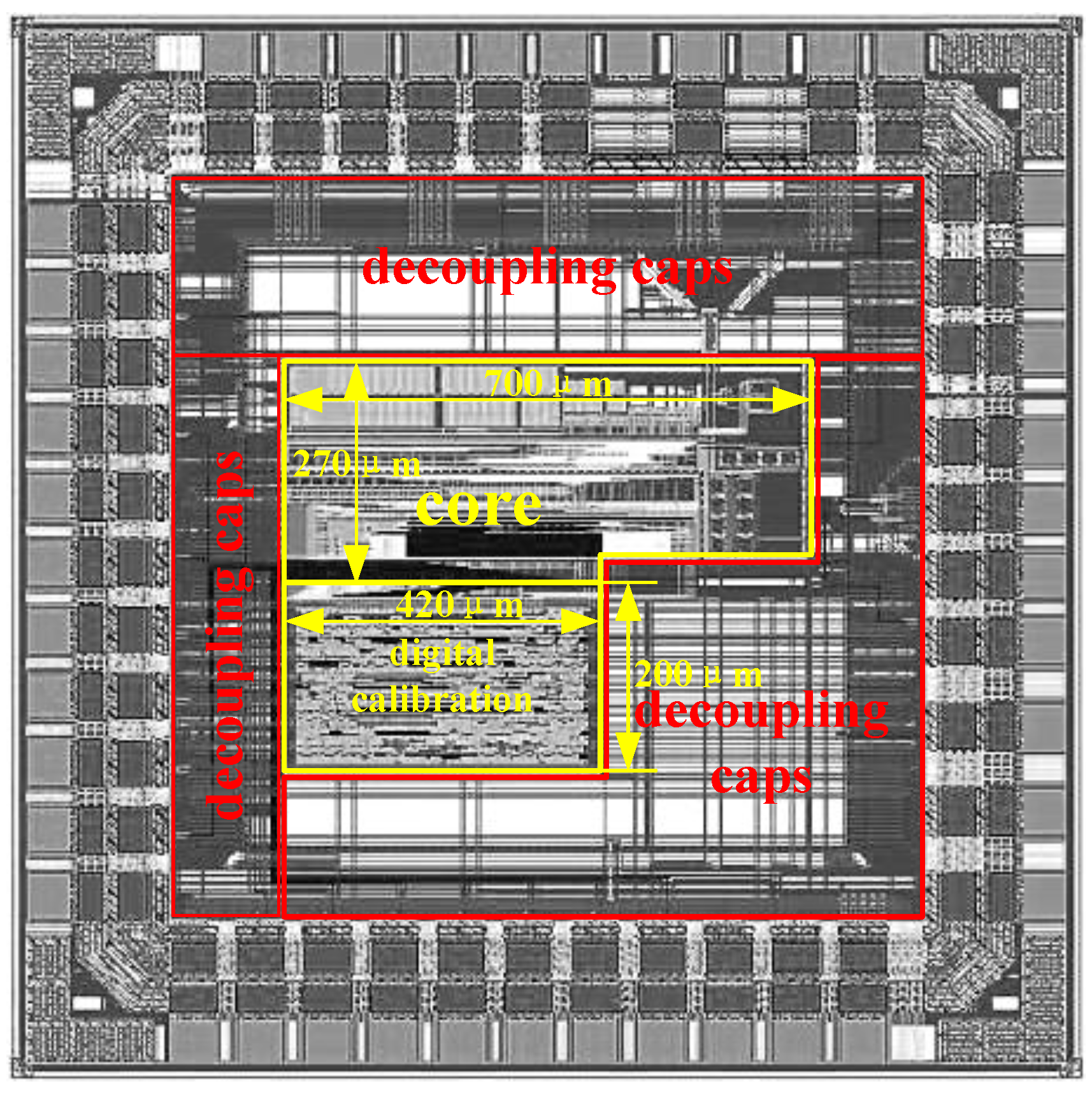
This ADC was designed and implemented with a one-poly-eight-metal (1P8M) 0.13 μm standard CMOS process. The die micrograph of the whole SARADC test chip is as shown in
Figure 12. The active area of the whole ADC is 0.273 mm
2. All capacitors were implemented using MOM structures. The digital calibration logic was based on a comparator MOS capacitor array and synthesized using Design Compiler, with an estimated area of 0.084 mm
2. The power supply is 1.2 V. At a 30 MS/s conversion rate, this SARADC achieved a state-of-the-art ENOB of 11.08 at a 14.56 MHz full-scale sine wave input frequency, resulting in a 39.45 fJ/conversion-step.
Author Contributions
S.L. designed the ADC and setup, performed the experimental work, performed Monte Carlo simulations, collated experimental data, organized the paper content, and wrote the manuscript. Y.G. performed supervision and funding acquisition. J.C. provided the idea of foreground digital calibration algorithm for comparator offset and capacitor mismatch, and performed analysis on the comparator offset calibration. B.L. performed project administration. All authors have read and agreed to the published version of the manuscript.
Funding
This research was funded by the National Natural Science Foundation of China Program, under Grant 61772540 and Grant 61974163.
Acknowledgments
This research was supported by the Graduate Innovation Center for Microelectronics and Microprocessors and funded by the National Natural Science Foundation of China Program.
Conflicts of Interest
The authors declare no conflict of interest.
References
- Shen, J.; Shikata, A.; Fernando, L.D.; Guthrie, N.; Chen, B.; Maddox, M.; Mascarenhas, N.; Kapusta, R.; Coln, M.C.W. A 16-bit 16 MS/s SAR ADC with on-chip calibration in 55 nm CMOS. IEEE J. Solid-State Circuits. 2018, 53, 1149–1160. [Google Scholar] [CrossRef]
- Fan, H.; Li, J.; Feng, Q.; Diao, X.; Lin, L.; Zhang, K.; Sun, H.; Heidari, H. Exploiting Smallest Error to Calibrate Non-Linearity in SAR Adcs. IEEE Access 2018, 6, 42930–42940. [Google Scholar] [CrossRef]
- Yoon, Y.; Sun, N. A 6-bit 0.81-mW 700-MS/s SAR ADC with sparkle-code correction, resolution enhancement, and background window width calibration. IEEE J. Solid-State Circuits 2018, 53, 789–798. [Google Scholar] [CrossRef]
- Yuan, C.; Lam, Y. Low-energy and area-efficient tri-level switching scheme for SAR ADC. Electron. Lett. 2012, 48, 482–483. [Google Scholar] [CrossRef]
- Tang, X.; Chen, L.; Song, J. A 1.5fJ/conv-step 10b 100kS/s SAR ADC with gain-boosted dynamic comparator. In Proceedings of the IEEE Asian Solid-State Circuits Conference: ASSCC 2017, Seoul, Korea, 1–4 November 2017. [Google Scholar]
- Cho, S.; Lee, C.; Kwon, J.; Ryu, S. A 550-μW 10-b 40-MS/s SAR ADC with Multistep Addition-Only Digital Error Correction. IEEE J. Solid-State Circuits 2011, 46, 1881–1892. [Google Scholar] [CrossRef]
- He, L.; Yang, J.; Luo, D.; Jin, L.; Zhang, S.; Lin, F.; Yao, L.; Jiang, X. A speed-enhancing dual-trial instantaneous switching architecture for SAR ADCs. IEEE Trans. Circuits Syst. II Express Briefs 2015, 62, 26–30. [Google Scholar] [CrossRef]
© 2020 by the authors. Licensee MDPI, Basel, Switzerland. This article is an open access article distributed under the terms and conditions of the Creative Commons Attribution (CC BY) license (http://creativecommons.org/licenses/by/4.0/).


