

Evaluation of Potential Occupational Exposure and Release of Nanoparticles in Semiconductor-Manufacturing Environments


Abstract
1. Introduction
2. Materials and Methods
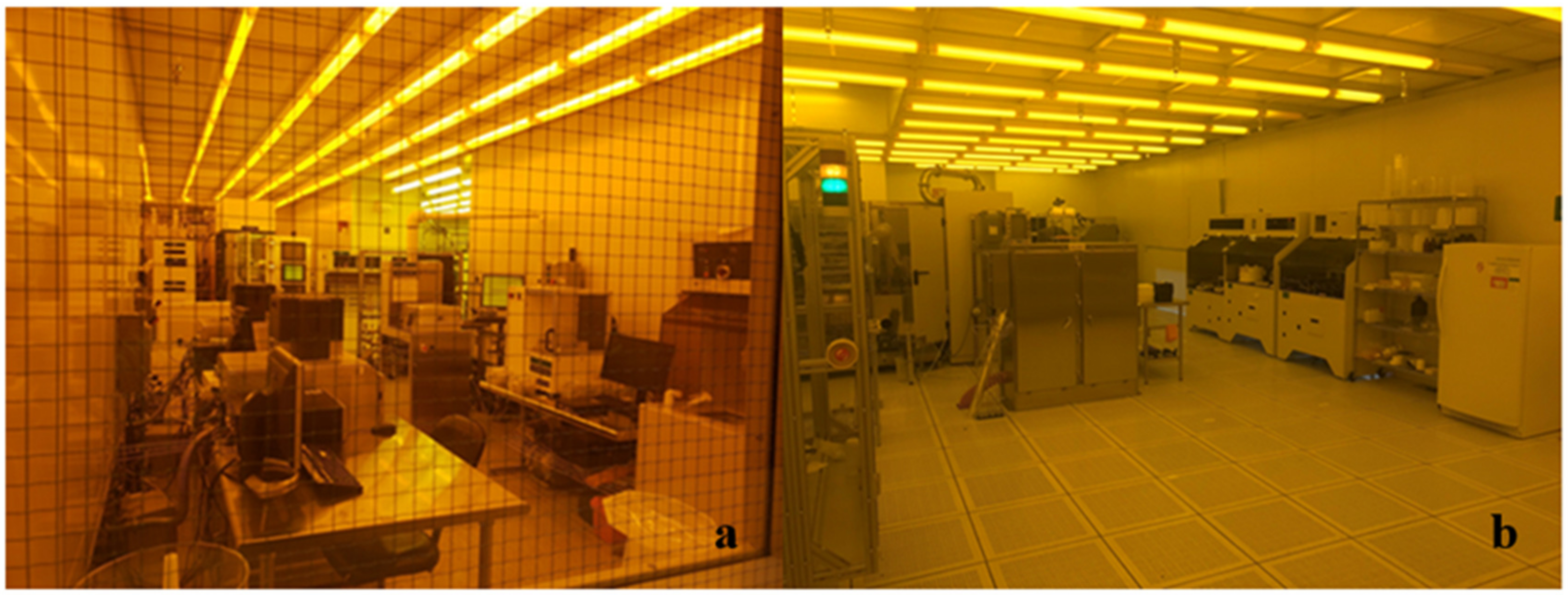
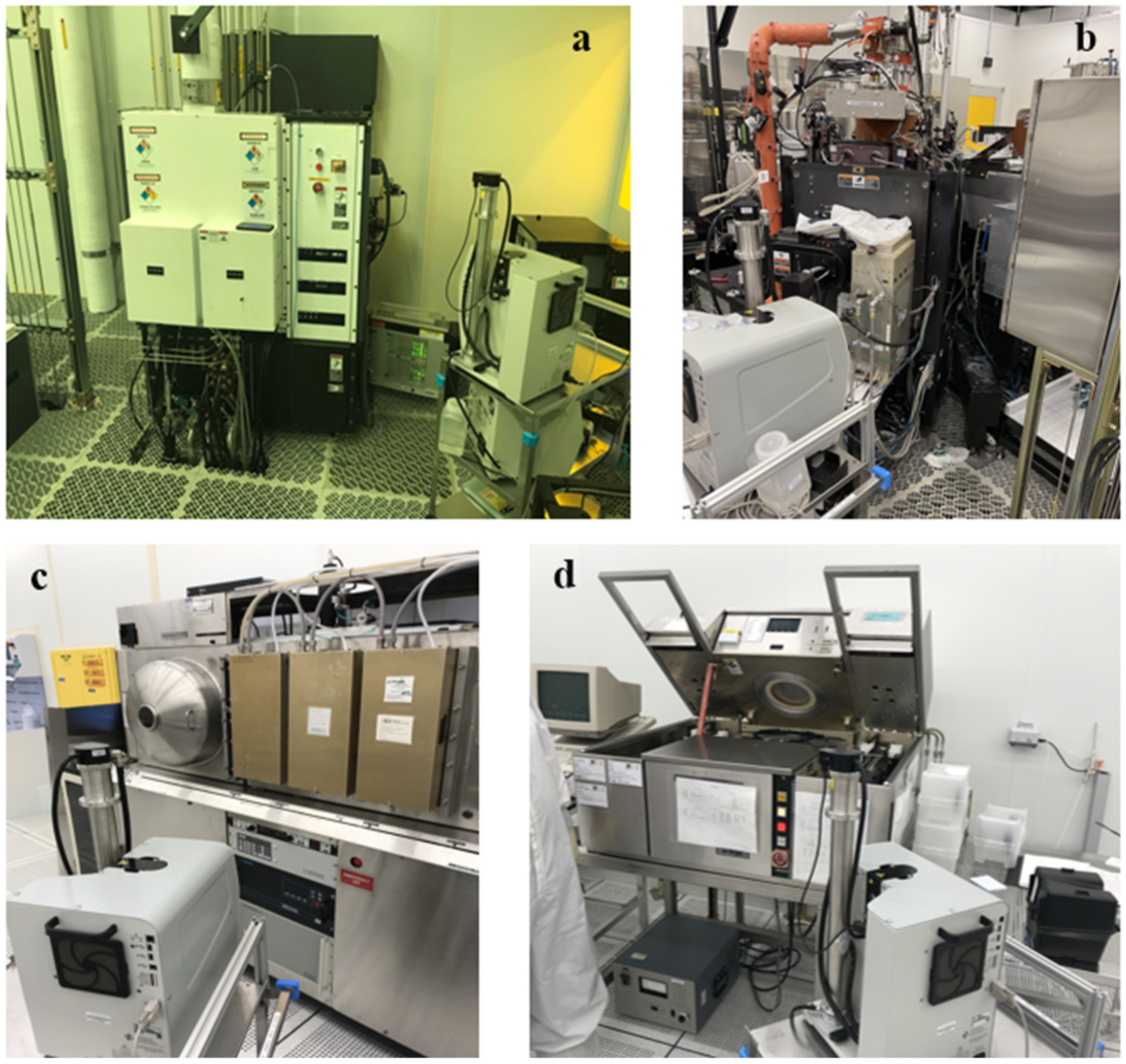
2.1. Sampling Site
2.2. Field Observations
2.3. Filter-Based Sample Collection
2.4. ICP-MS Analysis
2.5. STEM Analysis
3. Results and Discussion
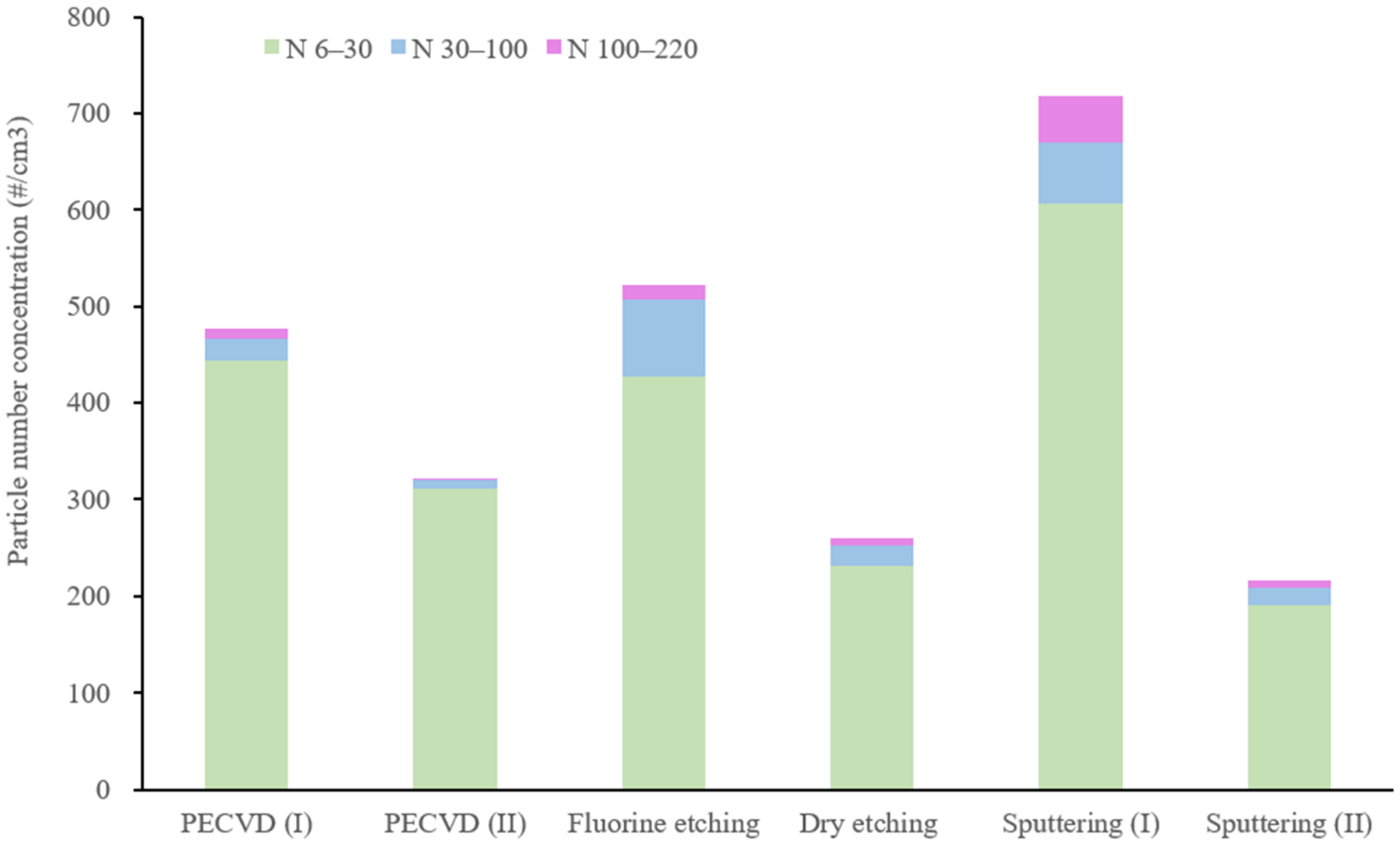
3.1. Particle Number Concentration
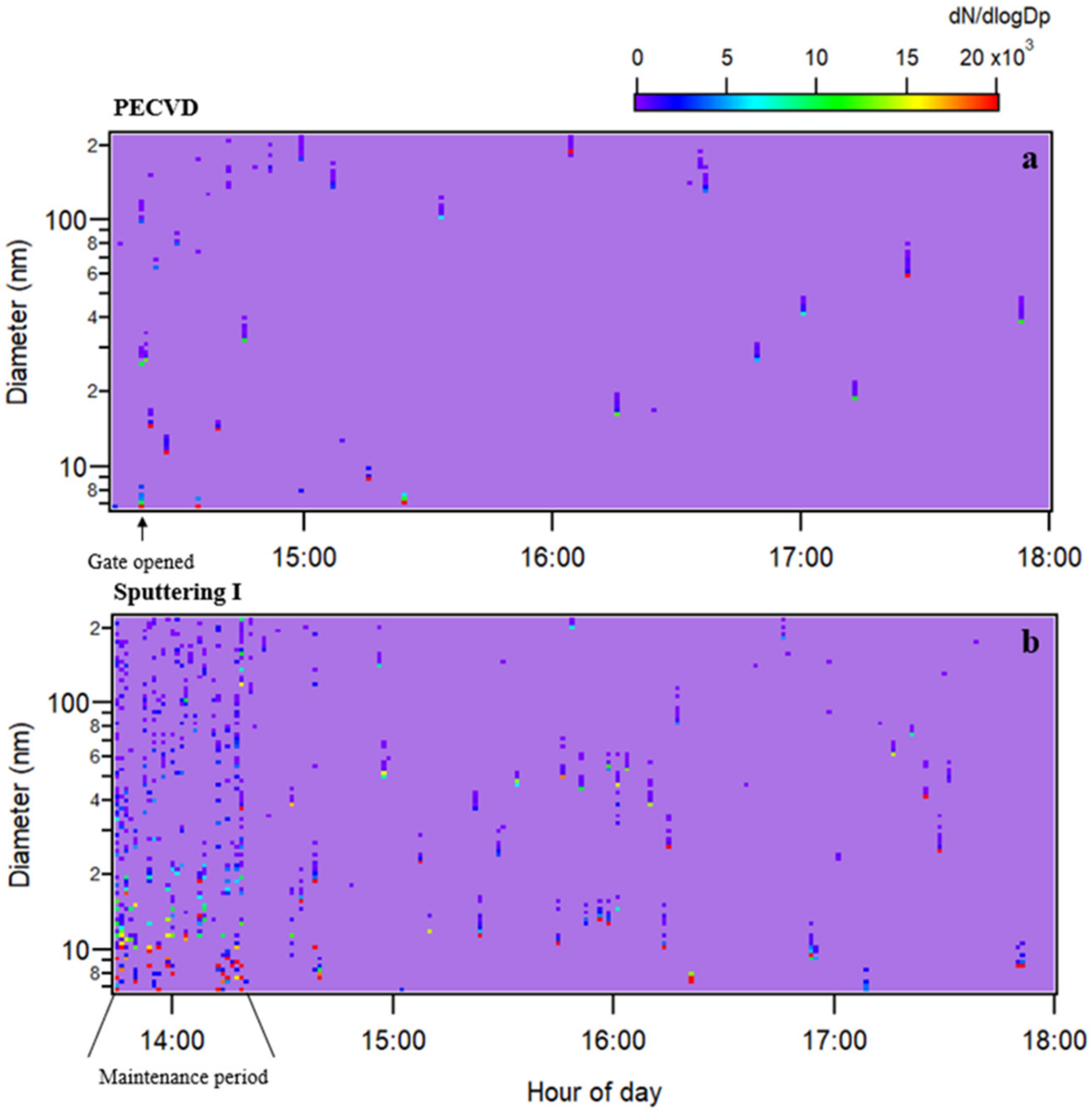
3.2. Particle Concentration Temporal Change during Maintenance
3.3. Particle Size Distribution for Airborne Particles
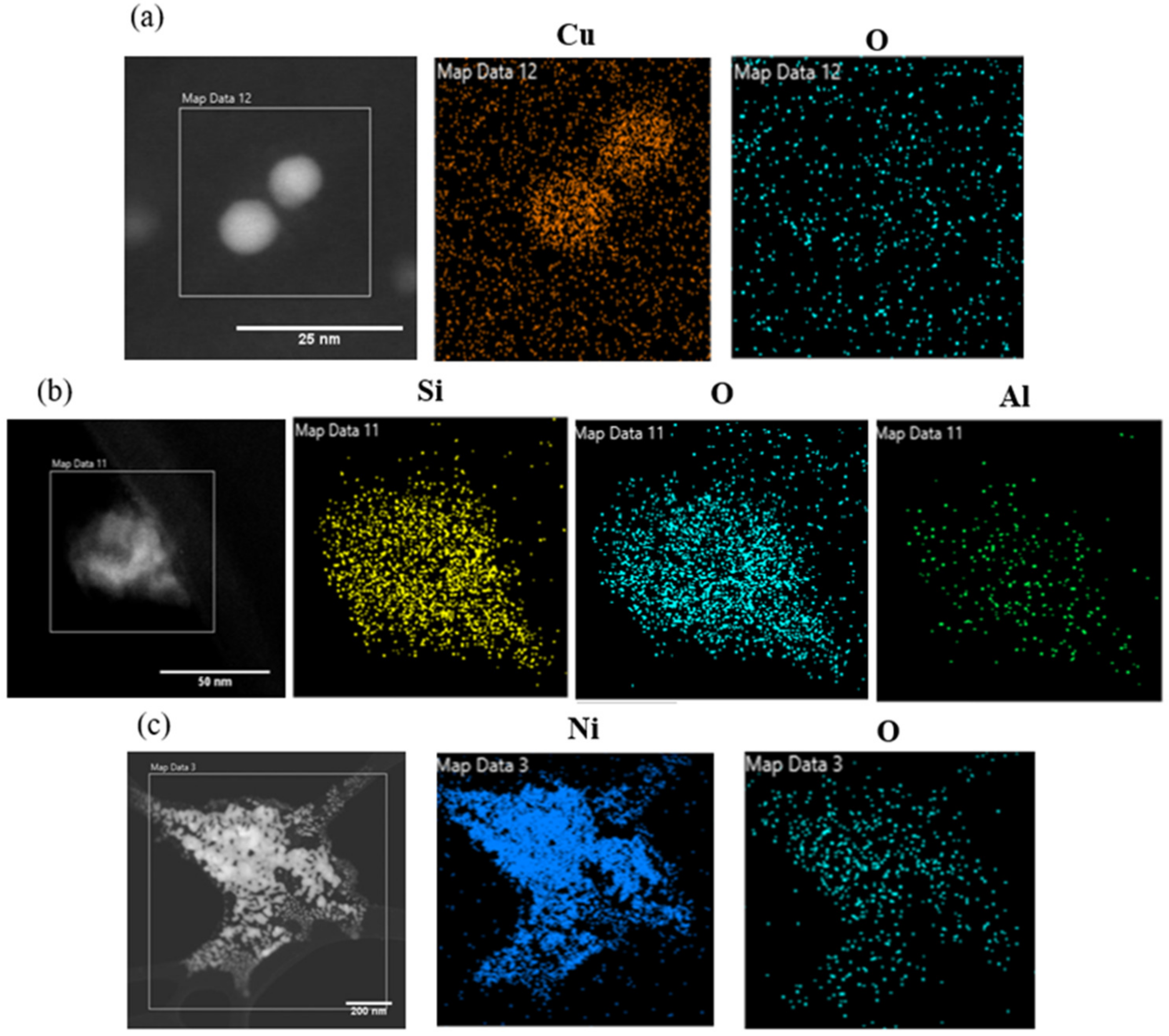
3.4. Morphology and Elemental Composition of Collected Airborne Particles within Breathing-Zone Filter Sample
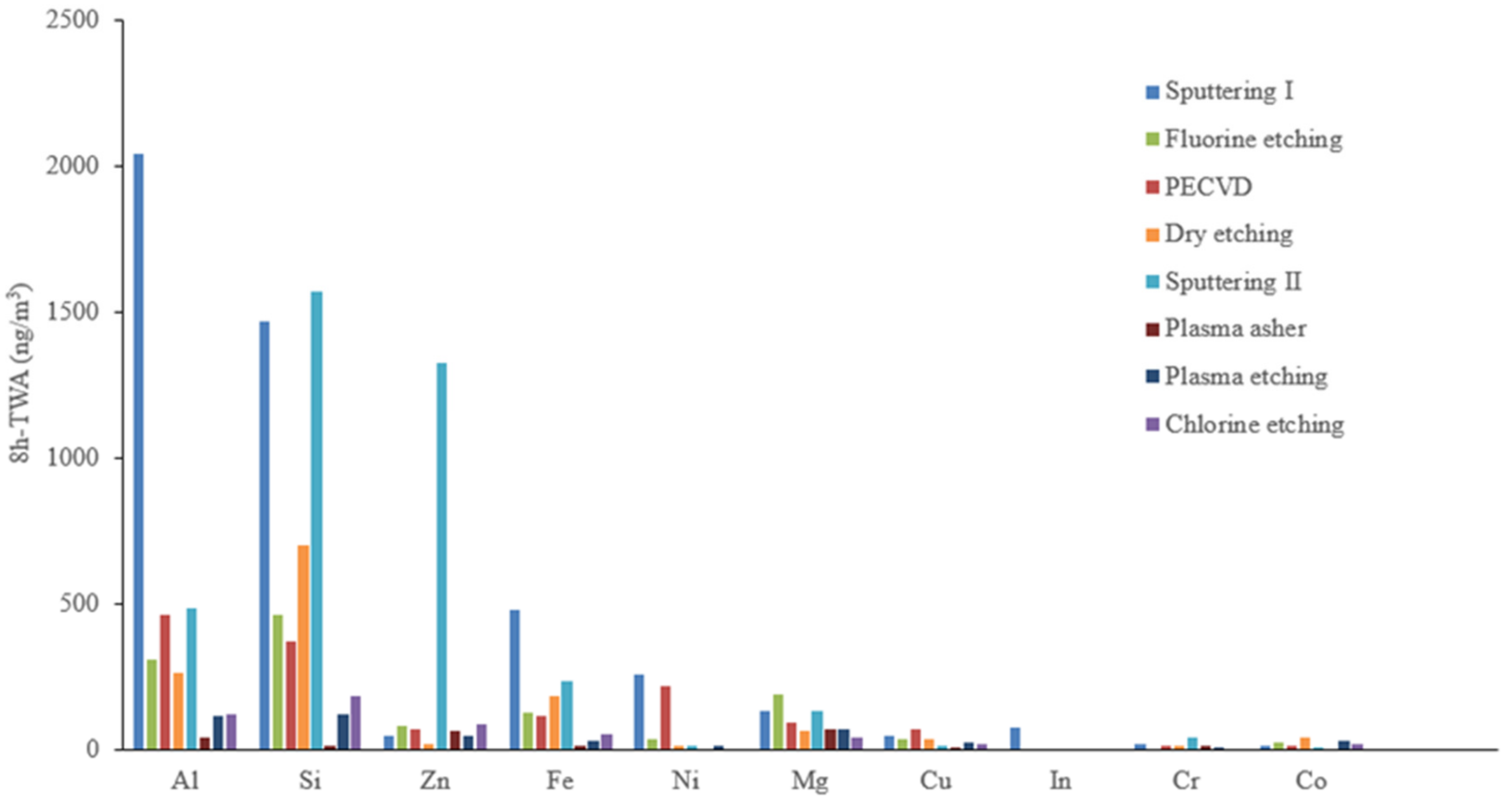
3.5. Mass Concentrations in Breathing Zone Area
3.6. Study Limitations
4. Conclusions
Supplementary Materials
Author Contributions
Funding
Institutional Review Board Statement
Informed Consent Statement
Data Availability Statement
Conflicts of Interest
References
- ISO 14633-1 2015; Cleanrooms and Associated Controlled Environments—Part 1: Classification of Air Cleanliness. ISO: Geneva, Switzerland, 1999.
- Choi, K. Airborne PM2.5 Characteristics in Semiconductor Manufacturing Facilities. AIMS Environ. Sci. 2018, 5, 216–228. [Google Scholar] [CrossRef]
- Speed, D.; Westerhoff, P.; Sierra-Alvarez, R.; Draper, R.; Pantano, P.; Aravamudhan, S.; Chen, K.L.; Hristovski, K.; Herckes, P.; Bi, X.; et al. Physical, Chemical, and in Vitro Toxicological Characterization of Nanoparticles in Chemical Mechanical Planarization Suspensions Used in the Semiconductor Industry: Towards Environmental Health and Safety Assessments. Environ. Sci. Nano 2015, 2, 227–244. [Google Scholar] [CrossRef]
- Dumitrescu, E.; Karunaratne, D.P.; Babu, S.V.; Wallace, K.N.; Andreescu, S. Interaction, Transformation and Toxicity Assessment of Particles and Additives Used in the Semiconducting Industry. Chemosphere 2018, 192, 178–185. [Google Scholar] [CrossRef] [PubMed]
- Zazzera, L.; Mader, B.; Ellefson, M.; Eldridge, J.; Loper, S.; Zabasajja, J.; Qian, J. Comparison of Ceria Nanoparticle Concentrations in Effluent from Chemical Mechanical Polishing of Silicon Dioxide. Environ. Sci. Technol. 2014, 48, 13427–13433. [Google Scholar] [CrossRef] [PubMed]
- Bocca, B.; Battistini, B.; Leso, V.; Fontana, L.; Caimi, S.; Fedele, M.; Iavicoli, I. Occupational Exposure to Metal Engineered Nanoparticles: A Human Biomonitoring Pilot Study Involving Italian Nanomaterial Workers. Toxics 2023, 11, 120. [Google Scholar] [CrossRef] [PubMed]
- Park, D.-U.; Zoh, K.E.; Jeong, E.K.; Koh, D.-H.; Lee, K.-H.; Lee, N.; Ha, K. Assessment of Occupational Health Risks for Maintenance Work in Fabrication Facilities: Brief Review and Recommendations. Saf. Health Work, 2023; in press. [Google Scholar] [CrossRef]
- Brenner, S.A.; Neu-Baker, N.M.; Caglayan, C.; Zurbenko, I.G. Occupational Exposure to Airborne Nanomaterials: An Assessment of Worker Exposure to Aerosolized Metal Oxide Nanoparticles in a Semiconductor Fab and Subfab. J. Occup. Environ. Hyg. 2016, 13, D138–D147. [Google Scholar] [CrossRef] [PubMed]
- Liao, B.X.; Tseng, N.C.; Li, Z.; Liu, Y.; Chen, J.K.; Tsai, C.J. Exposure Assessment of Process By-Product Nanoparticles Released during the Preventive Maintenance of Semiconductor Fabrication Facilities. J. Nanoparticle Res. 2018, 20, 203. [Google Scholar] [CrossRef]
- Shepard, M.N.; Brenner, S. An Occupational Exposure Assessment for Engineered Nanoparticles Used in Semiconductor Fabrication. Ann. Occup. Hyg. 2014, 58, 251–265. [Google Scholar] [CrossRef]
- Brenner, S.A.; Neu-Baker, N.M.; Eastlake, A.C.; Beaucham, C.C.; Geraci, C.L. NIOSH Field Studies Team Assessment: Worker Exposure to Aerosolized Metal Oxide Nanoparticles in a Semiconductor Fabrication Facility. J. Occup. Environ. Hyg. 2016, 13, 871–880. [Google Scholar] [CrossRef]
- Brenner, S.A.; Neu-Baker, N.M. Occupational Exposure to Nanomaterials: Assessing the Potential for Cutaneous Exposure to Metal Oxide Nanoparticles in a Semiconductor Facility. J. Chem. Health Saf. 2015, 22, 10–19. [Google Scholar] [CrossRef]
- Choi, K.-M.; Kim, J.H.; Park, J.H.; Kim, K.S.; Bae, G.N. Exposure Characteristics of Nanoparticles as Process By-Products for the Semiconductor Manufacturing Industry. J. Occup. Environ. Hyg. 2015, 12, D153–D160. [Google Scholar] [CrossRef] [PubMed]
- Choi, K.-M.; An, H.-C.; Kim, K.-S. Identifying the Hazard Characteristics of Powder Byproducts Generated from Semiconductor Fabrication Processes. J. Occup. Environ. Hyg. 2015, 12, 114–122. [Google Scholar] [CrossRef] [PubMed]
- Kim, E.A.; Lee, H.E.; Ryu, H.W.; Park, S.H.; Kang, S.K. Cases Series of Malignant Lymphohematopoietic Disorder in Korean Semiconductor Industry. Saf. Health Work 2011, 2, 122–134. [Google Scholar] [CrossRef]
- Kim, M.-H.; Kim, H.; Paek, D. The Health Impacts of Semiconductor Production: An Epidemiologic Review. Int. J. Occup. Environ. Health 2014, 20, 95–114. [Google Scholar] [CrossRef]
- Jiang, W.; Lin, S.; Chang, C.H.; Ji, Z.; Sun, B.; Wang, X.; Li, R.; Pon, N.; Xia, T.; Nel, A.E. Implications of the Differential Toxicological Effects of III-V Ionic and Particulate Materials for Hazard Assessment of Semiconductor Slurries. ACS Nano 2015, 9, 12011–12025. [Google Scholar] [CrossRef] [PubMed]
- Osborne, O.J.; Lin, S.; Jiang, W.; Chow, J.; Chang, C.H.; Ji, Z.; Yu, X.; Lin, S.; Xia, T.; Nel, A.E. Differential Effect of Micron-: Versus Nanoscale III-V Particulates and Ionic Species on the Zebrafish Gut. Environ. Sci. Nano 2017, 4, 1350–1364. [Google Scholar] [CrossRef]
- Qu, J.; Wang, J.; Zhang, H.; Wu, J.; Ma, X.; Wang, S.; Zang, Y.; Huang, Y.; Ma, Y.; Cao, Y.; et al. Toxicokinetics and Systematic Responses of Differently Sized Indium Tin Oxide (ITO) Particles in Mice via Oropharyngeal Aspiration Exposure. Environ. Pollut. 2021, 290, 117993. [Google Scholar] [CrossRef]
- Ham, S.; Yoon, C.; Kim, S.; Park, J.; Kwon, O.; Heo, J.; Park, D.; Choi, S.; Kim, S.; Ha, K.; et al. Arsenic Exposure during Preventive Maintenance of an Ion Implanter in a Semiconductor Manufacturing Factory. Aerosol Air Qual. Res. 2017, 17, 990–999. [Google Scholar] [CrossRef]
- Oberdörster, G.; Oberdörster, E.; Oberdörster, J. Nanotoxicology: An Emerging Discipline Evolving from Studies of Ultrafine Particles. Environ. Health Perspect. 2005, 113, 823–839. [Google Scholar] [CrossRef]
- Dankovic, D.A.; Kuempel, E.D. Current Intelligence Bulletin 63: Occupational Exposure to Titanium Dioxide. 2011, (NIOSH) 2011-160; pp. 1–140. Available online: https://stacks.cdc.gov/view/cdc/5922/cdc_5922_DS1.pdf (accessed on 9 May 2023).
- Howard, J. Current Intelligence Bulletin 65: Occupational Exposure to Carbon Nanotubes and Nanofibers. DHHS Public 2013, 2013, 145. [Google Scholar]
- Maher, B.A.; Ahmed, I.A.M.; Karloukovski, V.; MacLaren, D.A.; Foulds, P.G.; Allsop, D.; Mann, D.M.A.; Torres-Jardón, R.; Calderon-Garciduenas, L. Magnetite Pollution Nanoparticles in the Human Brain. Proc. Natl. Acad. Sci. USA 2016, 113, 10797–10801. [Google Scholar] [CrossRef] [PubMed]
- Prüst, M.; Meijer, J.; Westerink, R.H.S. The Plastic Brain: Neurotoxicity of Micro- and Nanoplastics. Part. Fibre Toxicol. 2020, 17, 24. [Google Scholar] [CrossRef] [PubMed]
- Singh, S. Zinc Oxide Nanoparticles Impacts: Cytotoxicity, Genotoxicity, Developmental Toxicity, and Neurotoxicity. Toxicol. Mech. Methods 2019, 29, 300–311. [Google Scholar] [CrossRef] [PubMed]
- Cary, C.; Stapleton, P. Determinants and Mechanisms of Inorganic Nanoparticle Translocation across Mammalian Biological Barriers. Arch. Toxicol. 2023, 97, 2111–2131. [Google Scholar] [CrossRef] [PubMed]
- Tröstl, J.; Tritscher, T.; Bischof, O.F.; Horn, H.G.; Krinke, T.; Baltensperger, U.; Gysel, M. Fast and Precise Measurement in the Sub-20nm Size Range Using a Scanning Mobility Particle Sizer. J. Aerosol Sci. 2015, 87, 75–87. [Google Scholar] [CrossRef]
- Stolzenburg, M.R.; McMurry, P.H. Method to Assess Performance of Scanning Mobility Particle Sizer (SMPS) Instruments and Software. Aerosol Sci. Technol. 2018, 52, 609–613. [Google Scholar] [CrossRef]
- CDC-NIOSH. Elements by ICP (Nitric/Perchloric Acid Ashing). NIOSH Man. Anal. Methods Method 2003, 7300, 1–8. [Google Scholar]
- CDC-NIOSH. Asbestos by TEM. NIOSH Man. Anal. Methods Method 1994, 7402, 94–113. [Google Scholar]
- Majestic, B.J.; Anbar, A.D.; Herckes, P. Elemental and Iron Isotopic Composition of Aerosols Collected in a Parking Structure. Sci. Total Environ. 2009, 407, 5104–5109. [Google Scholar] [CrossRef]
- Upadhyay, N.; Majestic, B.J.; Prapaipong, P.; Herckes, P. Evaluation of Polyurethane Foam, Polypropylene, Quartz Fiber, and Cellulose Substrates for Multi-Element Analysis of Atmospheric Particulate Matter by ICP-MS. Anal. Bioanal. Chem. 2009, 394, 255–266. [Google Scholar] [CrossRef]
- Kulmala, M.; Vehkamäki, H.; Petäjä, T.; Dal Maso, M.; Lauri, A.; Kerminen, V.M.; Birmili, W.; McMurry, P.H. Formation and Growth Rates of Ultrafine Atmospheric Particles: A Review of Observations. J. Aerosol Sci. 2004, 35, 143–176. [Google Scholar] [CrossRef]
- Occupational Chemical Database Home Page. Available online: https://www.osha.gov/chemicaldata/ (accessed on 9 May 2023).


| Sampling Equipment | Sampling Area | Nocturnal Background c (#/cm3) d | Working Hour e (#/cm3) | Maintenance Activity (#/cm3) | Maintenance Duration (min) | Maximum Value (#/cm3) |
|---|---|---|---|---|---|---|
| PECVD I a | MTW return air | 21 | 15 | 321 | 21 | 4120 |
| PECVD II | Nanofab | 7 | 313 | 476 | 90 | 11,800 |
| Plasma etching | MTW fab | 2 | 2 | 7 | 30 | 90 |
| Dry etching | MTW return air | 89 | 139 | 260 | 20 | 1380 |
| Fluorine etching | MTW return air | 54 | 16 | 523 | 12 | 1470 |
| Chlorine etching | MTW return air | 2 | 14 | 4 | 26 | 40 |
| Wet etching b | Nanofab | 15 | 201 | N/A | N/A | N/A |
| Sputtering I | MTW fab | 8 | 10 | 718 | 32 | 3440 |
| Sputtering II | MTW fab | 12 | 15 | 215 | 60 | 1380 |
| Plasma Asher | MTW fab | 14 | 23 | 16 | 30 | 54 |
Disclaimer/Publisher’s Note: The statements, opinions and data contained in all publications are solely those of the individual author(s) and contributor(s) and not of MDPI and/or the editor(s). MDPI and/or the editor(s) disclaim responsibility for any injury to people or property resulting from any ideas, methods, instructions or products referred to in the content. |
© 2024 by the authors. Licensee MDPI, Basel, Switzerland. This article is an open access article distributed under the terms and conditions of the Creative Commons Attribution (CC BY) license (https://creativecommons.org/licenses/by/4.0/).
Share and Cite
Zhang, Z.; Westerhoff, P.; Herckes, P. Evaluation of Potential Occupational Exposure and Release of Nanoparticles in Semiconductor-Manufacturing Environments. Atmosphere 2024, 15, 301. https://doi.org/10.3390/atmos15030301
Zhang Z, Westerhoff P, Herckes P. Evaluation of Potential Occupational Exposure and Release of Nanoparticles in Semiconductor-Manufacturing Environments. Atmosphere. 2024; 15(3):301. https://doi.org/10.3390/atmos15030301
Chicago/Turabian StyleZhang, Zhaobo, Paul Westerhoff, and Pierre Herckes. 2024. "Evaluation of Potential Occupational Exposure and Release of Nanoparticles in Semiconductor-Manufacturing Environments" Atmosphere 15, no. 3: 301. https://doi.org/10.3390/atmos15030301
APA StyleZhang, Z., Westerhoff, P., & Herckes, P. (2024). Evaluation of Potential Occupational Exposure and Release of Nanoparticles in Semiconductor-Manufacturing Environments. Atmosphere, 15(3), 301. https://doi.org/10.3390/atmos15030301