Communication

Experimental Investigation on the Electrical Properties of DPPT-TT Polymer Field-Effect Transistors Featuring Stair Gate Dielectric

College of Integrated Circuit Science and Engineering, Nanjing University of Posts and Telecommunications, Nanjing 210023, China
*
Authors to whom correspondence should be addressed.
Polymers 2025, 17(3), 289; https://doi.org/10.3390/polym17030289
Submission received: 31 December 2024 / Revised: 15 January 2025 / Accepted: 18 January 2025 / Published: 23 January 2025
(This article belongs to the Section Polymer Applications)

Abstract

:
P-type polymer field-effect transistors (PFETs) achieve wide applications due to their environmental compatibility and inherent flexibility. However, the dielectric in PFETs presents a vulnerability that restricts the development of the advancement of p-type power devices and power integrated circuits with high voltage in power devices. In this work, we provide a novel method that employs p-type polymer DPPT-TT high-voltage PFETs with a stair gate dielectric structure (SGD) at both the source and drain sides. The breakdown voltage of this device is significantly increased, rising from 19 V to 80 V. This improvement is attributable to the SGD structure’s ability to reduce the electric field between the source and drain. Although the step gate length (LSGD) is 50 μm, the on-state resistance only increases by 20% in comparison to conventional devices. The step region contributes an additional resistance of 2.5 × 10⁴ Ω/μm. The operational mechanism of the SGD PFET is demonstrated by TCAD simulations.

Graphical Abstract

1. Introduction

Significant advancements in polymer field-effect transistors over recent decades have broadened their applications across diverse domains, including flexible sensors, active-matrix organic-light-emitting diodes, biological monitoring, and solar energy conversion [1,2,3,4,5]. These devices are highly valued for their substantial functionality, tunable properties, mechanical robustness, and reliable performance even under stringent environmental conditions [6,7,8,9,10]. Moreover, the simplicity of their fabrication, large-area uniformity, and cost-effectiveness have propelled the development of PFET-based integrated circuits, encompassing analog, digital, and radio frequency identification circuits, to address the variegated demands of everyday life [11,12,13,14,15]. Consequently, the technology of PFETs is instrumental in the progress of advanced electronics. However, the current shortfall in high-performing organic semiconductor-based power devices represents a key obstacle in the development of fully flexible electronic systems.
Nevertheless, to date, there are few reports on the polymer-based power devices. For the conventional bottom-gate structure PFETs, the breakdown usually occurs in the gate dielectric in the overlap region between the gate and drain, which is the weak point under a high-operation voltage for thin-film transistors. Thus, the breakdown voltage is determined by the thickness of the dielectric [16]. Employing a thick gate dielectric can raise the BV, but it will greatly increase the on-state resistance (Ron) of the PFETs. An alternative approach involves implementing the drain-offset structure between the gate and the drain electrode to withstand the substantial voltage drop in high-voltage PFETs [17]. However, the offset region exhibits high resistance, leading to the degradation of the device’s Ron. Silicon-based power device technology presents challenges in its application to PFETs, primarily due to the complexities associated with doping processes and the limitations in utilizing photolithography processes [18,19,20]. For the same reason, the fabrication of PFETs with complex structures is also challenging.
In this work, we fabricated bottom-gate top-contact PFETs with the SGD positioned on both the source and drain sides. The semiconductor material is used diketopyrrolopyrrole-based polymer (DPPT-TT). The electrical properties include breakdown voltage (BV), threshold voltage (Vth), transconductance (gm), subthreshold swing (SS), and Ron. The SGD structure effectively reduced the electric field between the gate and drain, leading to the increase of BV. The channel region outside the SGD maintained a layer-thin gate dielectric, maintaining excellent output current capabilities. Consequently, the SGD PFETs with an LSGD of 50 μm achieved a BV of 84 V, which is more than four times that of conventional devices, while the Ron was 6.3 MΩ, only 1.3 times that of conventional devices. TCAD simulations were employed to provide an in-depth understanding of the operational mechanisms of SGD PFETs.

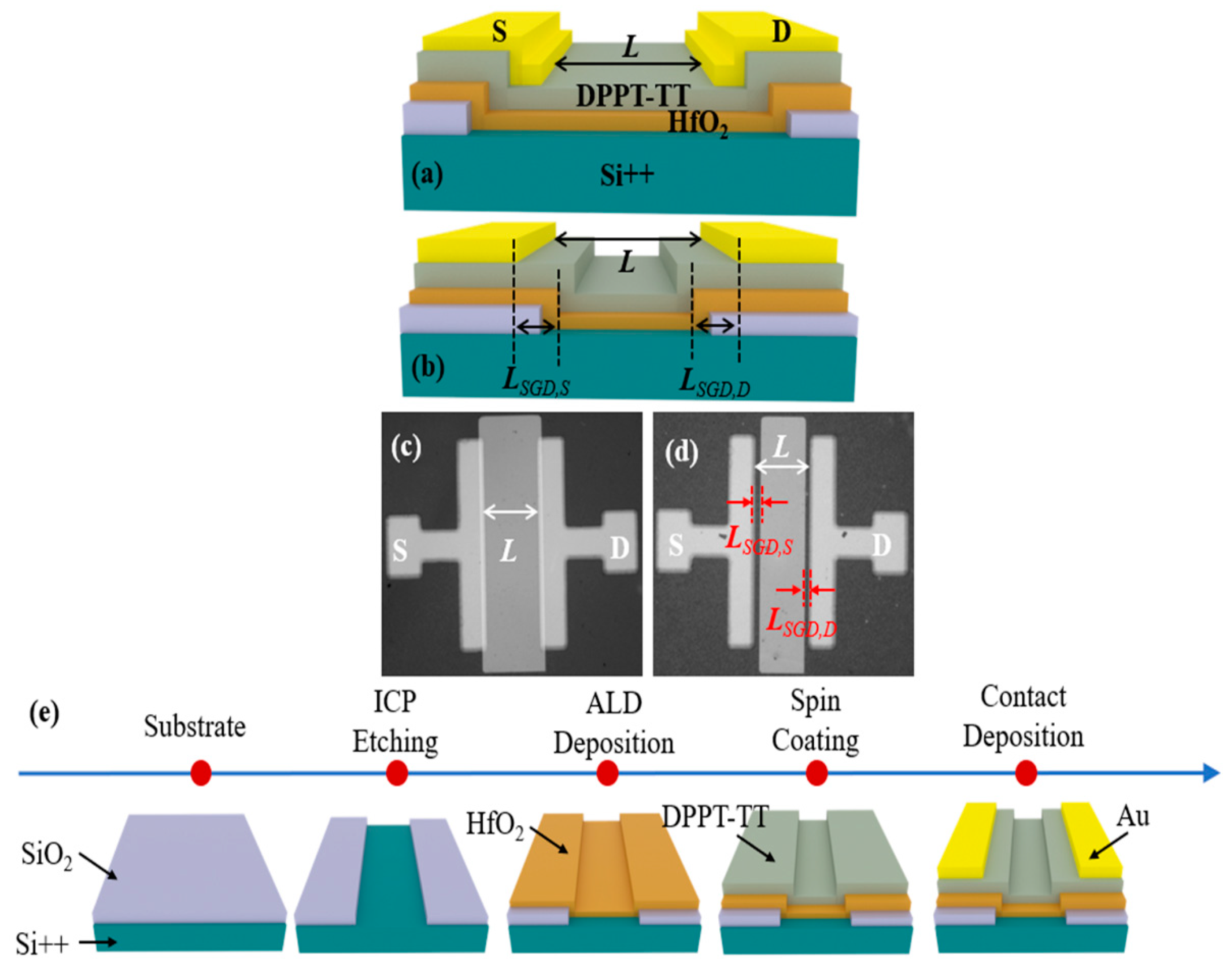
2. Experimental Section

A bottom-gate top-contact conventional polymer field-effect transistor (Conv. PFET) and the proposed 80-V SGD PFET are shown in Figure 1a,b, respectively. Figure 1c,d provides the optical images of the Conv. PFET and SGD PFET. The fabrication processes of SGD PFETs are shown in Figure 1e. The fabrication process began with a highly p-doped silicon wafer serving as the bottom gate, topped with a 50 nm thick layer of thermally grown silicon dioxide (SiO2) as the gate dielectric. The SiO2 was etched using an inductively coupled plasma etcher to create a trench. Subsequently, a 20 nm layer of hafnium dioxide (HfO2) was deposited via atomic layer deposition at 150 °C, forming the SGD structure combined with the SiO2. A 20 nm semiconductor layer of polymer DPPT-TT was then spin-coated onto the substrate and annealed at 150 °C for 1 h. Source–drain electrodes were formed by evaporating a 50 nm gold (Au) layer and patterning it with a hard mask. The SGD length (LSGD) is denoted as:
L S G D = L S G D , S + L S G D , D
where LSGD,S and LSGD,D are the stair length at the source and drain sides, respectively.
The SGD PFETs with LSGD of 50 μm (SGD-A), 100 μm (SGD-B), and 150 μm (SGD-C) were fabricated and investigated in this work. The key dimensions of the fabricated devices are shown in Table 1. All devices were fabricated with a channel length of 300 μm and a channel width of 1000 μm. The transfer and output characteristics of the PFETs were evaluated using a Keysight B1500 semiconductor precision analyzer. Essential parameters such as Vth, gm, and SS were derived from the transfer curves. The drain breakdown voltages were individually monitored. The operational principles of the investigated device were elucidated through TCAD simulations.

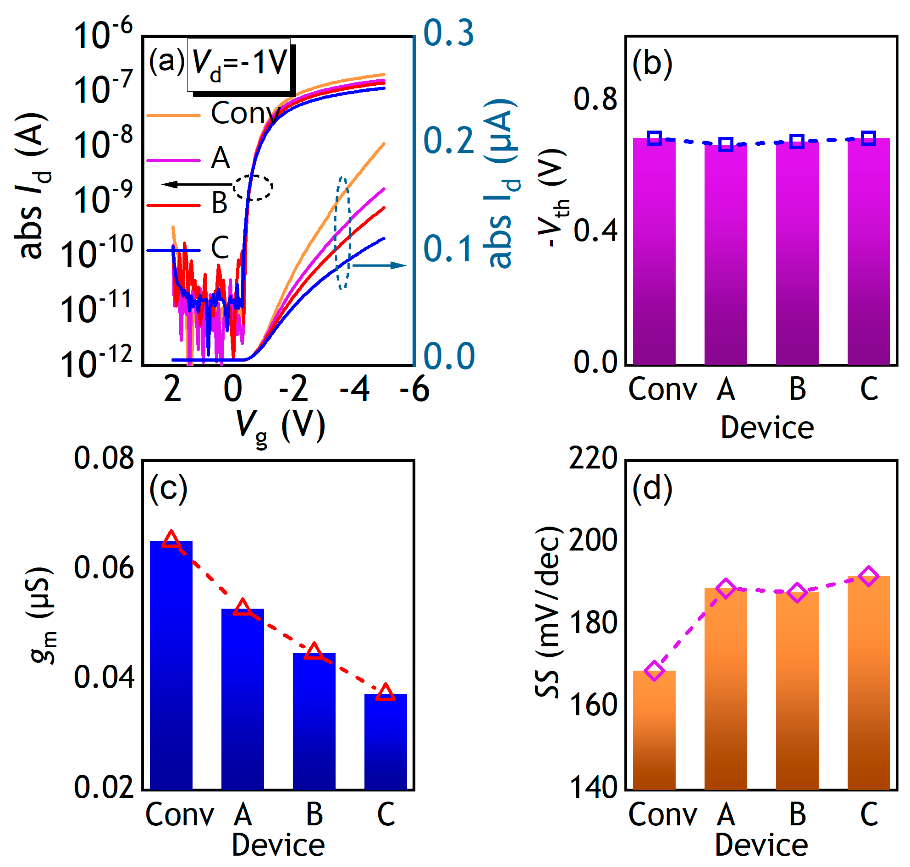
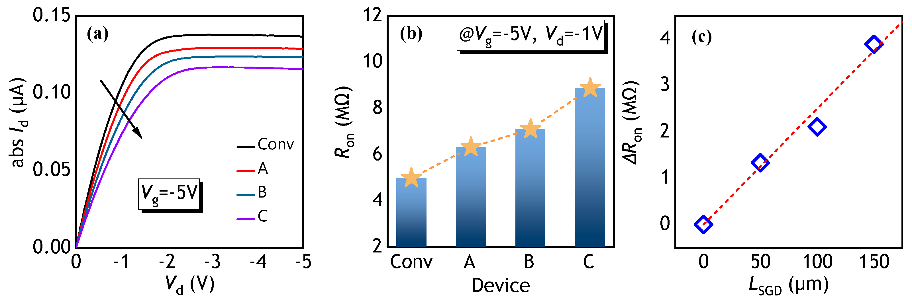
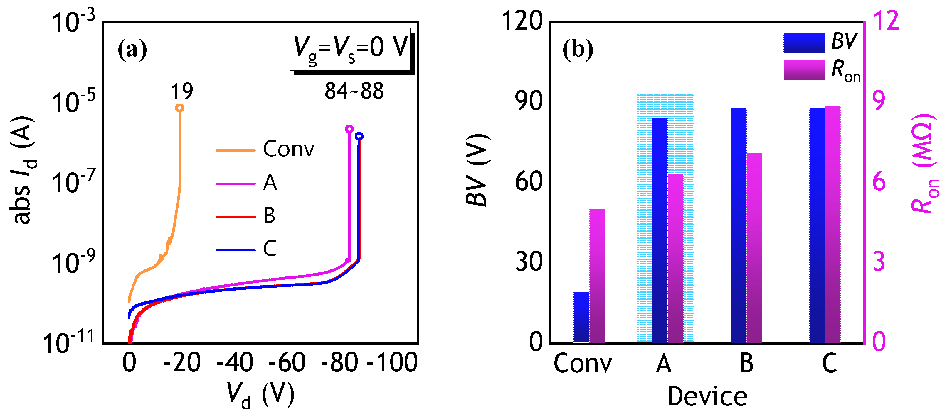
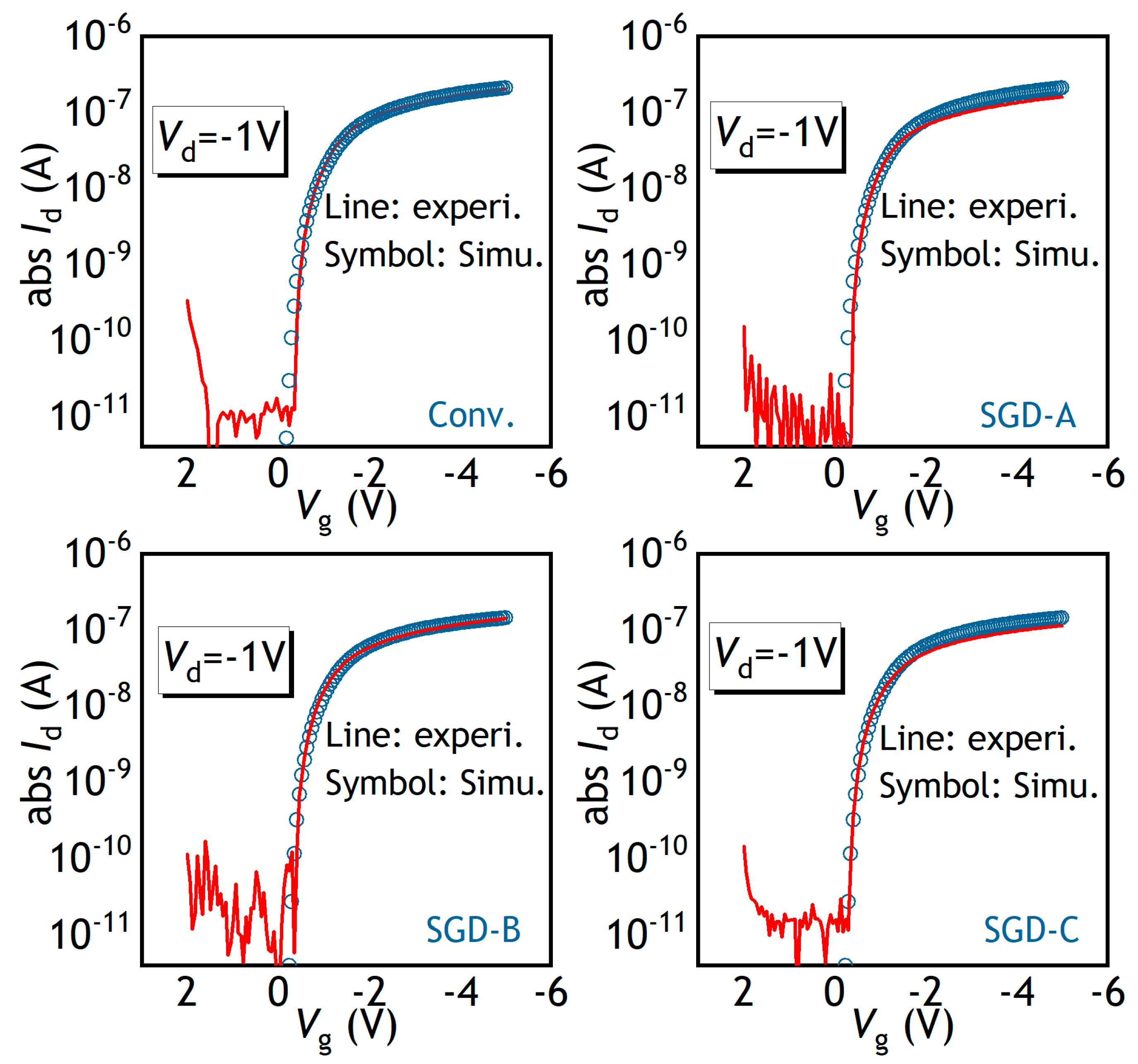
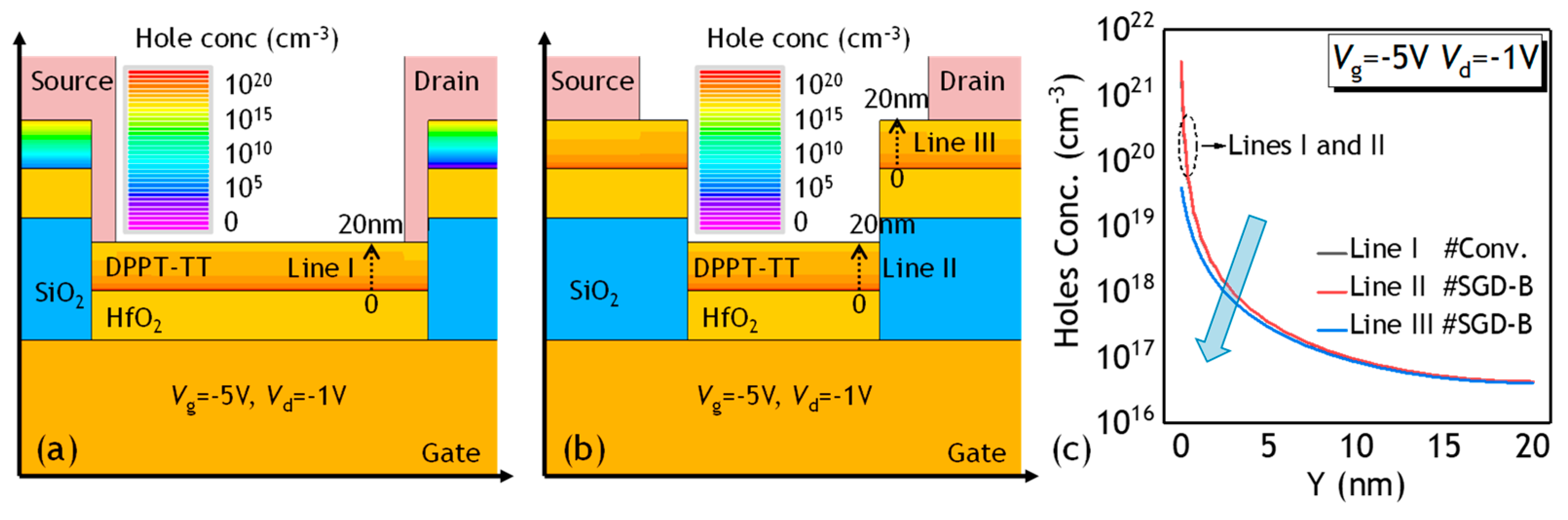
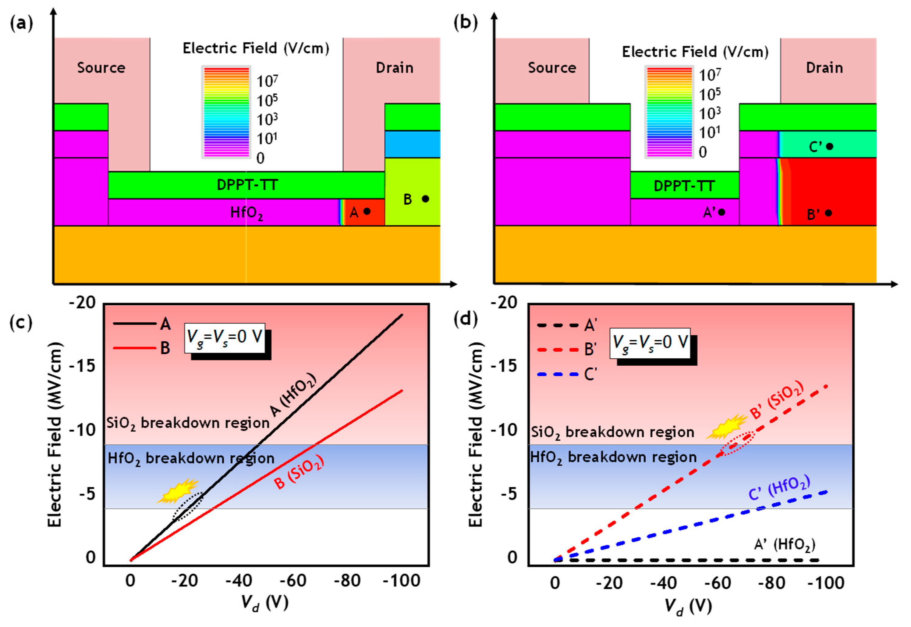
3. Results and Discussion

Figure 2a shows the transfer curves of the fabricated devices encompassing Conv., SGD-A, SGD-B, and SGD-C PFETs at the drain voltage (Vd) of −1 V. The extracted SS, Vth, and gm of the PFETs are delineated in Figure 2b–d. All devices exhibit a threshold voltage of around −0.7 V in Figure 2b, there is a characteristic that can be related to the 20 nm thin dielectric layer, which enhances gate control. The Vth of the Conv. PFETs and SGD PFETs with various LSGD are almost the same as each other. For the amorphous semiconductor-based channel material, the conduction threshold can be described as a transition of fermi level from deep to tail states [21]. The 50 nm SiO2 layer in the stair region increases the effective thickness of the gate dielectric (EOT), and EOT increases with the increasing LSGD. The weak reliance of the Vth on EOT means the fabricated OSC film has a low density of deep states. In addition, the increase in EOT contributes to a reduced gate capacitance of the SGD PFETs. Thus, the gm drops and decreases with the LGSD, as depicted in Figure 2c. Correspondingly, a little increase in SS for the SGD PFETs was caused by the decreasing gate capacitance, as shown in Figure 2d.
Figure 3a shows the output curves at the gate voltage (Vg) of −5 V for the Conv., SGD-A, SGD-B, and SGD-C PFETs. There is no current crowding at a low Vd for these PFETs. The decrease in Id for the increasing LSGD is noted. In the stair region of the SGD PFET, the gate dielectric thickness surpasses that of the Conv. PFET, resulting in a low electron concentration induced by the same Vg. The drop in carrier density elevates the resistance of the channel, intensifying with increasing LSGD, consequently diminishing the output current. Figure 3b illustrates Ron at the Vd of −1 V and Vg of −5 V in the linear region extracted from the transfer curves. When the LSGD increases, the Ron level exhibits an increasing trend. For SGD-A PFET with an LSGD of 50 μm, the Ron measures 6.3 MΩ, only 1.3 times the Ron of 5.0 MΩ of the Conv. PFET. The channel area outside the SGD region in the SGD-A PFET comprises a 20 nm thick HfO2 dielectric, maintaining a high concentration of the accumulated carriers and sustaining a low Ron. Figure 3c shows the ΔRon as the function of LGSD, extracted from Figure 3b. Extracting the on-state resistance from Figure 3b and plotting the change in on-state resistance separately, it can be observed that the increase in conduction resistance caused by the SGD structure exhibits a nearly linear relationship of a slope of 2.5 × 10⁴ Ω/μm. This indicates that the SGD structure does not have a particularly significant impact on the on-state resistance.
The breakdown characteristics of the proposed PFETs are examined. The Id-Vd curves at both the Vg and the source voltage of 0 V are presented in Figure 4a. The breakdown occurs in a hard breakdown mode, which is irreversible. Furthermore, the extracted BV and Ron of the studied PFETs are depicted in Figure 4b. Conv. PFETs, with only a 20 nm thick HfO2 between the gate and drain, exhibit the lowest breakdown voltage of 19 V. In contrast, PFETs with the SGD structure, which combines a 50nm SiO2 layer with a 20 nm HfO2 in the overlap region, see a significant increase in breakdown voltage. In an ideal situation, the electric displacement vector is continuous at the interface between different dielectric layers. When a drain voltage is applied, the electric field in the dielectric layer with a higher dielectric constant (HfO2) is lower than that in the dielectric layer with a low dielectric constant (SiO2). When the thickness of SiO2 is higher than that of HfO2, most electric field is endured by the SiO2, leading to a higher breakdown voltage. All SGD PFETs achieve similar BV values due to the constant SGD thickness in the stair region of these devices. The SGD-A PFET stands out with a Ron of 6.3 MΩ and a BV of 84 V, exhibiting superior HV performance compared to its counterparts.
The experimental findings indicate that the SGD PFET can achieve a favorable trade-off between Ron and BV. To gain deeper insights into the operational mechanisms of the SGD PFETs, simulations using TCAD_Silvaco were undertaken. Table 2 summarizes the material simulation parameters for the OSC-based semiconductor, encompassing the energy band gap, electron affinity, effective density of states in the highest occupied molecular orbital (HOMO) and lowest unoccupied molecular orbital (LUMO), as well as the gate dielectric permittivity and contact work function.
The subgap density of states (DOS) model, comprising four parameterized components—namely, the acceptor-like exponential function, the acceptor-like Gaussian function, the donor-like exponential function, and the donor-like Gaussian function—proves instrumental in characterizing trap DOS within the bulk OSC-based channel material. In the case of OSC materials, exponential DOS is applied to represent tail states close to the conduction band edge and valence band edge, whereas Gaussian DOS functions are employed to characterize deep gap states.
Considering that the PFETs operate in p-type mode, we considered mainly the donor-like states in simulation. The donor-like exponential DOS is depicted by [22]:
g T D E = N T D exp E H O M O E W T D
where EHOMO is the energy level of HOMO and E is the energy level. NTD is the donor-type intercept DOS at EHOMO, and WTD is the characteristic decay energy. The donor-like Gaussian DOS is given by:
g G D E = N G D e x p E E G D W G D 2
where NGD is the trap density at the central energy EGD of the Gaussian distribution, and WGD is the characteristic decay energy. The essential fitting parameters of the DOS model are detailed in Table 3.
Figure 5 shows the comparison between the transfer characteristics of experimental data and simulated results about SGD-A, SGD-B, and SGD-C PFETs. The simulations exhibit a satisfactory alignment with the experimental data.
Figure 6 depicts the simulated distribution of hole concentration in the DPPT-TT material within both the Conv. PFET and SGD-B PFET at the Vg of −5 V and Vd of −1 V. The hole concentration profiles along lines I in the channel of the Conv. PFET, as well as along lines II and III in the channel of the SGD-B PFET, are presented in Figure 6c. For the SGD-B PFET, the carrier concentration along line III appears lower than that along line II, indicating reduced channel carrier density in the stair region compared to regions outside the stair region. The diminished capacitance of the thick SGD featuring a bilayer gate dielectric results in decreased gate-induced carriers within the stair channel region, thereby elevating channel resistance. Consequently, the output current of the SGD PFET falls below that of the Conv. PFET. It is significant to observe that lines I and II exhibit identical carrier distributions. Specifically, the gate dielectric beneath the active layer beyond the stair region consists of a 20 nm HfO2 layer, mirroring the setup in the Conv. PFET. Under the same Vg, the induced holes in the channel region with the singular dielectric are on the same level as that of Conv. PFET. The channel outside the stair region with a high carrier concentration, ensures the low sacrifice in current for the power SGD PFET.
Figure 7a,b show the simulation results illustrating the distribution of electric fields at the Vg = Vs = 0 V and Vd = 100 V within the dielectric for the Conv. PFET and SGD-B PFET, respectively. The electric field, varying with Vd at positions A and B in the Conv. PFET and A’, B’, and C’ in SGD-B PFET, are shown in Figure 7c,d correspondingly. In the Conv. PFET, the electric field at position A within the HfO2 surpasses that at position B within the SiO2 and reaches a peak of 4 MV/cm at the Vd of −20 V, nearing the critical electric field of HfO2, resulting in a limited BV. Conversely, in the SGD-B PFET, the SGD structure diminishes the electric field at position A’ within the HfO2, identified as a vulnerable point in Conv. PFETs when operating at high Vd, by optimizing the distribution of electric fields. Positions A’ and C’ experience subdued electric fields at elevated Vd levels. The electric field at position B’ in the stair region, featuring a thicker total gate dielectric, absorbs the majority of the electric field at higher Vd, thereby elevating the BV.
The developed SGD PFETs significantly raise the BV and can reduce Ron by reducing the LSGD, showcasing the substantial potential for application in power management circuits.

4. Conclusions

In this study, we introduce a novel approach involving p-type high-voltage PFETs that incorporate an SGD structure at both the source and drain terminals. The polymer DPPT-TT was deposited via spin-coating onto the SGD consisting of HfO2 and SiO2 layers to fabricate power SGD PFETs. Notably, the BV of the proposed device was elevated from 19 V to over 80 V. The SGD structure effectively reduces the electric field between the drain and gate, thereby enhancing the BV. With an SGD length of 50 μm, the Ron only experienced a modest 20% decline compared to conventional devices. Through TCAD simulation, the operational principles of the SGD PFETs were elucidated. This approach allows for the simultaneous achievement of high BV and low Ron in power PFETs.

Author Contributions

Conceptualization, H.Z. and Y.Q.; methodology, H.Z.; software, Y.Q.; validation, H.Z., Y.Q. and Q.C.; formal analysis, H.Z.; investigation, Y.Q.; resources, Y.Q.; data curation, H.Z. and Y.Q.; writing—original draft preparation, H.Z. and Y.Q.; writing—review and editing, Y.Y., Q.C. and L.C.; visualization, H.S.; supervision, Y.X. and G.Y.; project administration, Y.X. and G.Y.; funding acquisition, G.Y. All authors have read and agreed to the published version of the manuscript.

Funding

This work was supported by Natural Science Research Start-up Foundation of Recruiting Talents of Nanjing University of Posts and Telecommunications under Grant NY223159 and National Natural Science Foundation of China under Grant 62404110.

Data Availability Statement

The original contributions presented in this study are included in the article. Further inquiries can be directed to the corresponding authors.

Conflicts of Interest

The authors declare no conflicts of interest.

References

  1. Harikesh, P.C.; Yang, C.-Y.; Tu, D.; Gerasimov, J.Y.; Dar, A.M.; Armada-Moreira, A.; Massetti, M.; Kroon, R.; Bliman, D.; Olsson, R.; et al. Organic electrochemical neurons and synapses with ion mediated spiking. Nat. Commun. 2022, 13, 901. [Google Scholar] [CrossRef] [PubMed]
  2. Su, Y.; Geng, D.; Chen, Q.; Ji, H.; Li, M.; Shang, G.; Liu, L.; Duan, X.; Chuai, X.; Huang, S.; et al. Novel TFT-Based emission driver in high performance AMOLED display applications. Org. Electron. 2021, 93, 106160. [Google Scholar] [CrossRef]
  3. Petritz, A.; Karner-Petritz, E.; Uemura, T.; Schäffner, P.; Araki, T.; Stadlober, B.; Sekitani, T. Imperceptible energy harvesting device and biomedical sensor based on ultraflexible ferroelectric transducers and organic diodes. Nat. Commun. 2021, 12, 2399. [Google Scholar] [CrossRef] [PubMed]
  4. Wu, Z.; Yin, H.; Li, G.; Ji, Z. Recent progress in semitransparent organic solar cells. Org. Electron. 2024, 129, 107060. [Google Scholar] [CrossRef]
  5. Shiwaku, R.; Matsui, H.; Nagamine, K.; Uematsu, M.; Mano, T.; Maruyama, Y.; Nomura, A.; Tsuchiya, K.; Hayasaka, K.; Takeda, Y.; et al. A Printed Organic Circuit System for Wearable Amperometric Electrochemical Sensors. Sci. Rep. 2018, 8, 6368. [Google Scholar] [CrossRef] [PubMed]
  6. Wu, W.; Geng, D.; Chen, C.; Chuai, X.; Li, S.; Lu, N.; Li, L. High-speed, low-voltage, small-pitch and robust OTFT-based integrated gate driver for active-matrix displays. Org. Electron. 2024, 124, 106939. [Google Scholar] [CrossRef]
  7. Li, M.; Zheng, J.; Wang, X.; Yu, R.; Wang, Y.; Qiu, Y.; Cheng, X.; Wang, G.; Chen, G.; Xie, K.; et al. Light-responsive self-strained organic semiconductor for large flexible OFET sensing array. Nat. Commun. 2022, 13, 4912. [Google Scholar] [CrossRef] [PubMed]
  8. Chen, X.; Wang, Z.; Qi, J.; Hu, Y.; Huang, Y.; Sun, S.; Sun, Y.; Gong, W.; Luo, L.; Zhang, L.; et al. Balancing the film strain of organic semiconductors for ultrastable organic transistors with a five-year lifetime. Nat. Commun. 2022, 13, 1480. [Google Scholar] [CrossRef] [PubMed]
  9. Bharti, D.; Raghuwanshi, V.; Varun, I.; Mahato, A.K.; Tiwari, S.P. High Performance and Electro-Mechanical Stability in Small Molecule: Polymer Blend Flexible Organic Field-Effect Transistors. IEEE Electron. Device Lett. 2016, 37, 1215–1218. [Google Scholar] [CrossRef]
  10. Knopfmacher, O.; Hammock, M.L.; Appleton, A.L.; Schwartz, G.; Mei, J.; Lei, T.; Pei, J.; Bao, Z. Highly stable organic polymer field-effect transistor sensor for selective detection in the marine environment. Nat. Commun. 2014, 5, 2954. [Google Scholar] [CrossRef] [PubMed]
  11. Bilgaiyan, A.; Cho, S.-I.; Abiko, M.; Watanabe, K.; Mizukami, M. Flexible, high mobility short-channel organic thin film transistors and logic circuits based on 4H–21DNTT. Sci. Rep. 2021, 11, 11710. [Google Scholar] [CrossRef] [PubMed]
  12. Luo, Z.; Peng, B.; Zeng, J.; Yu, Z.; Zhao, Y.; Xie, J.; Lan, R.; Ma, Z.; Pan, L.; Cao, K.; et al. Sub-thermionic, ultra-high-gain organic transistors and circuits. Nat. Commun. 2021, 12, 1928. [Google Scholar] [CrossRef] [PubMed]
  13. Ogier, S.D.; Matsui, H.; Feng, L.; Simms, M.; Mashayekhi, M.; Carrabina, J.; Terés, L.; Tokito, S. Uniform, high performance, solution processed organic thin-film transistors integrated in 1 MHz frequency ring oscillators. Org. Electron. 2018, 54, 40–47. [Google Scholar] [CrossRef]
  14. Kjellander, B.K.C.; Smaal, W.T.T.; Myny, K.; Genoe, J.; Dehaene, W.; Heremans, P.; Gelinck, G.H. Optimized circuit design for flexible 8-bit RFID transponders with active layer of ink-jet printed small molecule semiconductors. Org. Electron. 2013, 14, 768–774. [Google Scholar] [CrossRef]
  15. Ran, W.; Ren, Z.; Wang, P.; Yan, Y.; Zhao, K.; Li, L.; Li, Z.; Wang, L.; Yang, J.; Wei, Z.; et al. Integrated polarization-sensitive amplification system for digital information transmission. Nat. Commun. 2021, 12, 6476. [Google Scholar] [CrossRef] [PubMed]
  16. Romanuik, S.F.; Rout, B.; Girard-Lauriault, P.-L.; Bhadra, S. Resolving Unusual Gate Current and Dielectric Breakdown of Solution Processed Carbon Nanotube Thin Film Transistor. In Proceedings of the 2022 IEEE International Symposium on Circuits and Systems (ISCAS), Austin, TX, USA, 27 May–1 June 2022; pp. 2008–2011. [Google Scholar]
  17. Zhang, J.; Zhou, J.; Wang, Y.; Li, M.; Du, L.; Chen, J.; Zhang, M.; Yao, J.; Zhang, G.; Sun, H.; et al. A 2.2kV Organic Semiconductor- Based Lateral Power Device. IEEE Electron. Device Lett. 2022, 43, 276–279. [Google Scholar] [CrossRef]
  18. Huseynova, G.; Xu, Y.; Nketia Yawson, B.; Shin, E.-Y.; Lee, M.J.; Noh, Y.-Y. P-type doped ambipolar polymer transistors by direct charge transfer from a cationic organic dye Pyronin B ferric chloride. Org. Electron. 2016, 39, 229–235. [Google Scholar] [CrossRef]
  19. Lüssem, B.; Keum, C.-M.; Kasemann, D.; Naab, B.; Bao, Z.; Leo, K. Doped Organic Transistors. Chem. Rev. 2016, 116, 13714–13751. [Google Scholar] [CrossRef] [PubMed]
  20. Jang, J.; Song, Y.; Yoo, D.; Kim, T.-Y.; Jung, S.-H.; Hong, S.; Lee, J.-K.; Lee, T. Micro-scale twistable organic field effect transistors and complementary inverters fabricated by orthogonal photolithography on flexible polyimide substrate. Org. Electron. 2014, 15, 2822–2829. [Google Scholar] [CrossRef]
  21. Lee, S.; Nathan, A. Conduction Threshold in Accumulation-Mode InGaZnO Thin Film Transistors. Sci. Rep. 2016, 6, 22567. [Google Scholar] [CrossRef] [PubMed]
  22. Silvaco International. Atlas User’s Manual; Silvaco International: Santa Clara, CA, USA, 2019; pp. 1–1797. [Google Scholar]
Figure 1. Schematic views of the (a) Conv. PFET and (b) SGD PFET. Optical images of the (c) Conv. PFET and (d) SGD PFET. (e) The fabrication process flow of the SGD PFETs.
Polymers 17 00289 g001
Figure 2. (a) Transfer curves of the conventional, SGD-A, SGD-B, and SGD-C PFETs. (b) Vth, (c) gm, and (d) SS versus the studied PFETs.
Polymers 17 00289 g002
Figure 3. (a) Output curves of the conventional, SGD-A, SGD-B, and SGD-C PFETs at the Vg of −5 V. (b) Extracted Ron in the linear region and (c) ΔRon versus LGSD for the studied PFETs.
Polymers 17 00289 g003
Figure 4. (a) Id versus the Vd for the conventional, SGD-A, SGD-B, and SGD-C PFETs. The breakdown was measured by sweeping the Vd with the Vg and vs. grounded. (b) The obtained BV and Ron of the PFETs.
Polymers 17 00289 g004
Figure 5. TCAD simulation fitting results for the transfer curves of conventional, SGD-A, SGD-B, and SGD-C PFETs at Vd of −1 V, respectively.
Polymers 17 00289 g005
Figure 6. Simulated results on the hole concentration distribution of (a) Conv. PFET, and (b) SGD-B PFET with the LSGD of 100 μm. (c) Hole concentration along lines I-III.
Polymers 17 00289 g006
Figure 7. Simulated results on the electric field distribution in the dielectric of (a) Conv. PFET, and (b) SGD-B PFET with the LSGD of 100 μm at the Vg = Vs = 0 V, Vd = −100 V. The electric field at randomly selected points in the gate and drain overlap region. Electric field versus Vd at positions (c) A, B in Conv. PFET, (d) A’ B’, and C’ in SGB-B PFET. The blue area is the breakdown region of HfO2, and the red area is the breakdown region of SiO2.
Polymers 17 00289 g007
Table 1. Key dimensions of the fabricated devices.
DeviceConvABC
tHfO2 (nm)20202020
tSiO2 (nm)/505050
LSGD (μm)/50100150
Table 2. Key simulation parameters of the material.
Energy band gap (eV) 1.26
Electron affinity (eV)4.07
Effective density of states (HOMO) (cm−3)1.0 × 10²¹
Effective density of states (LUMO) (cm−3)1.0 × 10²¹
Permittivity of HfO221
Permittivity of SiO23.9
Work function of contacts (eV)5.1
Table 3. Key simulation parameters of the bulk defects model.
NTD (cm−3eV−1)WTD (eV)NGD (cm−3eV−1)WGD (eV)EGD (eV)
1.0 × 10180.11.0 × 10160.10.4
Disclaimer/Publisher’s Note: The statements, opinions and data contained in all publications are solely those of the individual author(s) and contributor(s) and not of MDPI and/or the editor(s). MDPI and/or the editor(s) disclaim responsibility for any injury to people or property resulting from any ideas, methods, instructions or products referred to in the content.

