
Bio-Based Polymeric Substrates for Printed Hybrid Electronics


Abstract
:1. Introduction
2. Materials and Methods
2.1. Materials
2.2. Cast Film Extrusion
2.3. Orientation and Annealing
2.4. Thermal Analysis
2.5. Tensile Properties
2.6. Screen-Printing of Silver
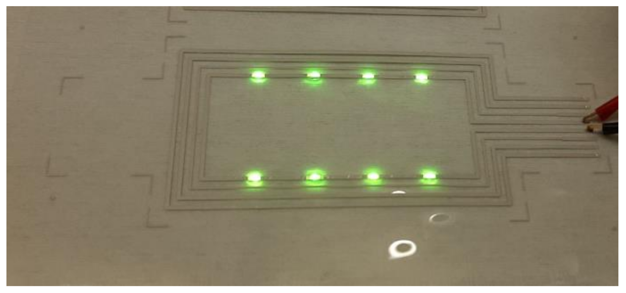
2.7. Hybrid-Integration of LEDs
2.8. Film Characterisation
2.9. Scanning Electron Microscopy (SEM)
3. Results and Discussion
3.1. Thermal Properties and Crystallinity
3.2. Tensile Properties
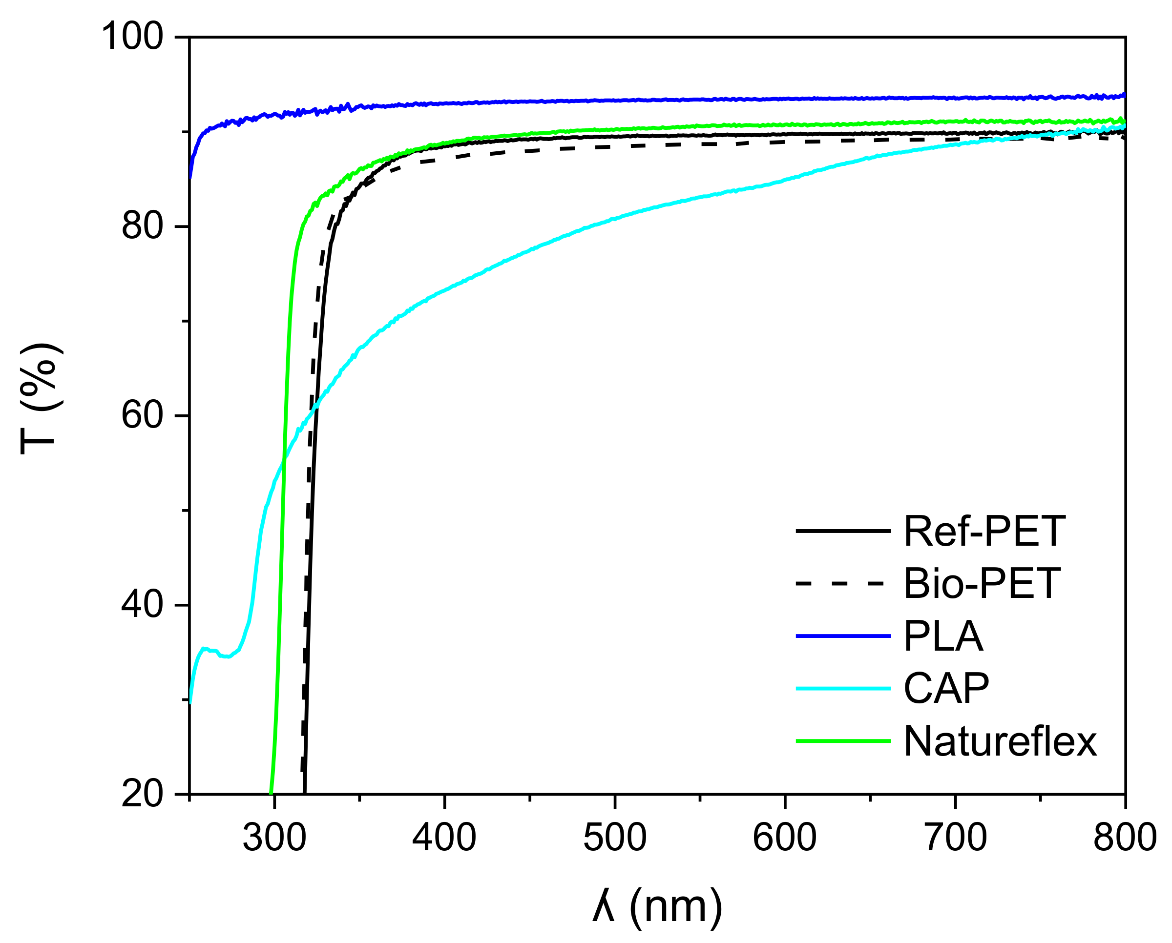
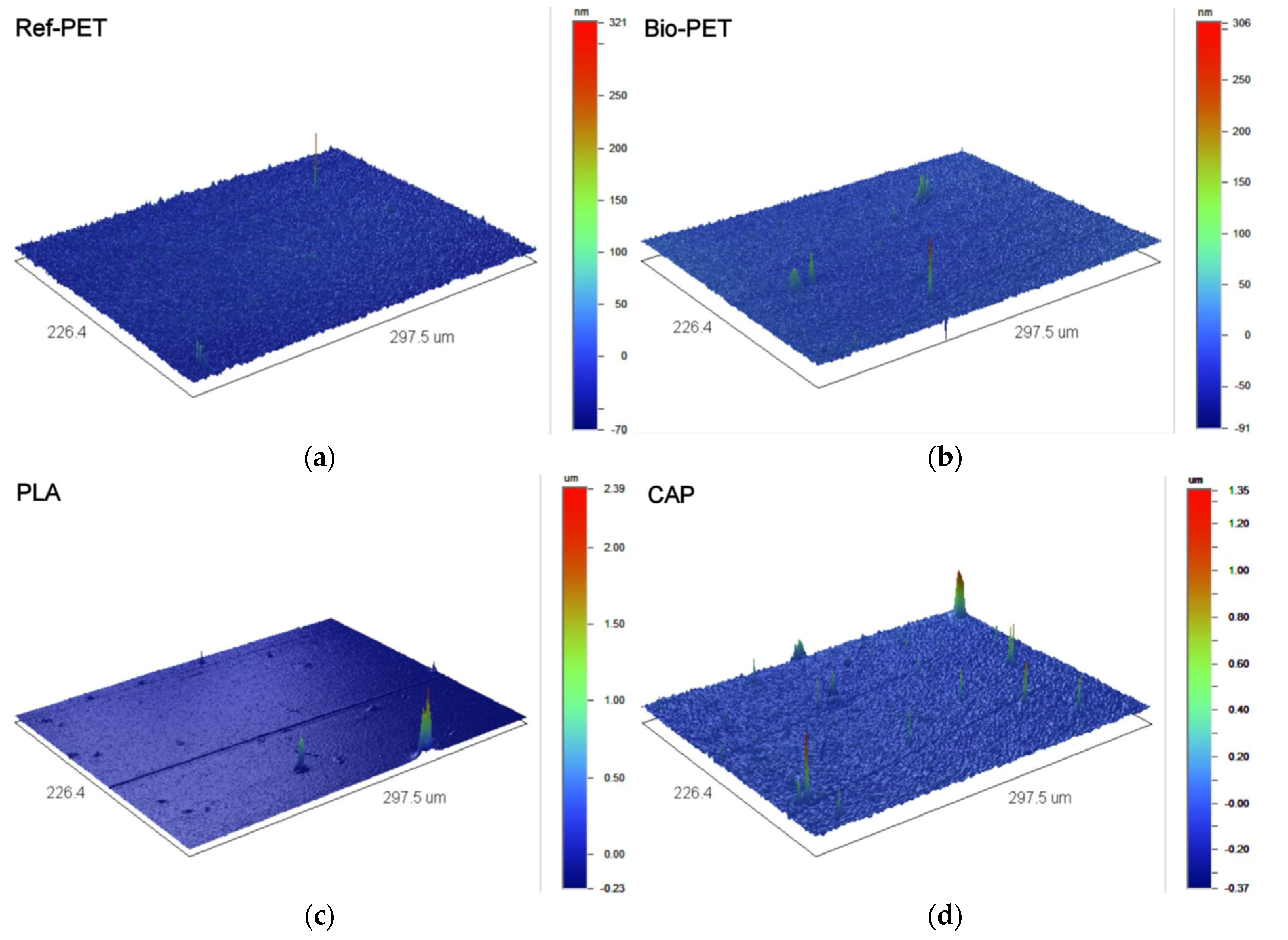
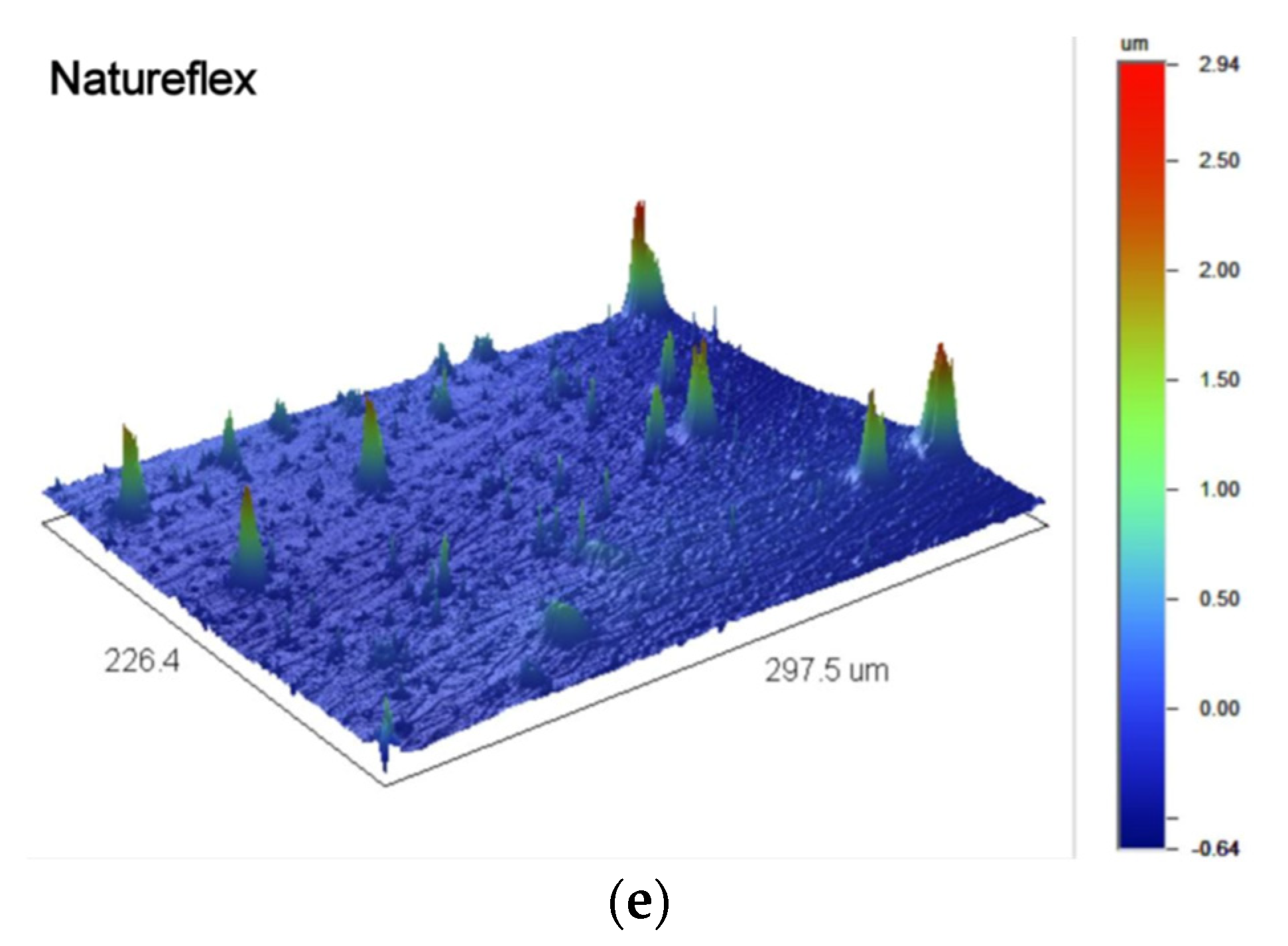
3.3. Transparency and Surface Properties
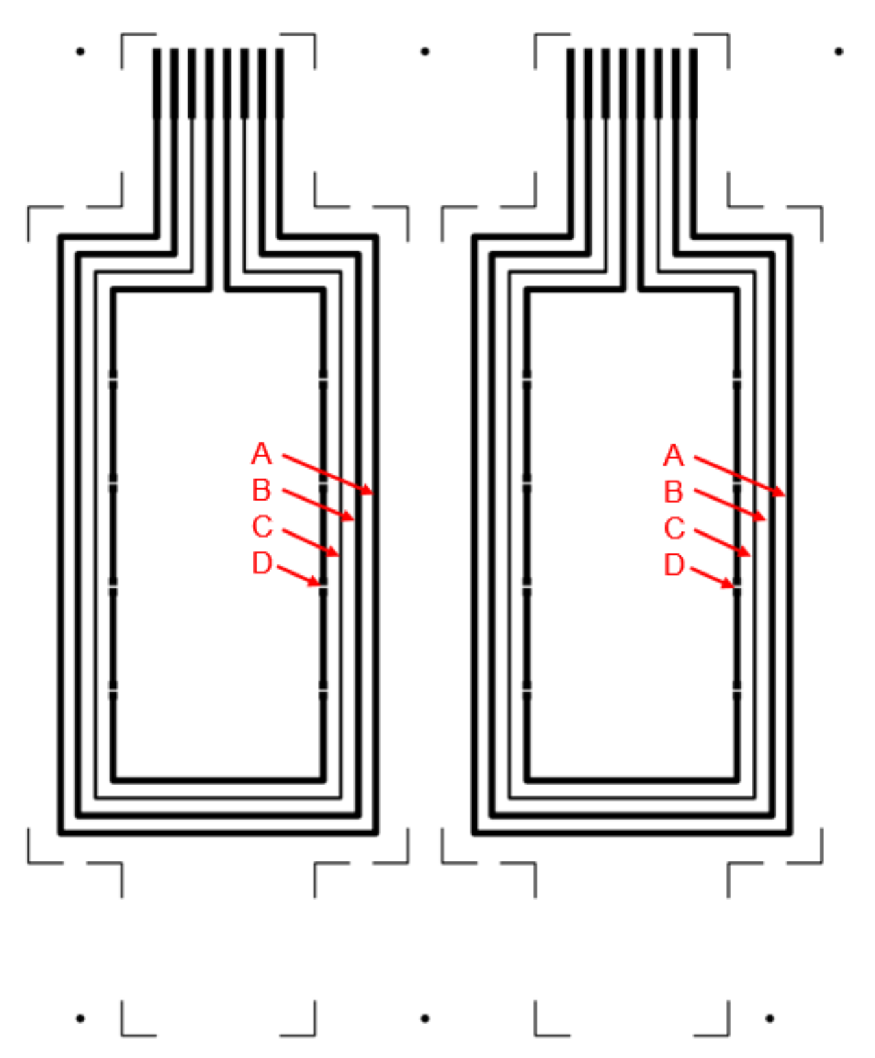
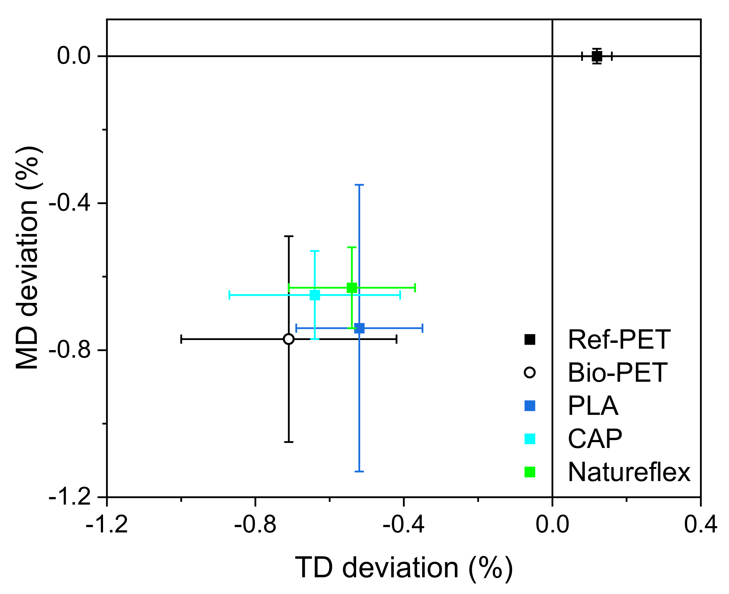
3.4. Dimensional Stability and Resistance of S2S Screen-Printed Films
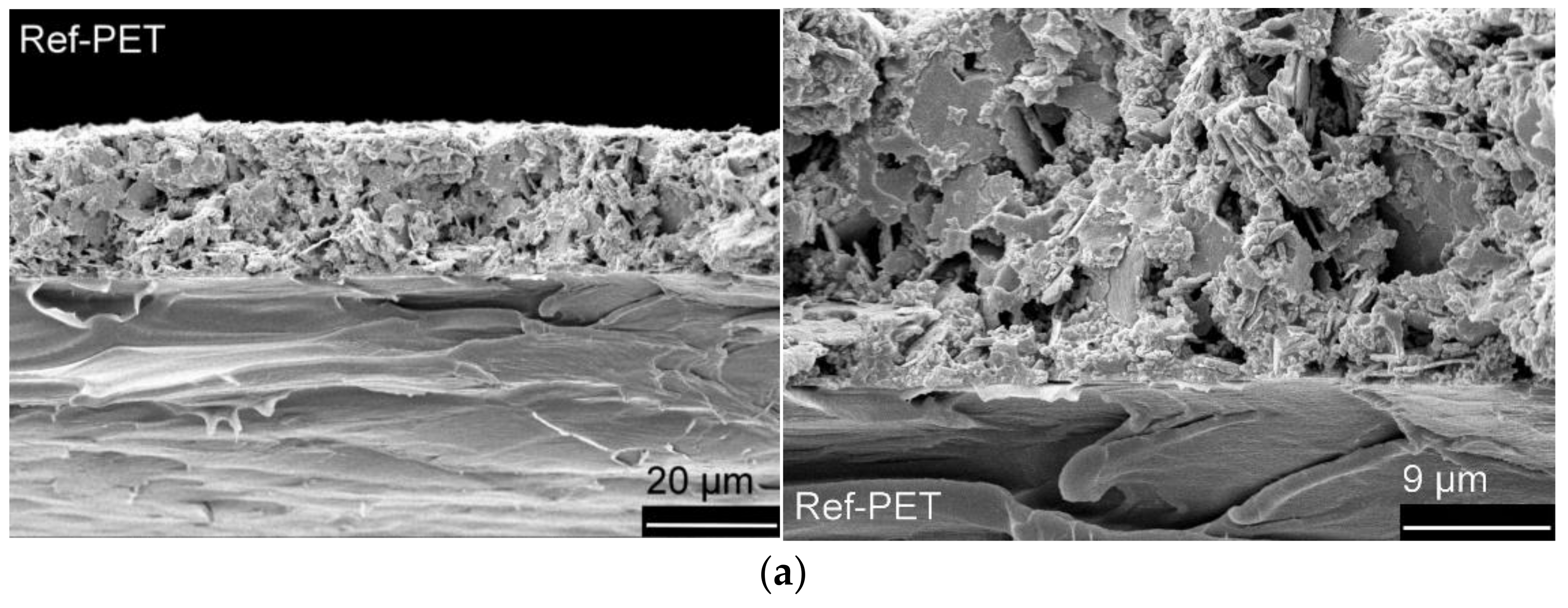
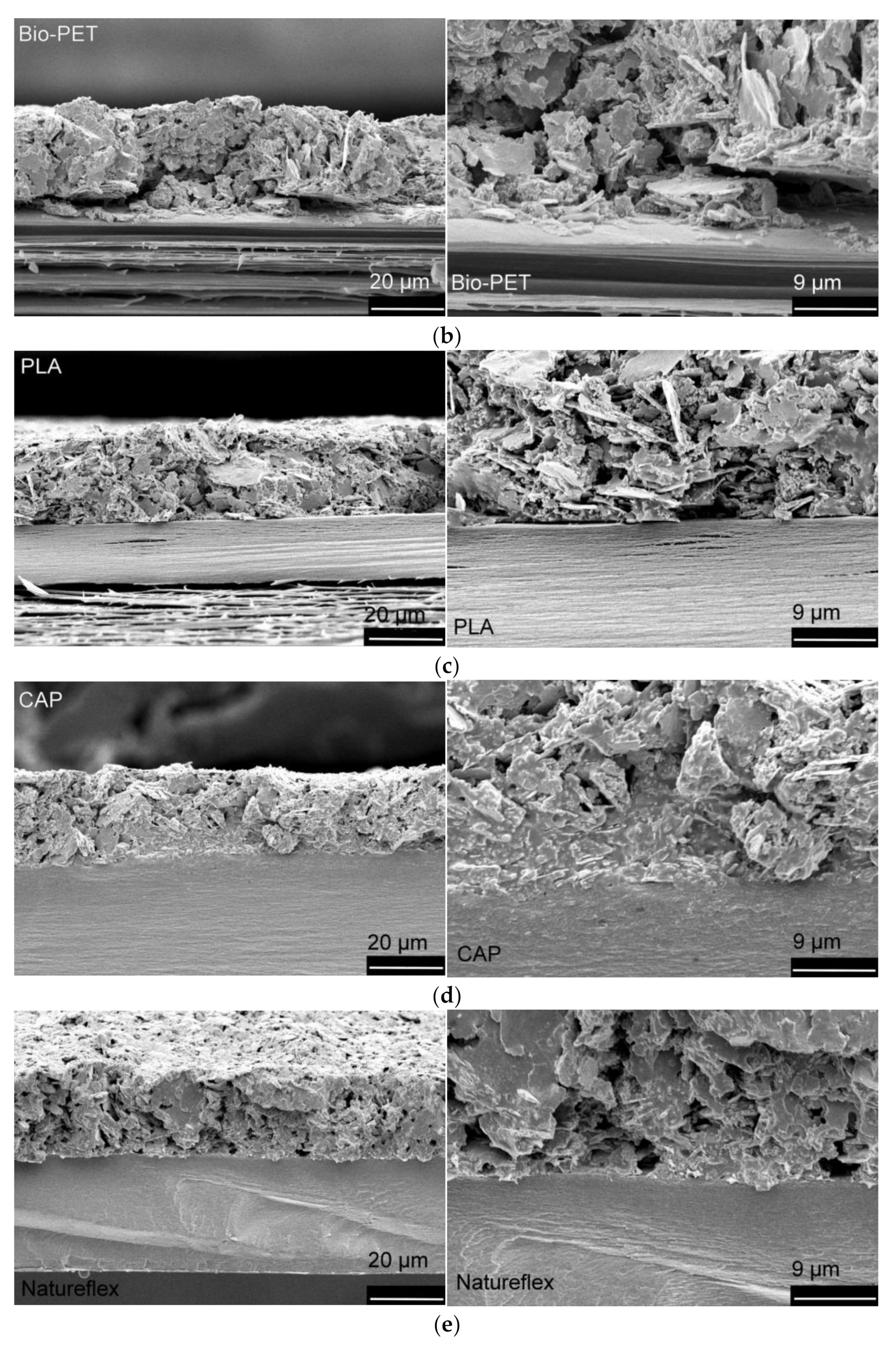
3.5. SEM Analysis for S2S Screen-Printed Films
4. Conclusions
Author Contributions
Funding
Institutional Review Board Statement
Informed Consent Statement
Data Availability Statement
Acknowledgments
Conflicts of Interest
References
- Nathan, A.; Ahnood, A.; Cole, M.T.; Lee, S.; Suzuki, Y.; Hiralal, P.; Bonaccorso, F.; Hasan, T.; Garcia-Gancedo, L.; Dyadyusha, A.; et al. Flexible electronics: The next ubiquitous platform. Proc. IEEE 2012, 100, 1486–1517, Special Centennial Issue. [Google Scholar] [CrossRef]
- Hoeng, F.; Denneulin, A.; Bras, J. Use of nanocellulose in printed electronics: A review. Nanoscale 2016, 8, 13131–13154. [Google Scholar] [CrossRef] [PubMed]
- Khan, Y.; Thielens, A.; Muin, S.; Ting, J.; Baumbauer, C.; Arias, A.C. A New Frontier of Printed Electronics: Flexible Hybrid Electronics. Adv. Mater. 2020, 32, 1905279. [Google Scholar] [CrossRef] [PubMed]
- Välimäki, M.; Apilo, P.; Po, R.; Jansson, E.; Bernardi, A.; Ylikunnari, M.; Vilkman, M.; Corso, G.; Puustinen, J.; Tuominen, J.; et al. R2R-printed inverted OPV modules-Towards arbitrary patterned designs. Nanoscale 2015, 7, 9570–9580. [Google Scholar] [CrossRef] [PubMed]
- Luoma, E.; Välimäki, M.; Rokkonen, T.; Sääskilahti, H.; Ollila, J.; Rekilä, J.; Immonen, K.E. Oriented and annealed poly(lactic acid) films and their performance in flexible printed and hybrid electronics. J. Plast. Film Sheeting 2021, 37, 429–462. [Google Scholar] [CrossRef]
- Liu, P.; He, W.; Lu, A. Preparation of low-temperature sintered high conductivity inks based on nanosilver self-assembled on surface of graphene. J. Cent. South Univ. 2019, 26, 2953–2960. [Google Scholar] [CrossRef]
- DuPont de Nemours Inc. Printed Electronic Materials-Low Temperature Electronic Inks. Available online: https://www.dupont.com/products/low-temperature-electronic-inks.html (accessed on 31 March 2022).
- Khan, S.; Lorenzelli, L.; Dahiya, R.S. Technologies for printing sensors and electronics over large flexible substrates: A review. IEEE Sens. J. 2015, 15, 3164–3185. [Google Scholar] [CrossRef]
- Keränen, K.; Korhonen, P.; Rekilä, J.; Tapaninen, O.; Happonen, T.; Makkonen, P.; Rönkä, K. Roll-to-roll printed and assembled large area LED lighting element. Int. J. Adv. Manuf. Technol. 2015, 81, 529–536. [Google Scholar] [CrossRef] [Green Version]
- UN Sustainable Development Goals. Available online: https://sdgs.un.org/goals (accessed on 19 April 2022).
- EU Bioeconomy Strategy. Available online: https://ec.europa.eu/info/research-and-innovation/research-area/environment/bioeconomy/bioeconomy-strategy_en (accessed on 19 April 2022).
- EU Plastic Strategy. Available online: https://ec.europa.eu/environment/strategy/plastics-strategy_en (accessed on 19 April 2022).
- Reddy, M.M.; Vivekanandhan, S.; Misra, M.; Bhatia, S.K.; Mohanty, A.K. Biobased plastics and bionanocomposites: Current status and future opportunities. Prog. Polym. Sci. 2013, 38, 10–11. [Google Scholar] [CrossRef]
- Andreeßen, C.; Steinbüchel, A. Recent developments in non-biodegradable biopolymers: Precursors, production processes, and future perspectives. Appl. Microbiol. Biotechnol. 2019, 103, 143–157. [Google Scholar] [CrossRef]
- Jabarin, S.A. Orientation studies of polyethylene terephthalate. Polym. Eng. Sci. 1984, 24, 376–384. [Google Scholar] [CrossRef]
- Bandla, S.; Allahkarami, M.; Hanan, J.C. Out-of-plane orientation and crystallinity of biaxially stretched polyethylene terephthalate. Powder Diffr. 2014, 29, 123–126. [Google Scholar] [CrossRef] [Green Version]
- Groeninckx, G.; Berghmans, H.; Overbergh, N.; Smets, G. Crystallization of poly(ethylene terephthalate) induced by inorganic compounds. I. Crystallization behaviour from the glassy state in a low-temperature region. J. Polym. Sci. B Polym. Phys. Polymer Phys. Ed. Abbr. 1974, 12, 303–316. [Google Scholar] [CrossRef]
- Bioplastics Market Data. Available online: https://www.european-bioplastics.org/market/ (accessed on 31 March 2022).
- Farah, S.; Anderson, D.G.; Langer, R. Physical and mechanical properties of PLA, and their functions in widespread applications—A comprehensive review. Adv. Drug Deliv. Rev. 2016, 107, 367–392. [Google Scholar] [CrossRef] [PubMed] [Green Version]
- Castro-Aguirre, E.; Iñiguez-Franco, F.; Samsudin, H.; Fang, X.; Auras, R. Poly(lactic acid)—Mass production, processing, industrial applications, and end of life. Adv. Drug Deliv. Rev. 2016, 107, 333–366. [Google Scholar] [CrossRef] [PubMed] [Green Version]
- Välimäki, M.K.; Sokka, L.I.; Peltola, H.B.; Ihme, S.S.; Rokkonen, T.M.J.; Kurkela, T.J.; Ollila, J.T.; Korhonen, A.T.; Hast, J.T. Printed and hybrid integrated electronics using bio-based and recycled materials—increasing sustainability with greener materials and technologies. Int. J. Adv. Manuf. Technol. 2020, 111, 325–339. [Google Scholar] [CrossRef]
- White, A.W.; Buschanan, C.M.; Pearcy, B.G.; Wood, M.D. Mechanical properties of cellulose acetate propionate/aliphatic polyester blends. J. Appl. Polym. Sci. 1994, 52, 525–530. [Google Scholar] [CrossRef]
- Albis Plastics Data for Cellidor®. Available online: www.albis.com (accessed on 31 March 2022).
- Abd Manaf, M.E.; Nitta, K.H.; Yamaguchi, M. Mechanical properties of plasticized cellulose ester films at room and high temperatures. ARPN J. Eng. Appl. Sci. 2006, 11, 2354–2358. [Google Scholar]
- Eastman EastmanTM Cellulose-Based Specialty Polymers. Available online: https://cms.chempoint.com/ChemPoint/media/ChemPointSiteMedia/General-CE-Brochure.pdf (accessed on 31 March 2022).
- Edgar, K.J.; Buchanan, C.M.; Debenham, J.S.; Rundquist, P.A.; Seiler, B.D.; Shelton, M.C.; Tindall, D. Advances in cellulose ester performance and application. Prog. Polym. Sci. 2001, 26, 1605–1688. [Google Scholar] [CrossRef]
- Hyden, W.L. Manufacture and Properties of Regenerated Cellulose Films. Ind. Eng. Chem. 1929, 21, 405–410. [Google Scholar] [CrossRef]
- APG Global Data for Cellophane. Available online: http://www.apgglobe.com/en/cellophane/ (accessed on 31 March 2022).
- Bajpai, P. Biermann’s Handbook of Pulp and Paper, 3rd ed.; Elsevier Ltd.: Amsterdam, The Netherlands, 2018; pp. 233–247. [Google Scholar]
- El Seoud, O.A.; Kostag, M.; Jedvert, K.; Malek, N.I. Cellulose Regeneration and Chemical Recycling: Closing the ‘Cellulose Gap’ Using Environmentally Benign Solvents. Macromol. Mater. Eng. 2020, 305, 1900832. [Google Scholar] [CrossRef]
- Ge, X. Regenerated Cellulose Films from Binary Solvent Systems. Master’s Thesis, Aalto University, Espoo, Finland, July 2018. Available online: https://aaltodoc.aalto.fi/handle/123456789/33678 (accessed on 31 March 2022).
- Zhang, L.; Zhou, J.; Huang, J.; Gong, P.; Zhou, Q.; Zheng, L.; Du, Y. Biodegradability of regenerated cellulose films coated with polyurethane/natural polymers interpenetrating polymer networks. Ind. Eng. Chem. Res. 1999, 38, 4284–4289. [Google Scholar] [CrossRef]
- Zhang, Y.; Ji, Q.; Qi, H.; Liu, Z. Structure and Properties of Regenerated Cellulose Film with Fluorocarbon Coating. Phys. Procedia 2012, 32, 706–713. [Google Scholar] [CrossRef] [Green Version]
- Futamura Group Futamura NatureFlex™ Info. Available online: http://www.futamuragroup.com/en/divisions/cellulose-films/products/natureflex/heat-resistant/ (accessed on 31 March 2022).
- Brunetti, F.; Operamolla, A.; Castro-Hermosa, S.; Lucarelli, G.; Manca, V.; Farinola, G.M.; Brown, T.M. Printed Solar Cells and Energy Storage Devices on Paper Substrates. Adv. Funct. Mater. 2019, 29, 1806798. [Google Scholar] [CrossRef] [Green Version]
- Biomasspackaging. Available online: http://www.biomasspackaging.com/brands/natureflex/ (accessed on 19 April 2022).
- Rapisarda, M.; Patanè, C.; Pellegrino, A.; Malvuccio, A.; Rizzo, V.; Muratore, M.; Rizzarelli, P. Compostable Polylactide and Cellulose Based Packaging for Fresh-Cut Cherry Tomatoes: Performance Evaluation and Influence of Sterilization Treatment. Materials 2020, 13, 3432. [Google Scholar] [CrossRef] [PubMed]
- DuPontTeijinFilms MELINEX® ST506 Datasheet. Available online: https://usa.dupontteijinfilms.com/wp-content/uploads/2017/01/ST506-Datasheet.pdf (accessed on 31 March 2022).
- Jabarin, S.A. Strain-induced crystallization of poly(ethylene terephthalate). Polym. Eng. Sci. 1992, 32, 1341–1349. [Google Scholar] [CrossRef]
- Sichina, W.J. DSC as Problem Solving Tool: Measurement of Percent Crystallinity of Thermoplastics, Application Note. Available online: https://www.perkinelmer.com/Content/applicationnotes/app_thermalcrystallinitythermoplastics.pdf (accessed on 31 March 2022).
- Wu, J.H.; Yen, M.S.; Wu, C.P.; Li, C.H.; Kuo, M.C. Effect of Biaxial Stretching on Thermal Properties, Shrinkage and Mechanical Properties of Poly (Lactic Acid) Films. J. Polym. Environ. 2013, 21, 303–311. [Google Scholar] [CrossRef]
- Aydemir, C.; Altay, B.N.; Akyol, M. Surface analysis of polymer films for wettability and ink adhesion. Color Res. Appl. 2021, 46, 489–499. [Google Scholar] [CrossRef]
- Petasch, W.; Räuchle, E.; Walker, M.; Elsner, P. Improvement of the adhesion of low-energy polymers by a short-time plasma treatment. Surf. Coatings Technol. 1995, 74–75, 682–688. [Google Scholar] [CrossRef]

| Material | Screw | RPM | Temperature Profile from Die to Feeder | Chill Roll Temperature (°C) | Film Thickness (μm) |
|---|---|---|---|---|---|
| Bio-PET | 3:1 | 50 | 270–270–270–270–270–270 °C | 80 | 700 |
| PLA | 3:1 | 50 | 205–205–200–200–200–200 °C | 60 | 650–700 |
| CAP | 3:1 | 50 | 210–210–210–200–200–200 °C | 80 | 650–700 |
| Material | Temperature (°C) | Pre-Heating Time (s) | BO Ratio | Stretch Rate (%/s) | Thickness after (μm) |
|---|---|---|---|---|---|
| Bio-PET | 88 | 120 | 2.9 × 2.9 | 100 | 80–100 |
| PLA | 77 | 120 | 2.9 × 2.9 | 100 | 80–100 |
| CAP | 137 | 90 | 2.1 × 2.1 | 100 | 150–170 |
| Material | |
|---|---|
| PET [40] | 140.1 |
| PLA [41] | 93.6 |
| Material | Tg (°C) | Tcc (°C) | Tm (°C) | Tmc (°C) |
|---|---|---|---|---|
| Ref-PET | 77.7 ± 0.0 | 254.1 ± 1.5 | 195.9 ± 1.2 | |
| Bio-PET | 72.3 ± 0.0 | 131.3 ± 0.20 | 248.8 ± 0.7 | 186.3 ± 0.4 |
| Bio-PET BO | 83.5 ± 0.0 | − | 249.3 ± 0.1 | 188.8 ± 0.6 |
| Bio-PET BO annealed | 80.5 ± 0.2 | − | 248.7 ± 0.1 | 186.8 ± 0.1 |
| PLA | 60.3 ± 0.1 | 107.9 ± 0.1 | 176.9 ± 0.3 | − |
| PLA BO | 66.9 ± 0.1 | 93.5 ± 3.3 | 176.5 ± 0.0 | − |
| PLA BO annealed | 65.7 ± 0.1 | − | 175.6 ± 0.3 | − |
| CAP | 97.0 ± 1.1 | − | 155.8 ± 0.1 | − |
| CAP BO | 102.1 ± 0.2 | − | 158.4 ± 1.2 | − |
| CAP BO annealed | 109.5 ± 3.5 | − | 162.7 ± 1.4 | − |
| Natureflex | 68.2 ± 0.0 | − | 178.9 ± 0.0 | − |
| Sample | ΔHm (J/g) | ΔHcc (J/g) | XC (%) |
|---|---|---|---|
| Ref-PET | 62.7 ± 3.7 | − | 44.7 ± 2.6 |
| Bio-PET | 40.6 ± 1.2 | 31.4 ± 0.6 | 6.5 ± 0.4 |
| Bio-PET BO | 50.7 ± 0.2 | − | 36.2 ± 0.1 |
| Bio-PET BO annealed | 46.7 ± 0.6 | − | 33.3 ± 0.4 |
| PLA | 45.7 ± 1.4 | 46.3 ± 0.10 | 0.0 ± 1.33 |
| PLA BO | 61.0 ± 2.4 | 31.6 ± 1.2 | 31.4 ± 3.9 |
| PLA BO annealed | 48.8 ± 1.0 | 2.9 ± 1.2 | 49.0 ± 2.3 |
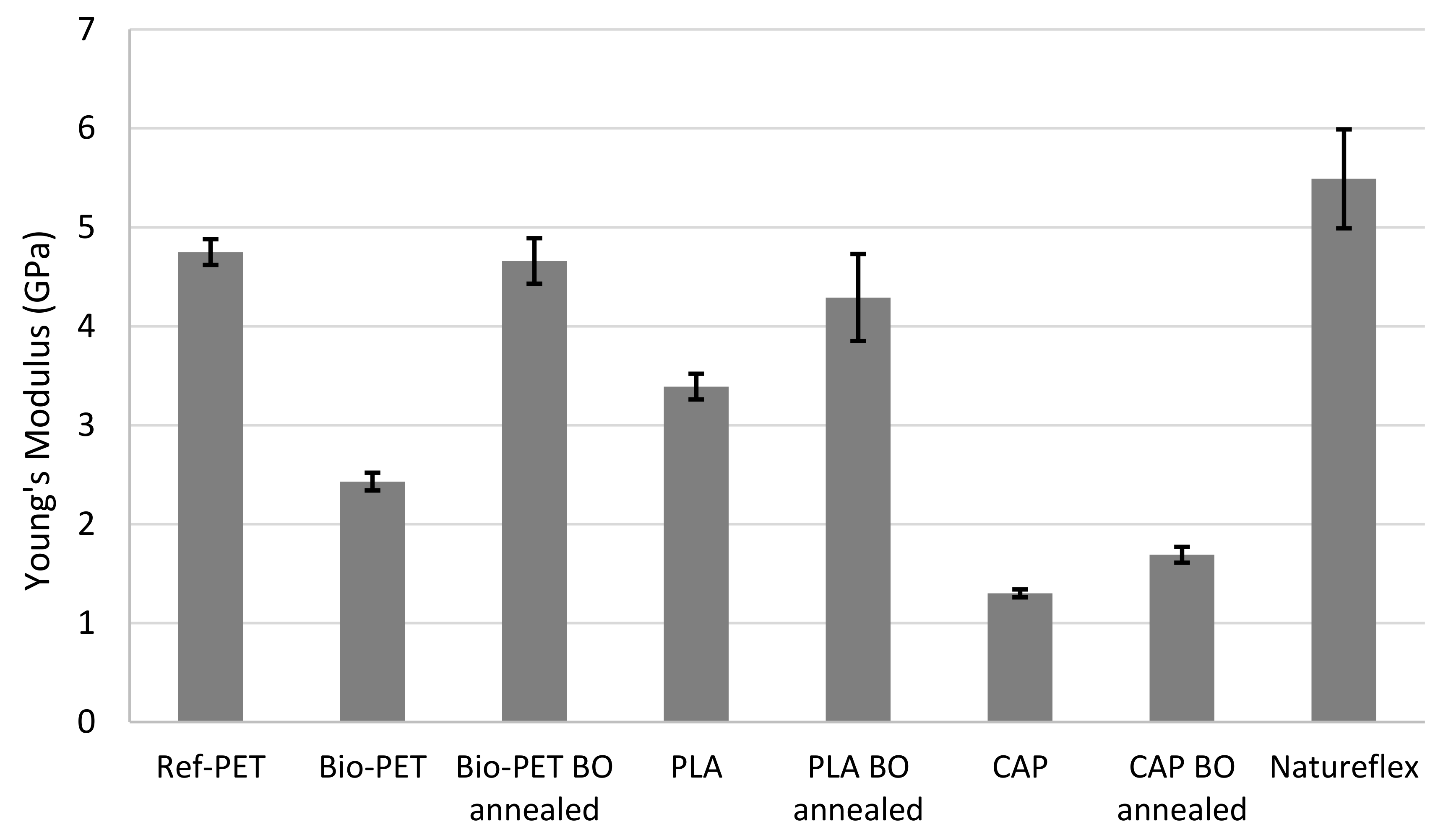
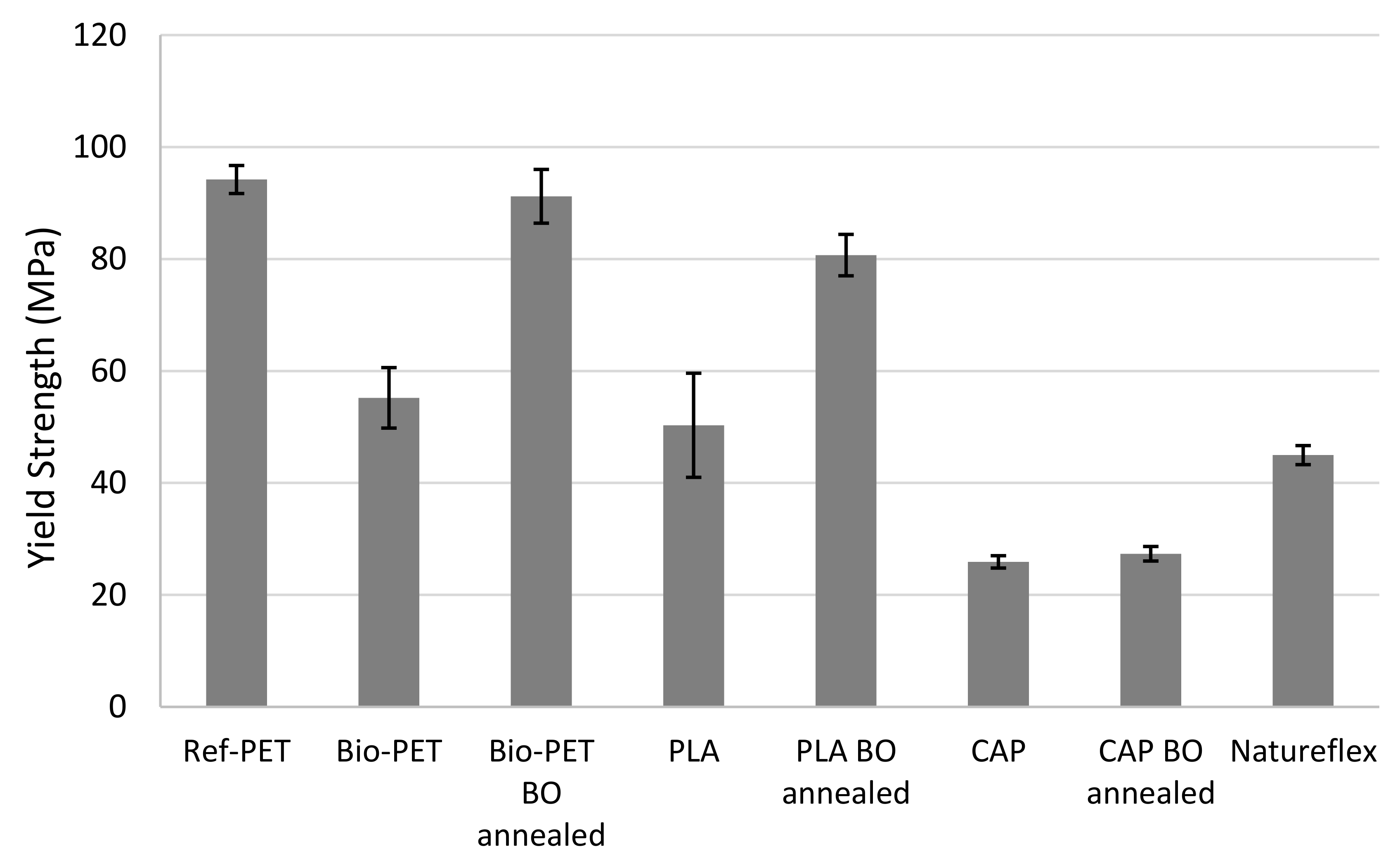
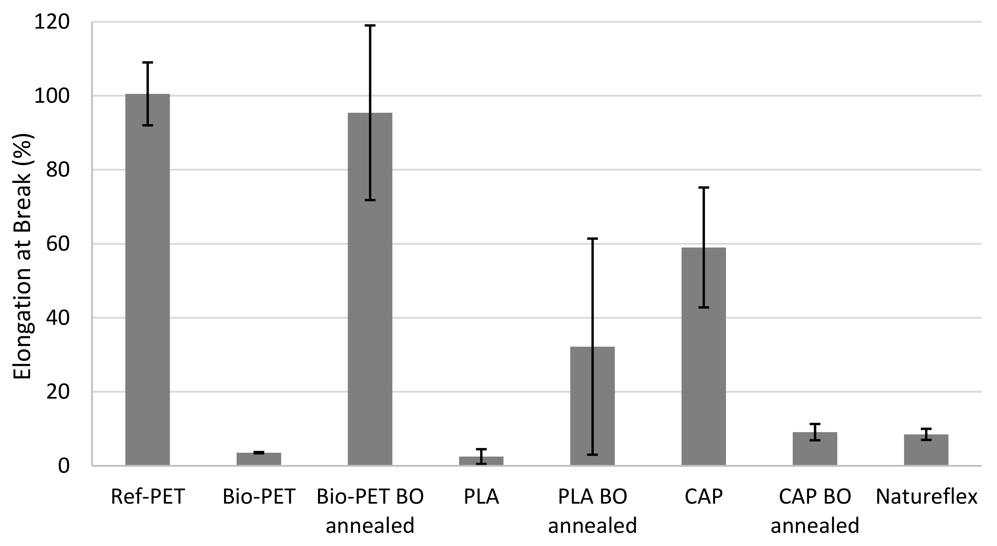
| Sample | Young’s Modulus (GPa) | Yield Strength (MPa) | Strain at Break (%) |
|---|---|---|---|
| Ref-PET | 4.75 ± 0.13 | 94.2 ± 2.5 | 100.5 ± 8.5 |
| Bio-PET | 2.43 ± 0.09 | 55.2 ± 5.4 | 3.55 ± 0.17 |
| Bio-PET BO annealed | 4.66 ± 0.23 | 91.2 ± 4.8 | 95.4 ± 23.6 |
| PLA | 3.39 ± 0.13 | 50.3 ± 9.3 | 2.5 ± 2.0 |
| PLA BO annealed | 4.29 ± 0.44 | 80.7 ± 3.7 | 32.2 ± 29.2 |
| CAP | 1.30 ± 0.04 | 25.9 ± 1.1 | 59.0 ± 16.2 |
| CAP BO annealed | 1.69 ± 0.08 | 27.35 ± 1.3 | 9.1 ± 2.2 |
| Natureflex | 5.49 ± 0.50 | 44.97 ± 1.7 | 8.5 ± 1.5 |
| Substrate | Ra (nm) | Rq (nm) | Rt (µm) | T (%) @500 nm | T (%) @700 nm |
|---|---|---|---|---|---|
| Ref-PET | 7 ± 2 | 9 ± 2 | 0.3 ± 0.1 | 89 | 90 |
| Bio-PET BO Annealed | 4 ± 0 | 6 ± 1 | 0.4 ± 0.1 | 88 | 89 |
| PLA BO Annealed | 9 ± 1 | 37 ± 7 | 2.2 ± 0.5 | 93 | 94 |
| CAP BO Annealed | 23 ± 7 | 36 ± 5 | 1.6 ± 0.1 | 81 | 89 |
| Natureflex | 105 ± 12 | 184 ± 20 | 3.7 ± 0.1 | 90 | 91 |
| Substrate | SFE Dispersive Part (mN/m) | SFE Polar Part (mN/m) | SFE Total (mN/m) |
|---|---|---|---|
| Ref-PET | 34.42 | 9.60 | 44.02 |
| Bio-PET BO Annealed | 38.64 | 1.76 | 40.39 |
| PLA BO Annealed | 31.34 | 6.78 | 38.12 |
| CAP BO Annealed | 32.06 | 7.90 | 39.96 |
| Natureflex | 36.40 | 0.80 | 37.20 |
| Substrate | Process T (°C) | Mean Dev MD (%) | Max; Min Dev MD (%) | Mean Dev TD (%) | Max; Min Dev TD (%) |
|---|---|---|---|---|---|
| Ref-PET | 120 | 0.00 | 0.02; −0.01 | 0.12 | 0.17; 0.07 |
| Bio-PET BO Annealed | 100 | −0.77 | −0.49; −1.18 | −0.71 | −0.48; −1.10 |
| PLA BO Annealed | 80 | −0.74 | 0.07; −1.12 | −0.52 | −0.34; −0.72 |
| CAP BO Annealed | 80 | −0.65 | −0.50; −0.79 | −0.64 | −0.10; −1.06 |
| Natureflex | 80 | −0.63 | −0.41; −0.70 | −0.54 | −0.31; −0.74 |
| Substrate | Ag Thickness (µm) | Process T (°C) | Pattern-A Mean R (Ω) | Pattern-B Mean R (Ω) | Pattern-C Mean R (Ω) |
|---|---|---|---|---|---|
| Ref-PET | 20 ± 2 | 120 | 7.2 ± 0.2 | 7.0 ± 0.2 | 12.4 ± 0.3 |
| Bio-PET BO Annealed | 21 ± 1 | 100 | 8.4 ± 0.2 | 8.3 ± 0.2 | 14.8 ± 0.6 |
| PLA BO Annealed | 23 ± 3 | 80 | 8.4 ± 0.6 | 8.1 ± 0.6 | 15.2 ± 1.3 |
| CAP BO Annealed | 18 ± 2 | 80 | 5.9 ± 0.3 | 5.7 ± 0.2 | 10.6 ± 0.4 |
| Natureflex | 21 ± 1 | 80 | 6.4 ± 0.1 | 6.3 ± 0.1 | 11.5 ± 0.3 |
Publisher’s Note: MDPI stays neutral with regard to jurisdictional claims in published maps and institutional affiliations. |
© 2022 by the authors. Licensee MDPI, Basel, Switzerland. This article is an open access article distributed under the terms and conditions of the Creative Commons Attribution (CC BY) license (https://creativecommons.org/licenses/by/4.0/).
Share and Cite
Luoma, E.; Välimäki, M.; Ollila, J.; Heikkinen, K.; Immonen, K. Bio-Based Polymeric Substrates for Printed Hybrid Electronics. Polymers 2022, 14, 1863. https://doi.org/10.3390/polym14091863
Luoma E, Välimäki M, Ollila J, Heikkinen K, Immonen K. Bio-Based Polymeric Substrates for Printed Hybrid Electronics. Polymers. 2022; 14(9):1863. https://doi.org/10.3390/polym14091863
Chicago/Turabian StyleLuoma, Enni, Marja Välimäki, Jyrki Ollila, Kyösti Heikkinen, and Kirsi Immonen. 2022. "Bio-Based Polymeric Substrates for Printed Hybrid Electronics" Polymers 14, no. 9: 1863. https://doi.org/10.3390/polym14091863
APA StyleLuoma, E., Välimäki, M., Ollila, J., Heikkinen, K., & Immonen, K. (2022). Bio-Based Polymeric Substrates for Printed Hybrid Electronics. Polymers, 14(9), 1863. https://doi.org/10.3390/polym14091863