
Effect of Stability of Two-Dimensional (2D) Aminoethyl Methacrylate Perovskite Using Lead-Based Materials for Ammonia Gas Sensor Application

 ,
,  and
and
Abstract
:
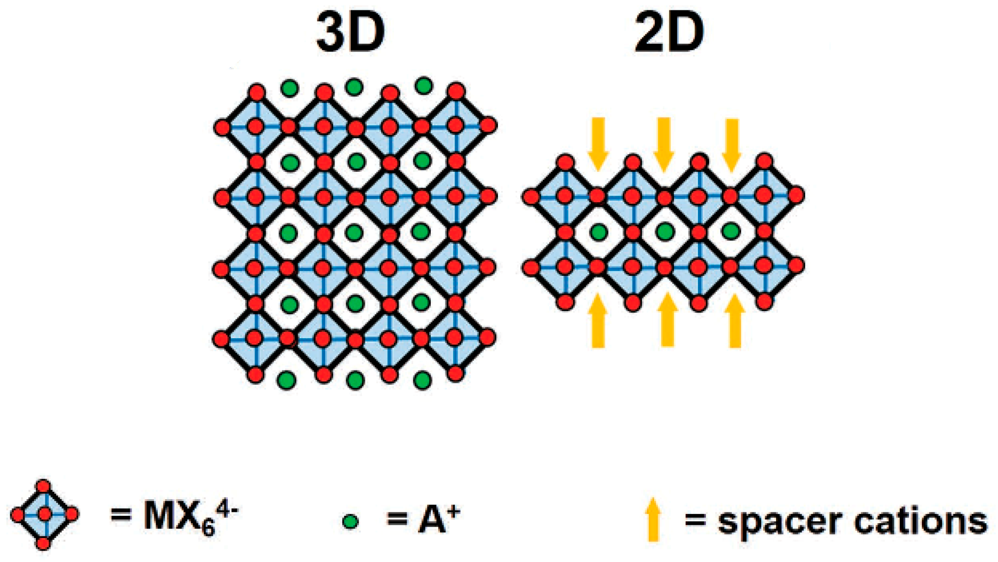
1. Introduction
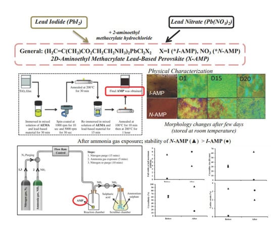
2. Materials and Methods
2.1. Materials
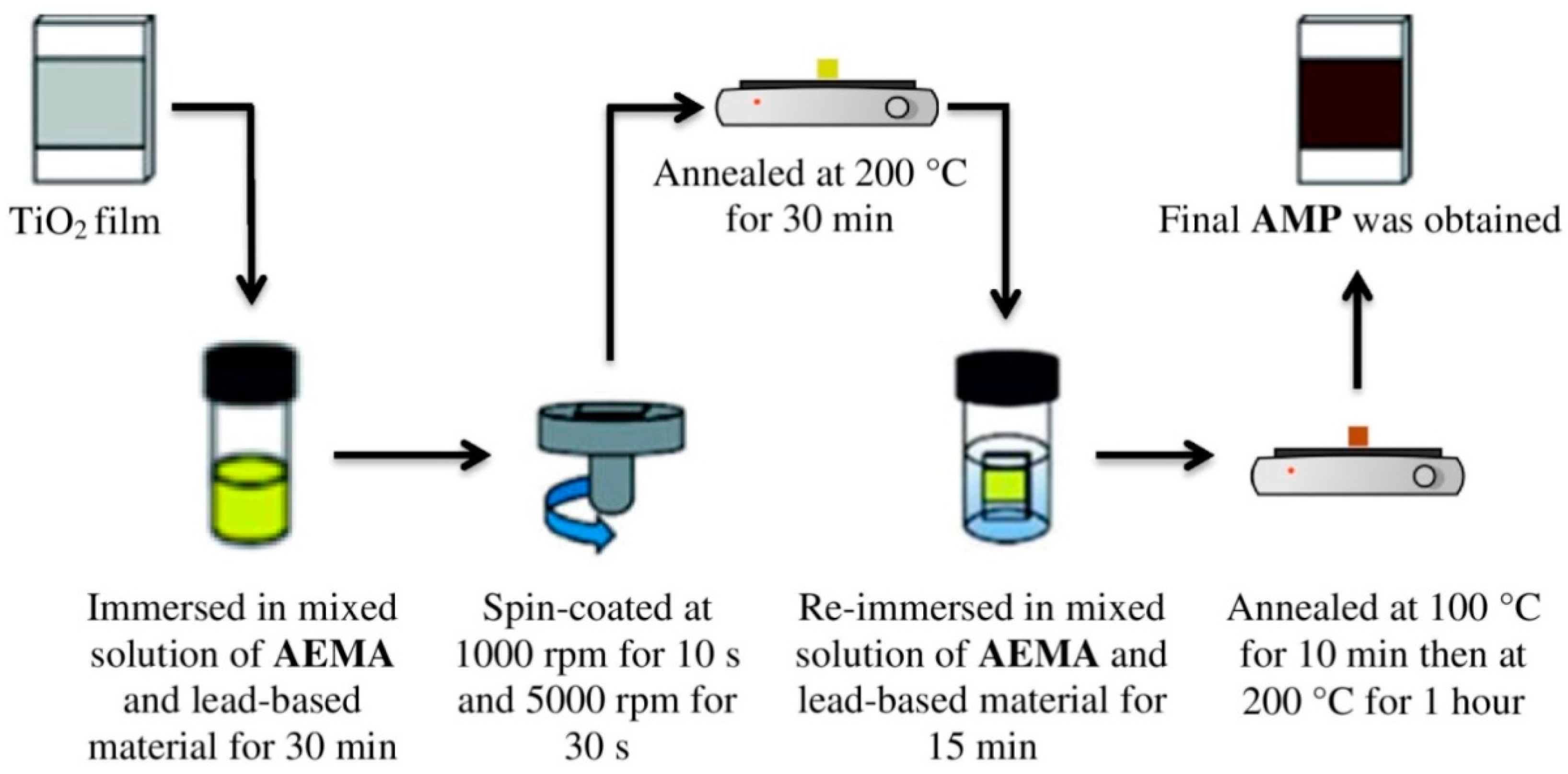
2.2. Fabrication
2.3. Characterization
3. Results and Discussion
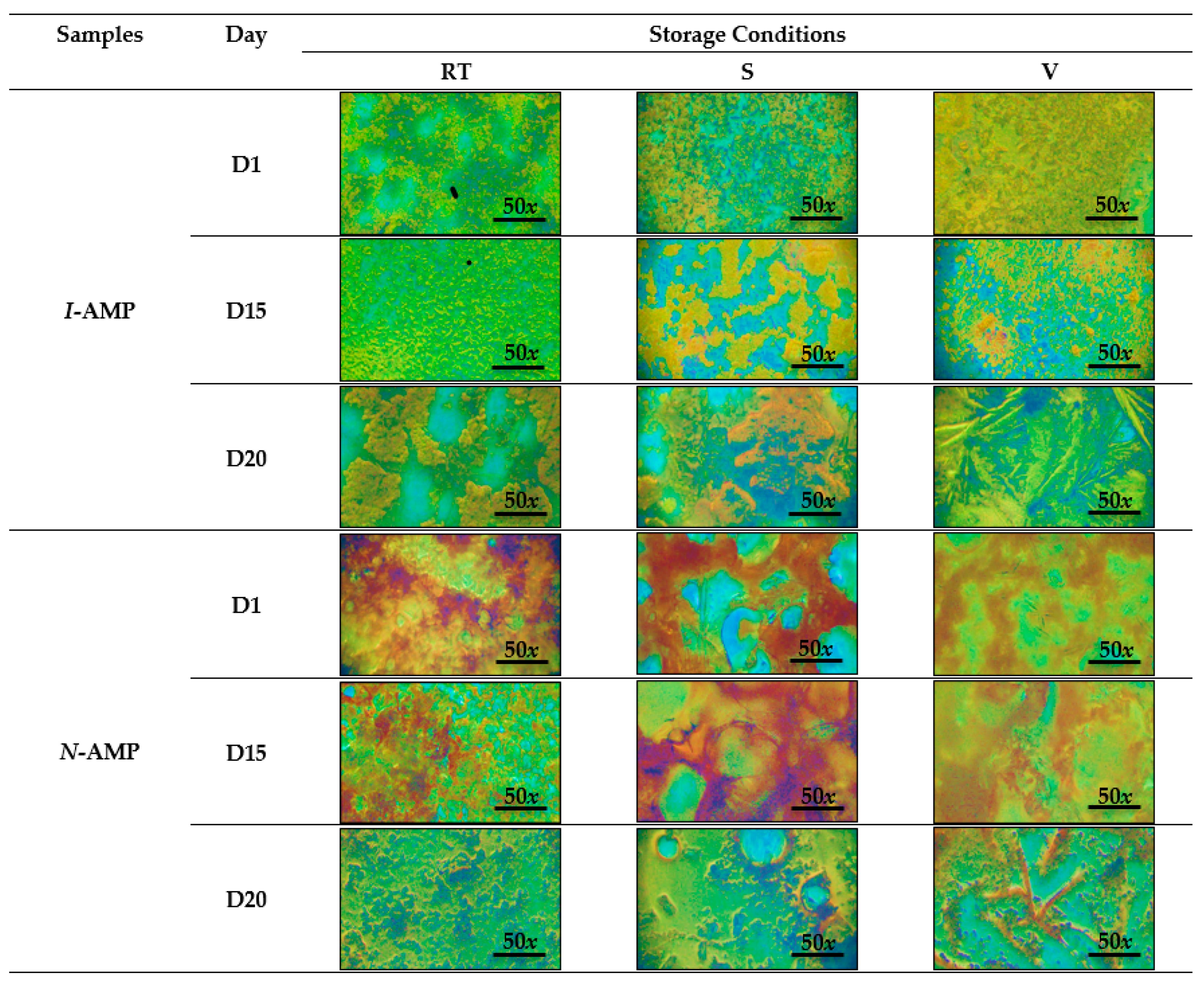
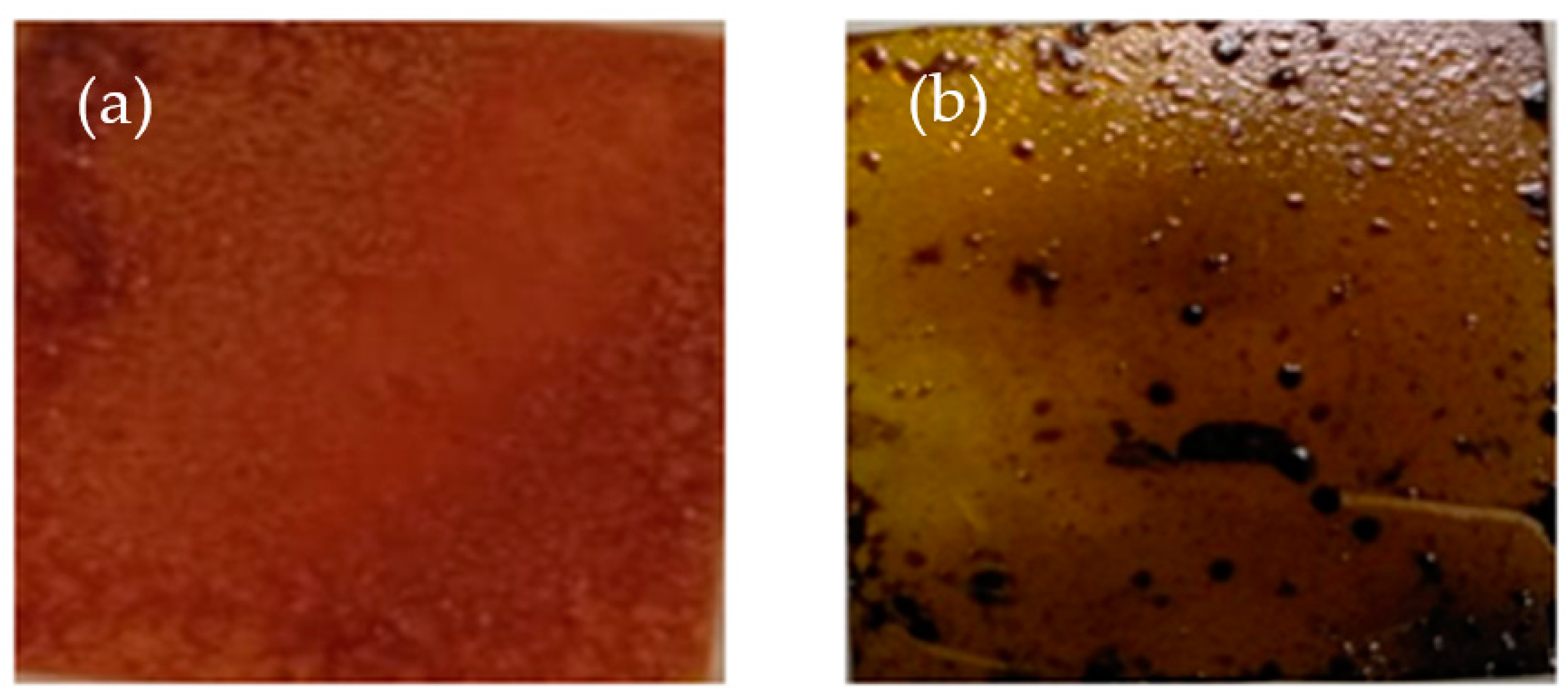
3.1. Surface Morphology
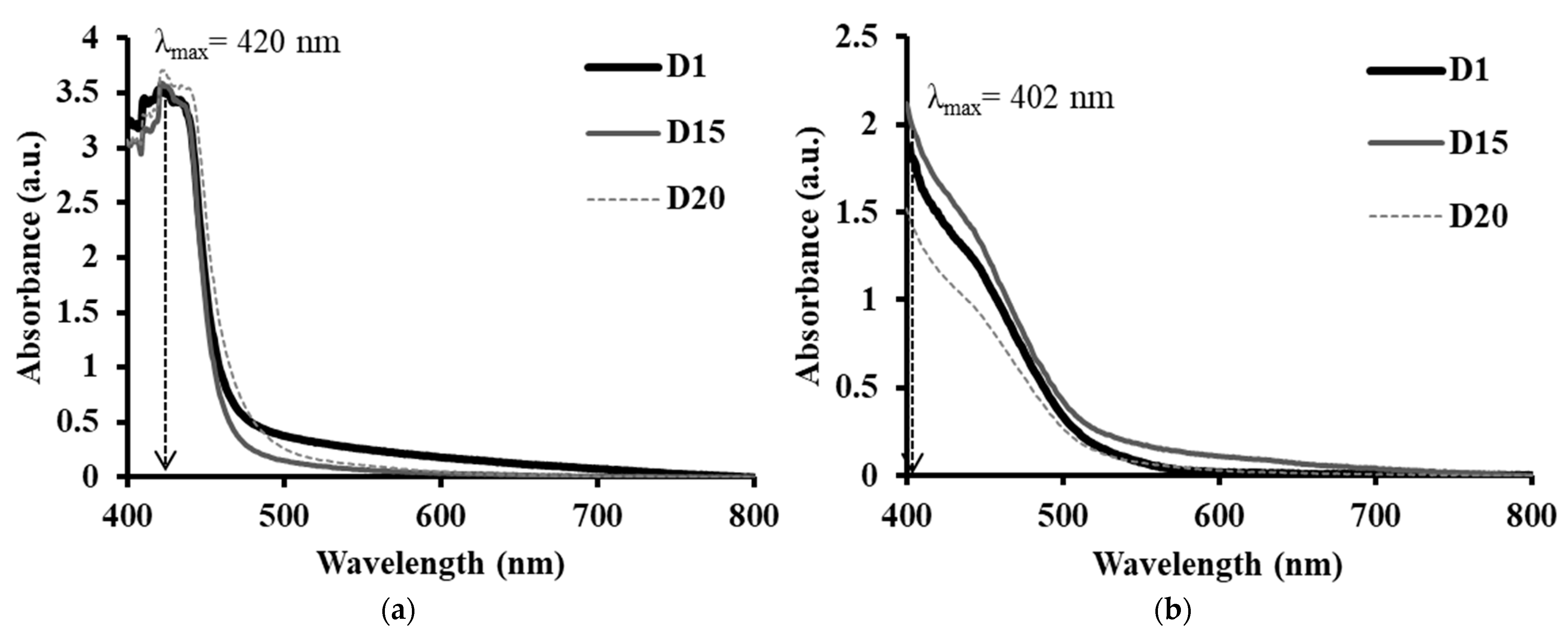
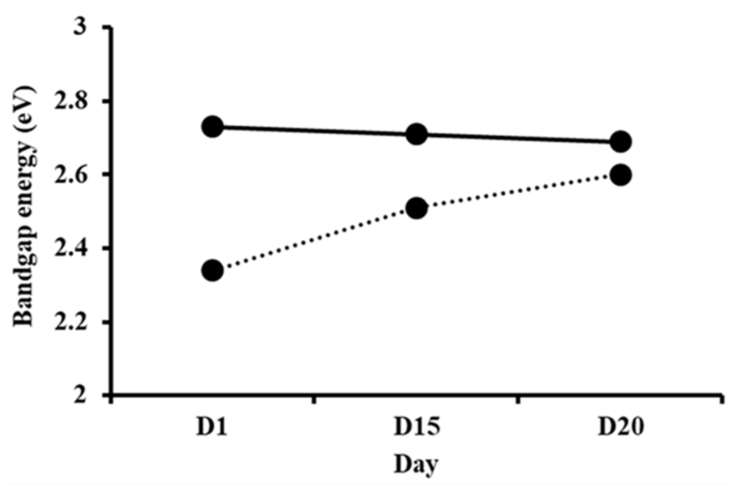
3.2. Optical Properties
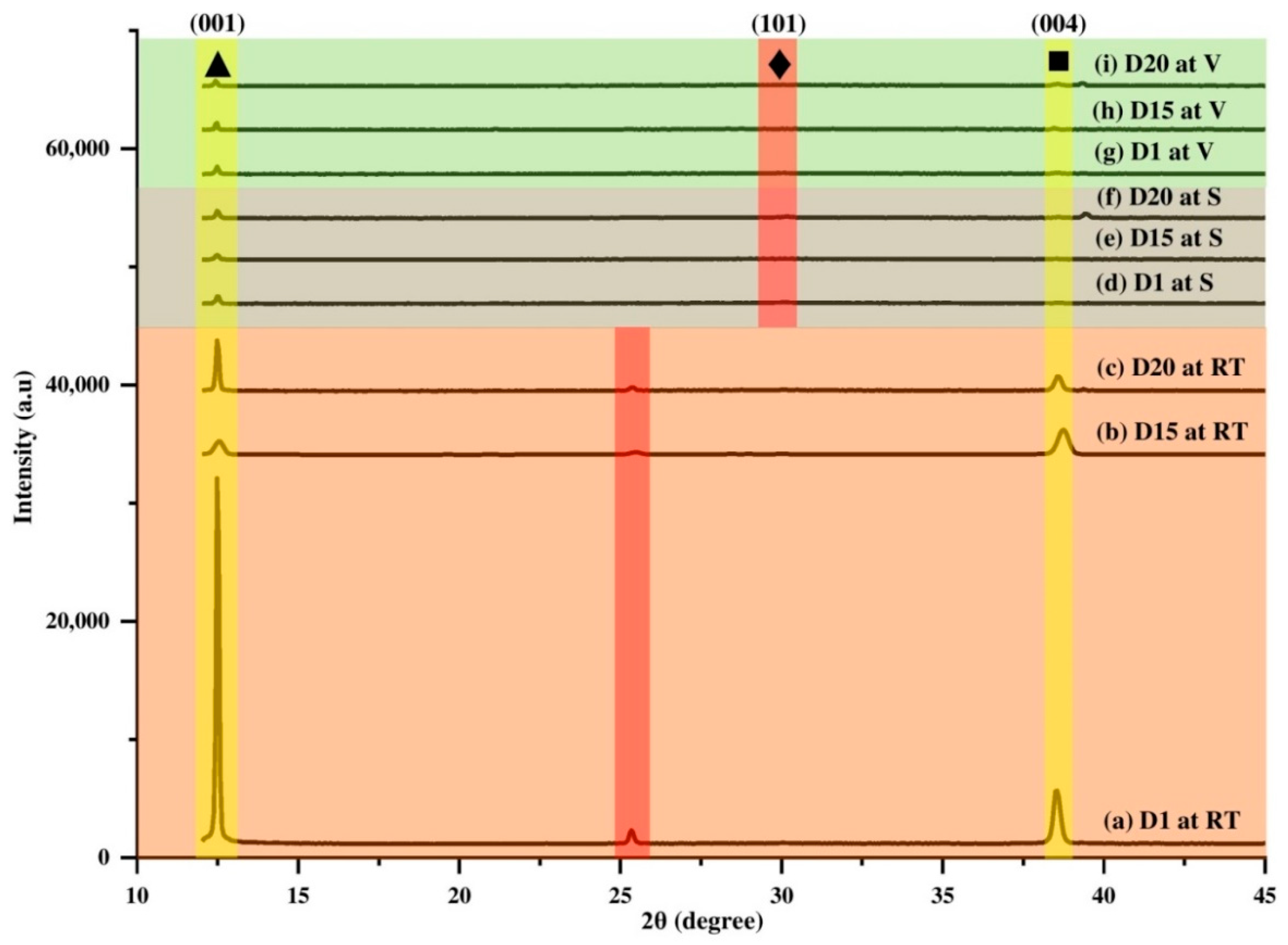
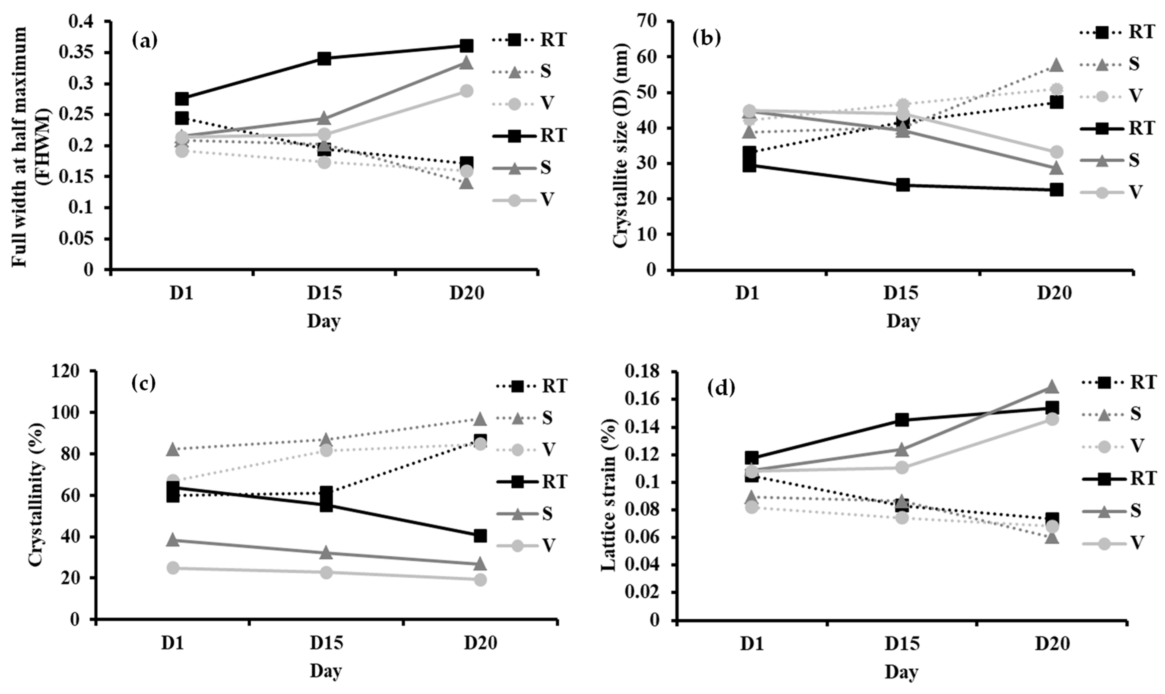
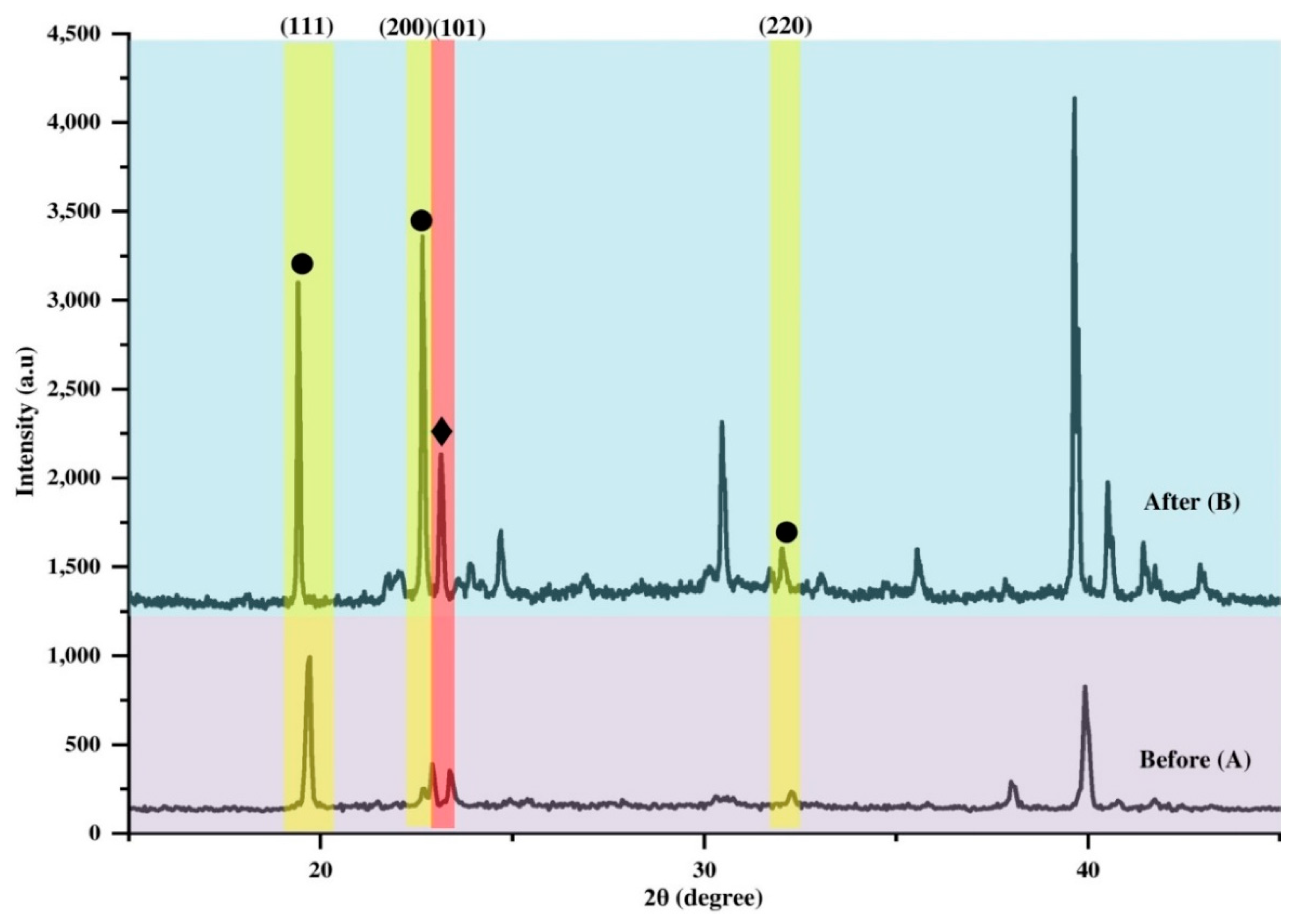
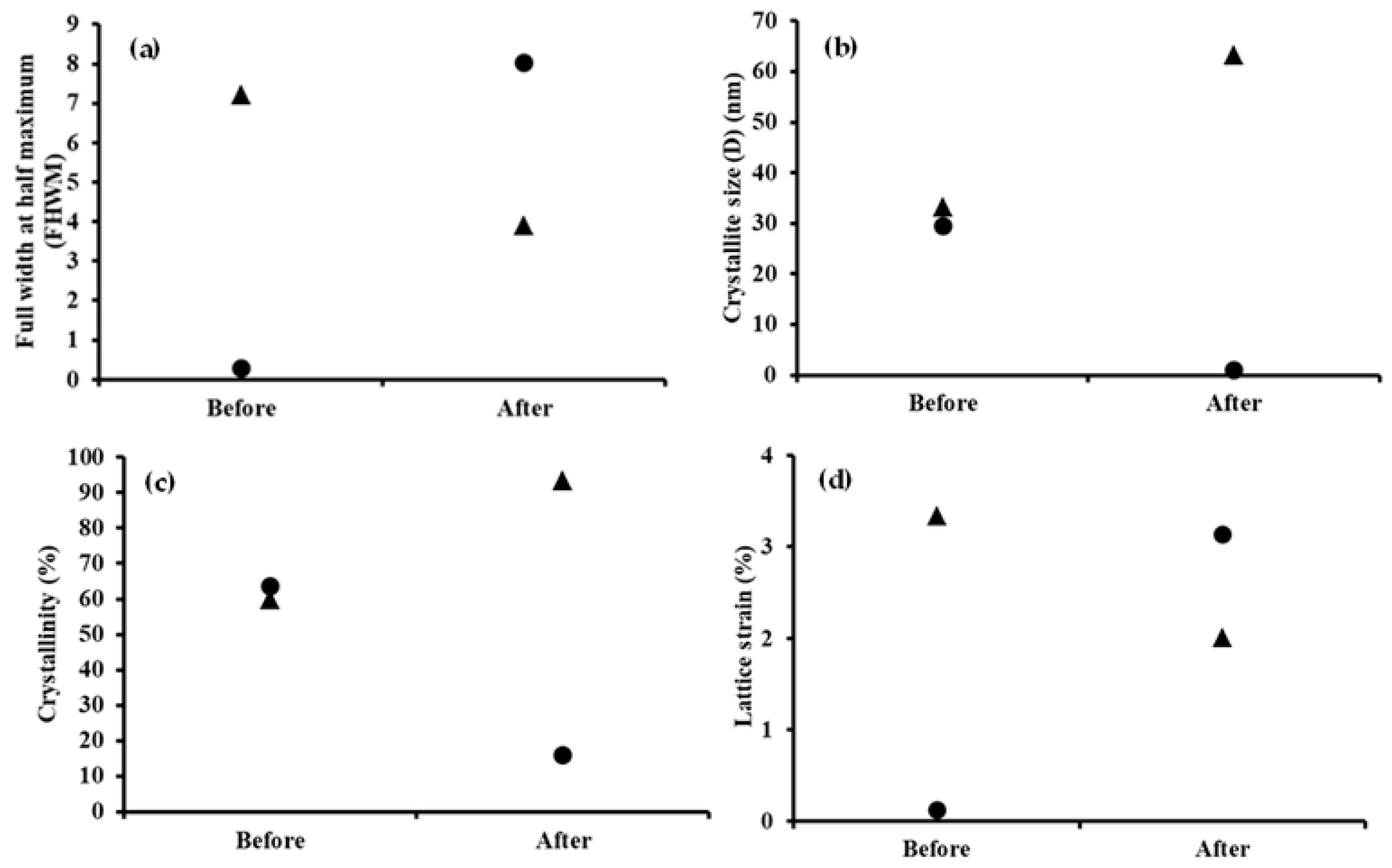
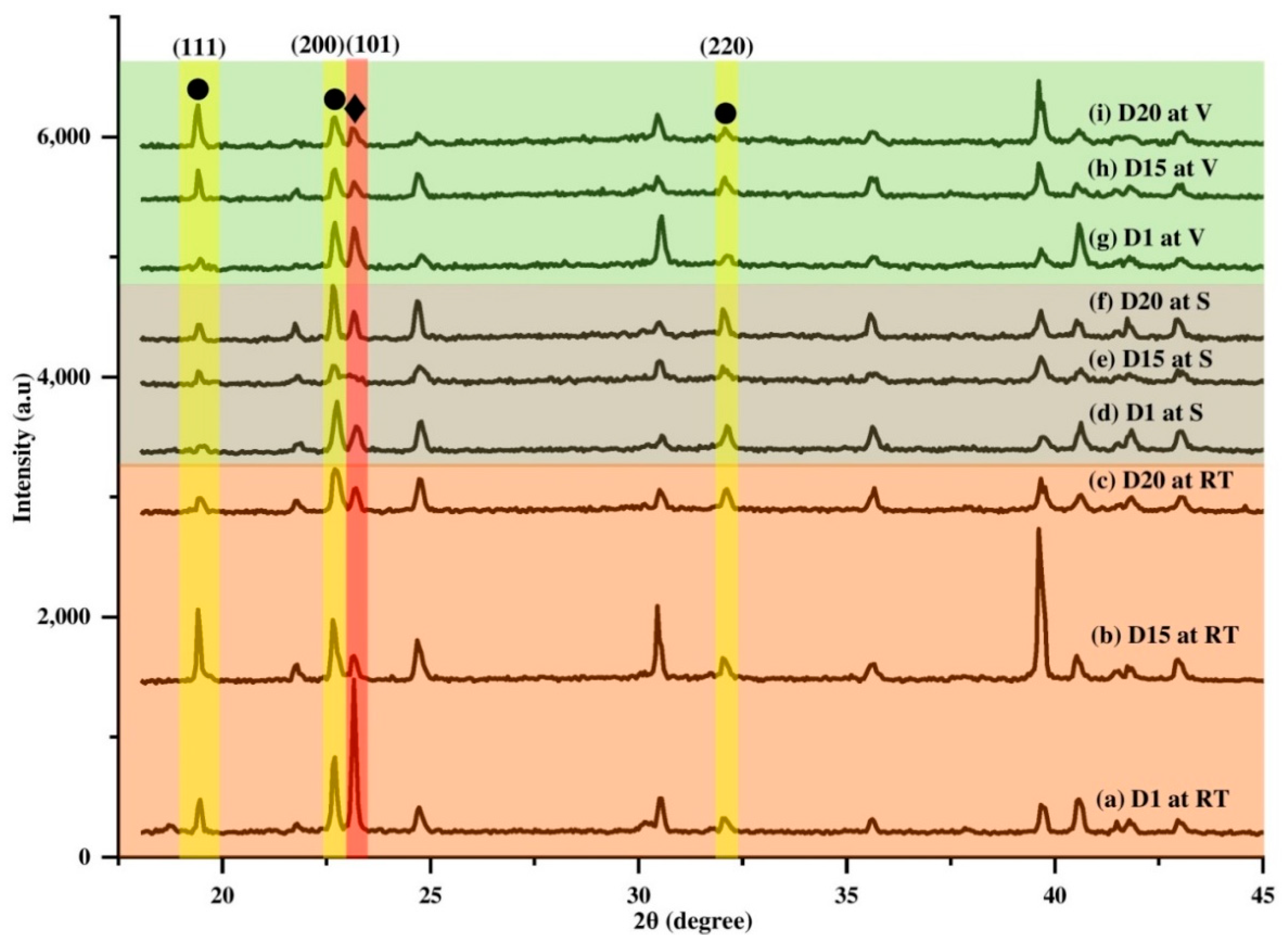
3.3. Structural and Crystallinity
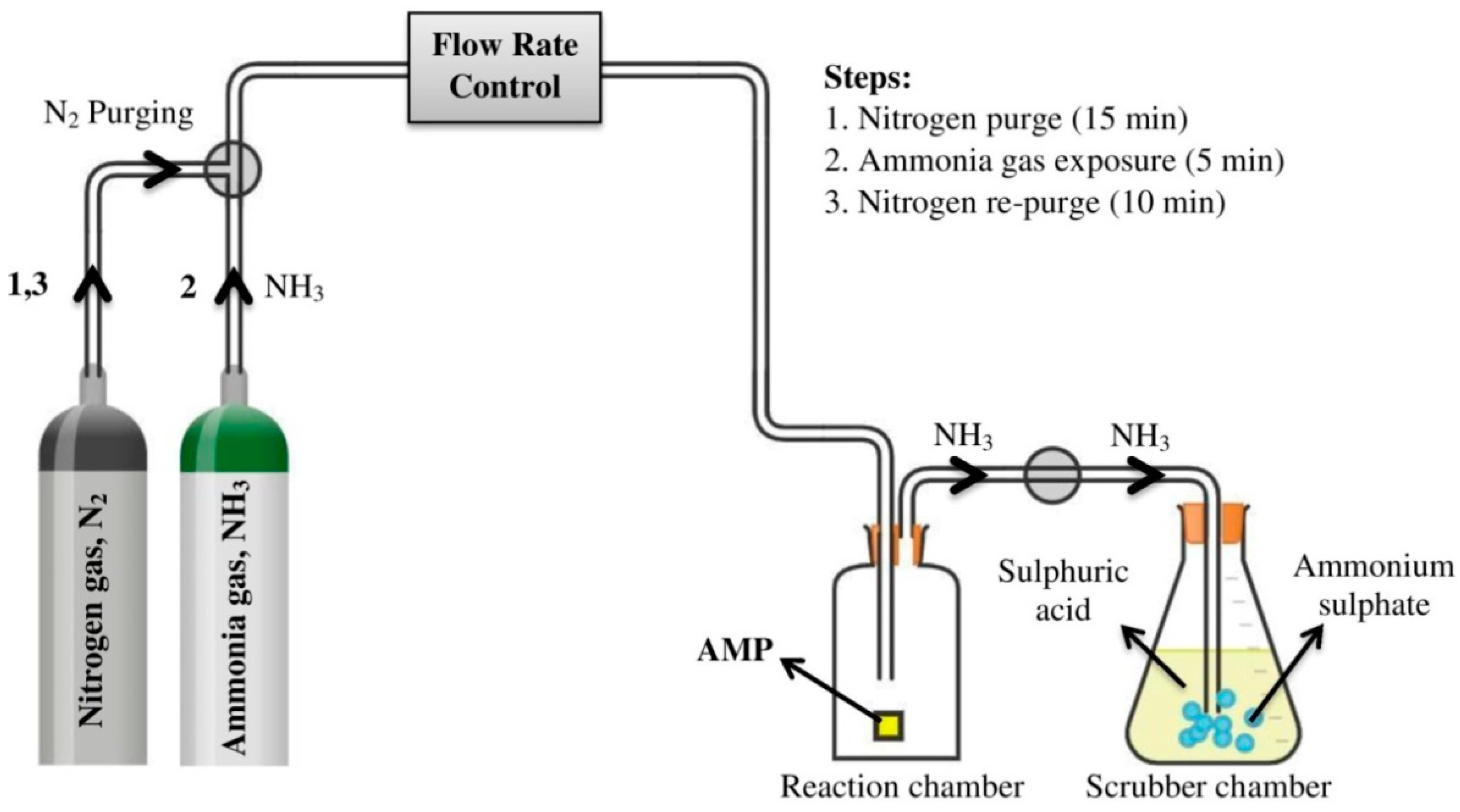
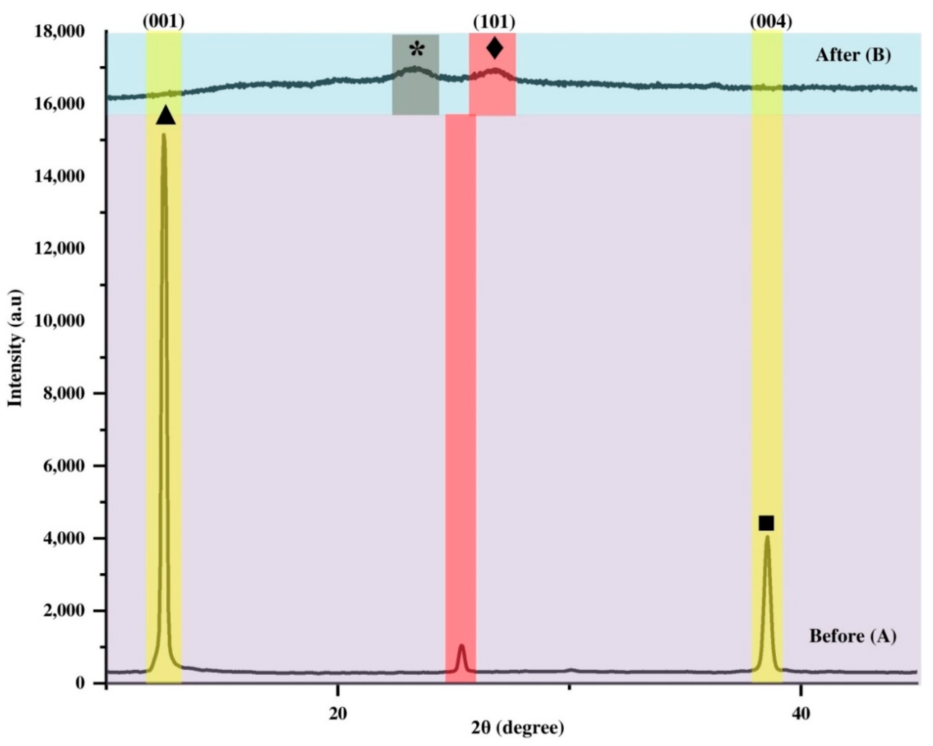
3.4. Effect of Ammonia Exposure on the Structure and Crystallinity
4. Conclusions
Supplementary Materials
Author Contributions
Funding
Institutional Review Board Statement
Informed Consent Statement
Data Availability Statement
Acknowledgments
Conflicts of Interest
References
- Varma, P.R. Low-dimensional perovskites. Perovskite Photovolt. 2018, 13, 197–229. [Google Scholar]
- Zhu, Y.; Liu, Y.; Miller, K.A.; Zhu, H.; Egap, E. Lead halide perovskite nanocrystals as photocatalysts for PET-RAFT polymerization under visible and near-infrared irradiation. ACS Macro. Lett. 2020, 9, 725–730. [Google Scholar] [CrossRef]
- Zhu, X.; Lin, Y.; Sun, Y.; Beard, M.C.; Yan, Y. Lead-halide perovskites for photocatalytic α-alkylation of aldehydes. J. Am. Chem. Soc. 2019, 141, 733–738. [Google Scholar] [CrossRef] [PubMed]
- Kojima, A.; Teshima, K.; Shirai, Y.; Miyasaka, T. Organometal halide perovskites as visible-light sensitizers for photovoltaic cells. J. Am. Chem. Soc. 2009, 131, 6050–6051. [Google Scholar] [CrossRef] [PubMed]
- Kim, H.S.; Lee, C.R.; Im, J.H.; Lee, K.B.; Moehl, T.; Marchioro, A.; Park, N.G. Lead iodide perovskite sensitized all-solid-state submicron thin film mesoscopic solar cell with efficiency exceeding 9%. Sci. Rep. 2012, 2, 591. [Google Scholar] [CrossRef] [PubMed] [Green Version]
- Park, N.G. Perovskite solar cells: An emerging photovoltaic technology. Mater. Today 2015, 18, 65–72. [Google Scholar] [CrossRef]
- Chen, Q.; De Marco, N.; Yang, Y.M.; Song, T.B.; Chen, C.C.; Zhao, H.; Yang, Y. Under the spotlight: The organic–inorganic hybrid halide perovskite for optoelectronic applications. Nano Today 2015, 10, 355–396. [Google Scholar] [CrossRef] [Green Version]
- Abd El-Samad, A.E.; Mostafa, R.S.; Zeenelabden, H.H.; Mabrouk, M.M.; Elseman, A.M.; Gad, N.; Rashad, M.M. Mixed 2D-3D Halide Perovskite Solar Cells. Sol. Cells Theory Mater. Recent Adv. 2021, 163–184. [Google Scholar]
- Krishnan, U.; Kaur, M.; Kumar, M.; Kumar, A. Factors affecting the stability of perovskite solar cells: A comprehensive review. J. Photonics Energy 2019, 9, 021001. [Google Scholar]
- Iftikhar, F.J.; Wali, Q.; Yang, S.; Iqbal, Y.; Jose, R.; Munir, S.; Khan, M.E. Structural and optoelectronic properties of hybrid halide perovskites for solar cells. Org. Electron. 2021, 91, 106077. [Google Scholar] [CrossRef]
- Maity, P.; Mohammed, O.F.; Katsiev, K.; Idriss, H. Study of the bulk charge carrier dynamics in anatase and rutile TiO2 single crystals by femtosecond time-resolved spectroscopy. J. Phys. Chem. C 2018, 122, 8925–8932. [Google Scholar] [CrossRef] [Green Version]
- Adli, H.K.; Harada, T.; Ito, S.; Nakanishi, S.; Ikeda, S. Effects of TiO2 Properties on Performance of CH3NH3PbI3 Perovskite Photovoltaic Cells. MRS Adv. 2016, 1, 3185–3190. [Google Scholar] [CrossRef]
- Luo, S.Q.; Wang, J.F.; Yang, B.; Yuan, Y.B. Recent advances in controlling the crystallization of two-dimensional perovskites for optoelectronic device. Front. Phys. 2019, 14, 53401. [Google Scholar] [CrossRef]
- Garba, Z.N.; Zhou, W.; Zhang, M.; Yuan, Z. A review on the preparation, characterization and potential application of perovskites as adsorbents for wastewater treatment. ECSN 2019, 244, 125474. [Google Scholar] [CrossRef]
- Yang, S.J.; Kim, D.; Choi, J.; Kim, S.H.; Park, K.; Ryu, S.; Cho, K. Enhancing Thermoelectric Power Factor of 2D Organometal Halide Perovskites by Suppressing 2D/3D Phase Separation. Adv. Mater. 2021, 33, 2102797. [Google Scholar] [CrossRef]
- Kim, B.; Seok, S.I. Molecular aspects of organic cations affecting the humidity stability of perovskites. Energy Environ. Sci. 2020, 13, 805–820. [Google Scholar] [CrossRef]
- Ge, C.; Xue, Y.Z.B.; Li, L.; Tang, B.; Hu, H. Recent progress in 2D/3D multidimensional metal halide perovskites solar cells. Front. Mater. 2020, 7, 380–389. [Google Scholar] [CrossRef]
- Barbé, J.; Kumar, V.; Newman, M.J.; Lee, H.K.; Jain, S.M.; Chen, H.; Tsoi, W.C. Dark electrical bias effects on moisture-induced degradation in inverted lead halide perovskite solar cells measured by using advanced chemical probes. Sustain. Energy Fuels 2018, 2, 905–914. [Google Scholar] [CrossRef] [Green Version]
- Zhu, B.; Huang, Y.; Fan, L.; Ma, Y.; Wang, B.; Xia, C.; Lund, P.D. Novel fuel cell with nanocomposite functional layer designed by perovskite solar cell principle. Nano Energy 2016, 19, 156–164. [Google Scholar] [CrossRef]
- Zhao, J.; Cai, B.; Luo, Z.; Dong, Y.; Zhang, Y.; Xu, H.; Gao, C. Investigation of the hydrolysis of perovskite organometallic halide CH3NH3PbI3 in humidity environment. Sci. Rep. 2016, 6, 21976. [Google Scholar] [CrossRef] [Green Version]
- Zheng, X.; Chen, B.; Dai, J.; Fang, Y.; Bai, Y.; Lin, Y.; Huang, J. Defect passivation in hybrid perovskite solar cells using quaternary ammonium halide anions and cations. Nat. Energy 2017, 2, 17102. [Google Scholar] [CrossRef]
- Li, H.; Zhang, W. Perovskite tandem solar cells: From fundamentals to commercial deployment. Chem. Rev. 2020, 120, 9835–9950. [Google Scholar] [CrossRef] [PubMed]
- Zhang, F.; Kim, D.H.; Zhu, K. 3D/2D multidimensional perovskites: Balance of high performance and stability for perovskite solar cells. Curr. Opin. Electrochem. 2018, 11, 105–113. [Google Scholar] [CrossRef]
- Krishna, A.; Gottis, S.; Nazeeruddin, M.K.; Sauvage, F. Mixed dimensional 2D/3D hybrid perovskite absorbers: The future of perovskite solar cells? Adv. Funct. Mater. 2019, 29, 1806482. [Google Scholar] [CrossRef]
- Smith, M.D.; Crace, E.J.; Jaffe, A.; Karunadasa, H.I. The diversity of layered halide perovskites. Annu. Rev. Mater. Res. 2018, 48, 111–136. [Google Scholar] [CrossRef]
- De Holanda, M.S.; Moral, R.F.; Marchezi, P.E.; Marques, F.C.; Nogueira, A.F. Layered metal halide perovskite solar cells: A review from structure-properties perspective towards maximization of their performance and stability. EcoMat 2021, 3, 12124–12133. [Google Scholar] [CrossRef]
- Leng, K.; Fu, W.; Liu, Y.; Chhowalla, M.; Loh, K.P. From bulk to molecularly thin hybrid perovskites. Nat. Rev. Mater. 2020, 5, 482–500. [Google Scholar] [CrossRef]
- Chen, Y.; Sun, Y.; Peng, J.; Tang, J.; Zheng, K.; Liang, Z. 2D Ruddlesden–Popper perovskites for optoelectronics. Adv. Mater. 2018, 30, 1703487. [Google Scholar] [CrossRef]
- Cao, F.; Zhang, P.; Li, L. Multidimensional perovskite solar cells. Fundam. Res. 2021, 2, 237–253. [Google Scholar] [CrossRef]
- Song, T.; Ma, Q.X.; Wang, Q.; Zhang, H.L. Design of two-dimensional halide perovskite composites for optoelectronic applications and beyond. Mater. Adv. 2022, 3, 756–778. [Google Scholar] [CrossRef]
- Liao, J.F.; Rao, H.S.; Chen, B.X.; Kuang, D.; Su, C.Y. Dimension engineering on cesium lead iodide for efficient and stable perovskite solar cells. J. Mater. Chem. A 2017, 5, 2066–2072. [Google Scholar] [CrossRef]
- Zhou, D.; Zhou, T.; Tian, Y.; Zhu, X.; Tu, Y. Perovskite-Based Solar Cells: Materials, Methods, and Future Perspectives. J. Nanomater. 2018, 2018, 1–15. [Google Scholar] [CrossRef]
- Quan, L.N.; Yuan, M.; Comin, R.; Voznyy, O.; Beauregard, E.M.; Hoogland, S.; Sargent, E.H. Ligand-stabilized reduced-dimensionality perovskites. J. Ame. Chem. Soc. 2016, 138, 2649–2655. [Google Scholar] [CrossRef] [PubMed] [Green Version]
- Choi, H.S.; Kim, H.S. 3D/2D bilayerd perovskite solar cells with an enhanced stability and performance. Materials 2020, 13, 3868. [Google Scholar] [CrossRef] [PubMed]
- Smith, I.C.; Hoke, E.T.; Solis-Ibarra, D.; McGehee, M.D.; Karunadasa, H.I. A layered hybrid perovskite solar-cell absorber with enhanced moisture stability. Angew. Chem. 2014, 126, 11414–11417. [Google Scholar] [CrossRef]
- Cao, D.H.; Stoumpos, C.C.; Farha, O.K.; Hupp, J.T.; Kanatzidis, M.G. 2D Homologous Perovskites as Light-Absorbing Materials for Solar Cell Applications. J. Am. Chem. Soc. 2015, 137, 7843–7850. [Google Scholar] [CrossRef]
- Lee, J.W.; Lee, T.Y.; Yoo, P.J.; Grätzel, M.; Mhaisalkar, S.; Park, N.G. Rutile TiO2-based perovskite solar cells. J. Mater. Chem. A 2014, 2, 9251–9259. [Google Scholar] [CrossRef]
- Burschka, J.; Pellet, N.; Moon, S.J.; Humphry-Baker, R.; Gao, P.; Nazeeruddin, M.K.; Grätzel, M. Sequential deposition as a route to high-performance perovskite-sensitized solar cells. Nature 2013, 499, 316–319. [Google Scholar] [CrossRef]
- Zhu, Y.; Liu, Y.; Ai, Q.; Gao, G.; Yuan, L.; Fang, Q.; Lou, J. In situ synthesis of lead-free halide perovskite–COF nanocomposites as photocatalysts for photoinduced polymerization in both organic and aqueous phases. ACS Mater. Lett. 2022, 4, 464–471. [Google Scholar] [CrossRef]
- Huang, S.; Li, Z.; Kong, L.; Zhu, N.; Shan, A.; Li, L. Enhancing the stability of CH3NH3PbBr3 quantum dots by embedding in silica spheres derived from tetramethyl orthosilicate in “waterless” toluene. J. Am. Chem. Soc. 2016, 138, 5749–5752. [Google Scholar] [CrossRef]
- Berhe, T.A.; Su, W.N.; Chen, C.H.; Pan, C.J.; Cheng, J.H.; Chen, H.M.; Hwang, B.J. Organometal halide perovskite solar cells: Degradation and stability. Energy Environ. Sci. 2016, 9, 323–356. [Google Scholar] [CrossRef]
- Kim, M.; Alfano, A.; Perotto, G.; Serri, M.; Dengo, N.; Mezzetti, A.; Lamberti, F. Moisture resistance in perovskite solar cells attributed to a water-splitting layer. Commun. Mater. 2021, 2, 6. [Google Scholar] [CrossRef]
- Yang, Y.; Gao, F.; Gao, S.; Wei, S.H. Origin of the stability of two-dimensional perovskites: A first-principles study. J. Mater. Chem. A 2018, 6, 14949–14955. [Google Scholar] [CrossRef]
- Li, G.; Zhang, Y.; Lin, J.; Xu, X.; Liu, S.; Fang, J.; Chu, J. Anomalous NH3-Induced Resistance Enhancement in Halide Perovskite MAPbI3 Film and Gas Sensing Performance. J. Phys. Chem. Lett. 2021, 12, 11339–11345. [Google Scholar] [CrossRef]
- Zhao, Y.; Zhu, K. Optical bleaching of perovskite (CH3NH3)PbI3 through room-temperature phase transformation induced by ammonia. Chem. Commun. 2014, 50, 1605–1607. [Google Scholar] [CrossRef]
- Wang, J.; Ren, Y.; Liu, H.; Li, Z.; Liu, X.; Deng, Y.; Fang, X. Ultrathin 2D NbWO6 Perovskite Semiconductor Based Gas Sensors with Ultrahigh Selectivity under Low Working Temperature. Adv. Mater. 2021, 34, 2104958. [Google Scholar] [CrossRef]
- John, A.T.; Chen, H.; Pham, H.; Murugappan, K.; Tran-Phu, T.; Tricoli, A.; Catchpole, K. Mixed-dimensional organic–inorganic metal halide perovskite (OIMHP) based gas sensors with superior stability for NO2 detection. Mater. Adv. 2022, 3, 1263–1271. [Google Scholar]
- Kirakosyan, A.; Sihn, M.R.; Jeon, M.G.; Kabir, R.M.; Choi, J. Self-aligned CH3NH3PbBr3 perovskite nanowires via dielectrophoresis for gas sensing applications. Appl. Mater. Today 2022, 26, 101307. [Google Scholar] [CrossRef]
- Kumbhakar, P.; Gowda, C.C.; Mahapatra, P.L.; Mukherjee, M.; Malviya, K.D.; Chaker, M.; Tiwary, C.S. Emerging 2D metal oxides and their applications. Mater. Today 2021, 45, 142–168. [Google Scholar] [CrossRef]
- Yaghoobi, A.; Darman, P.; Darbari, S.; Nabavi, A. Fabrication of Surface Acoustic Device Based on 2D Ruddlesden Popper Perovskite (RPP). In Proceedings of the 2020 28th Iranian Conference on Electrical Engineering (ICEE), Tabriz, Iran, 4–6 August 2020. [Google Scholar]
- Ratajczyk, P.; Katrusiak, A.; Bogdanowicz, K.A.; Przybył, W.; Krysiak, P.; Kwak, A.; Iwan, A. Mechanical strain, thermal and pressure effects on the absorption edge of an organic charge-transfer polymer for flexible photovoltaics and sensors. Mater. Adv. 2022, 3, 2697. [Google Scholar] [CrossRef]
- Szafranski, M.; Katrusiak, A. Mechanism of pressure-induced phase transitions, amorphization, and absorption-edge shift in photovoltaic methylammonium lead iodide. J. Phys. Chem. Lett. 2016, 7, 3458–3466. [Google Scholar] [CrossRef] [PubMed] [Green Version]
- Burkitt, D.; Searle, J.; Worsley, D.A.; Watson, T. Sequential slot-die deposition of perovskite solar cells using dimethylsulfoxide lead iodide ink. Materials 2018, 11, 2106. [Google Scholar] [CrossRef] [PubMed] [Green Version]
- Al Mamun, A.; Mohammed, Y.; Ava, T.T.; Namkoong, G.; Elmustafa, A.A. Influence of air degradation on morphology, crystal size and mechanical hardness of perovskite film. Mater. Lett. 2018, 229, 167–170. [Google Scholar] [CrossRef]
- Dubey, A.; Kantack, N.; Adhikari, N.; Reza, K.M.; Venkatesan, S.; Kumar, M.; Qiao, Q. Room temperature, air crystallized perovskite film for high performance solar cells. J. Mater.Chem. A 2016, 4, 10231–11024. [Google Scholar] [CrossRef]
- Lee, D.K.; Park, N.G. Materials and Methods for High-Efficiency Perovskite Solar Modules. Sol. RRL 2021, 6, 2100455. [Google Scholar] [CrossRef]
- Guo, R.; Han, D.; Chen, W.; Dai, L.; Ji, K.; Xiong, Q.; Müller-Buschbaum, P. Degradation mechanisms of perovskite solar cells under vacuum and one atmosphere of nitrogen. Nat. Energy 2021, 6, 977–986. [Google Scholar] [CrossRef]
- Aktas, E.; Phung, N.; Köbler, H.; González, D.A.; Méndez, M.; Kafedjiska, I.; Palomares, E. Understanding the perovskite/self-assembled selective contact interface for ultra-stable and highly efficient p–i–n perovskite solar cells. Energy Environ. Sci. 2021, 14, 3976–3985. [Google Scholar] [CrossRef]
- Schultz, C.; Fenske, M.; Dagar, J.; Basulto, G.A.F.; Zeiser, A.; Bartelt, A.; Stegemann, B. Laser-based series interconnection of chalcopyrite und perovskite solar cells: Analysis of material modifications and implications for achieving small dead area widths. Mater. Today Proc. 2021, 53, 299–306. [Google Scholar] [CrossRef]
- Rajagopal, A.; Yao, K.; Jen, A.K.Y. Toward perovskite solar cell commercialization: A perspective and research roadmap based on interfacial engineering. Adv. Mater. 2018, 30, 1800455–1800465. [Google Scholar] [CrossRef]
- Qian, J.; Xu, M.; Suo, A.; Yang, T.; Yong, X. An innovative method to fabricate honeycomb-like poly (ε-caprolactone)/nano-hydroxyapatite scaffolds. Mater. Lett. 2013, 93, 72–76. [Google Scholar] [CrossRef]
- Mitravinda, T.; Anandan, S.; Sharma, C.S.; Rao, T.N. Design and development of honeycomb structured nitrogen-rich cork derived nanoporous activated carbon for high-performance supercapacitors. J. Energy Storage 2021, 34, 102017–102030. [Google Scholar] [CrossRef]
- Sharma, S.; Sharma, S.K. Nanostructured Zinc Oxide, 1st ed.; Elsevier: Cambridge, MA, USA, 2021; pp. 57–92. [Google Scholar]
- Zhao, Q.; Li, G.R.; Song, J.; Zhao, Y.; Qiang, Y.; Gao, X.P. Improving the photovoltaic performance of perovskite solar cells with acetate. Sci. Rep. 2016, 6, 38670. [Google Scholar] [CrossRef] [PubMed]
- Gurovic, M.V. Isolation and Identification of Enediynes and Cycloaromatized Derivatives. Stud. Nat. Prod. Chem. 2016, 47, 29–62. [Google Scholar]
- Tomovska, R.; Agirre, A.; Veloso, A.; Leiza, J.R. Characterization Techniques for Polymeric Materials. In Reference Module in Chemistry, Molecular Sciences and Chemical Engineering; Elsevier: Amsterdam, The Netherlands, 2014; pp. 1–3. [Google Scholar]
- Dong, Y.; Elmali, A.; Zhao, J.; Dick, B.; Karatay, A. Long-Lived Triplet Excited State Accessed with Spin–Orbit Charge Transfer Intersystem Crossing in Red Light-Absorbing Phenoxazine-Styryl BODIPY Electron Donor/Acceptor Dyads. Chem. Phys. Chem. 2020, 21, 1388. [Google Scholar] [CrossRef] [PubMed]
- Khairul, W.M.; Rahamathullah, R.; Daud, A.I.; Yunin, M.Y.A.M. Assessment of Nitro-Substituted Aminostilbene as Organic Sensitizer for Dye-Sensitized Solar Cell (DSSC) Application. Malays. J. Chem. 2019, 21, 1–10. [Google Scholar]
- Meier, H.; Gerold, J.; Kolshorn, H.; Mühling, B. Extension of conjugation leading to bathochromic or hypsochromic effects in OPV series. Chem. Eur. J. 2004, 10, 360–370. [Google Scholar] [CrossRef]
- Browne, E.C.; Zhang, X.; Franklin, J.P.; Ridley, K.J.; Kirchstetter, T.W.; Wilson, K.R.; Kroll, J.H. Effect of heterogeneous oxidative aging on light absorption by biomass burning organic aerosol. Aerosol Sci. Technol. 2019, 53, 663–674. [Google Scholar] [CrossRef]
- Dongol, M.; El-Denglawey, A.; Abd El Sadek, M.S.; Yahia, I.S. Thermal annealing effect on the structural and the optical properties of Nano CdTe films. Optik 2015, 126, 1352–1357. [Google Scholar] [CrossRef]
- Li, X.; Cui, H.; Zhang, R. First-principles study of the electronic and optical properties of a new metallic MoAlB. Sci. Rep. 2016, 6, 39790. [Google Scholar] [CrossRef]
- El-Denglawey, A.; Makhlouf, M.M.; Dongol, M. Physical aging effects on the structural and optical properties of nano As-Se-Tl films. J. Non-Cryst. Solids 2016, 449, 34–40. [Google Scholar] [CrossRef]
- Makuła, P.; Pacia, M.; Macyk, W. How to correctly determine the band gap energy of modified semiconductor photocatalysts based on UV–Vis spectra. J. Phys. Chem. Lett. 2018, 9, 6814–6817. [Google Scholar] [CrossRef] [PubMed] [Green Version]
- Tauc, J.; Grigorovici, R.; Vancu, A. Optical properties and electronic structure of amorphous germanium. Phys. Status Solidi B 1966, 15, 627–637. [Google Scholar] [CrossRef]
- Davis, E.A.; Mott, N. Conduction in non-crystalline systems V. Conductivity, optical absorption and photoconductivity in amorphous semiconductors. Philos. Mag. 1970, 22, 0903–0922. [Google Scholar] [CrossRef]
- Mohanty, I.; Mangal, S.; Jana, S.; Singh, U.P. Stability factors of perovskite (CH3NH3PbI3) thinfilms for solar cell applications: A study. Mater. Today Proc. 2021, 39, 1829–1832. [Google Scholar] [CrossRef]
- Sedeek, K.; Mahmoud, E.A.; Terra, F.S.; Said, A.; El-Din, S.M. Optical properties of amorphous chalcogenide thin films: The effect of Te isovalence substitution in the Ge-S-Se system. J. Phys. D App. Phys. 1994, 27, 156–165. [Google Scholar] [CrossRef]
- Aziz, S.B.; Mamand, S.M.; Saed, S.R.; Abdullah, R.M.; Hussein, S.A. New method for the development of plasmonic metal-semiconductor interface layer: Polymer composites with reduced energy band gap. J. Nanomater. 2017, 2017, 8140693. [Google Scholar] [CrossRef] [Green Version]
- Aziz, S.B.; Ahmed, H.M.; Hussein, A.M.; Fathulla, A.B.; Wsw, R.M.; Hussein, R.T. Tuning the absorption of ultraviolet spectra and optical parameters of aluminum doped PVA based solid polymer composites. J. Mater. Sci. Mater. Electron. 2015, 26, 8022–8028. [Google Scholar] [CrossRef]
- Aziz, S.B.; Abdulwahid, R.T.; Rsaul, H.A.; Ahmed, H.M. In situ synthesis of CuS nanoparticle with a distinguishable SPR peak in NIR region. J. Mater. Sci. Mater. Electron. 2016, 27, 4163–4171. [Google Scholar] [CrossRef]
- Zidan, H.M.; Abu-Elnader, M. Structural and optical properties of pure PMMA and metal chloride-doped PMMA films. Phys. B Condens. Matter 2005, 355, 308–317. [Google Scholar] [CrossRef]
- Benramache, S.; Belahssen, O.; Guettaf, A.; Arif, A. Correlation between crystallite size–optical gap energy and precursor molarities of ZnO thin films. J. Semicond. 2014, 35, 042001–042015. [Google Scholar] [CrossRef]
- Du, T.; Burgess, C.H.; Kim, J.; Zhang, J.; Durrant, J.R.; McLachlan, M.A. Formation, location and beneficial role of PbI2 in lead halide perovskite solar cells. Sustain. Energy Fuels 2017, 1, 119–126. [Google Scholar] [CrossRef] [Green Version]
- Lee, J.W.; Dai, Z.; Han, T.H.; Choi, C.; Chang, S.Y.; Lee, S.J.; Yang, Y. 2D perovskite stabilized phase-pure formamidinium perovskite solar cells. Natur. Communi. 2018, 9, 3021. [Google Scholar] [CrossRef] [PubMed] [Green Version]
- Yao, K.; Wang, X.; Li, F.; Zhou, L. Mixed perovskite based on methyl-ammonium and polymeric-ammonium for stable and reproducible solar cells. Chem. Communi. 2015, 51, 15430–15433. [Google Scholar] [CrossRef] [PubMed]
- Al-Taweel, S.S.; Saud, H.R. New route for synthesis of pure anatase TiO2 nanoparticles via utrasound-assisted sol-gel method. J. Chem. Pharm. Res 2016, 8, 620–626. [Google Scholar]
- Toro, R.G.; Diab, M.; de Caro, T.; Al-Shemy, M.; Adel, A.; Caschera, D. Study of the effect of titanium dioxide hydrosol on the photocatalytic and mechanical properties of paper sheets. Materials 2020, 13, 1326. [Google Scholar] [CrossRef] [PubMed] [Green Version]
- Xiao, M.; Huang, F.; Huang, W.; Dkhissi, Y.; Zhu, Y.; Etheridge, J.; Gray-Weale, A.; Bach, U.; Cheng, Y.B.; Spiccia, L. A fast deposition-crystallization procedure for highly efficient lead iodide perovskite thin-film solar cells. Angew. Chem. Int. Ed. 2014, 53, 9898–9903. [Google Scholar] [CrossRef] [PubMed]
- Cojocaru, L.; Uchida, S.; Jena, A.K.; Miyasaka, T.; Nakazaki, J.; Kubo, T.; Segawa, H. Determination of Chloride Content in Planar CH3NH3PbI3-xClx Solar Cells by Chemical Analysis. Chem. Soc. Jpn. 2015, 44, 1089–1091. [Google Scholar] [CrossRef] [Green Version]
- Yang, G.; Park, S.J. Deformation of single crystals, polycrystalline materials, and thin films: A Review. Materials 2019, 12, 2003. [Google Scholar] [CrossRef] [Green Version]
- Abadias, G.; Chason, E.; Keckes, J.; Sebastiani, M.; Thompson, G.B.; Barthel, E.; Martinu, L. Stress in thin films and coatings: Current status, challenges, and prospects. J. Vac. Sci. Technol. 2018, 36, 020801–020820. [Google Scholar] [CrossRef] [Green Version]
- Shinde, D.V.; Pyeon, L.; Pei, M.; Kim, G.W.; Yang, H.; Park, T. Enhanced efficiency and stability of an aqueous lead-nitrate-based organometallic perovskite solar cell. ACS Appl. Mater. Interfaces 2017, 9, 14023–14030. [Google Scholar] [CrossRef]
- Wang, D.; Wu, K.; Shao, L.; Shui, M.; Ma, R.; Lin, X.; Shu, J. Facile fabrication of Pb(NO3)2/C as advanced anode material and its lithium storage mechanism. Electrochim. Acta 2014, 120, 110–121. [Google Scholar] [CrossRef]
- Liu, D.; Yang, J.; Kelly, T.L. Compact layer free perovskite solar cells with 13.5% efficiency. J. Ame. Chem. Soc. 2014, 136, 17116–17122. [Google Scholar] [CrossRef]
- Moore, D.T.; Sai, H.; Wee Tan, K.; Estroff, L.A.; Wiesner, U. Impact of the organic halide salt on final perovskite composition for photovoltaic applications. APL Mater. 2014, 2, 081802. [Google Scholar] [CrossRef] [Green Version]
- Balaji, G.; Joshi, P.H.; Abbas, H.A.; Zhang, L.; Kottokkaran, R.; Samiee, M.; Dalal, V.L. CH3NH3PbI3 from non-iodide lead salts for perovskite solar cells via the formation of PbI2. Phys. Chem. 2015, 17, 10369–10372. [Google Scholar]
- Mrabet, C.; Amor, M.B.; Boukhachem, A.; Amlouk, M.; Manoubi, T. Physical properties of La-doped NiO sprayed thin films for optoelectronic and sensor applications. Ceram. Int. 2016, 42, 5963–5978. [Google Scholar] [CrossRef]
- Hsieh, T.Y.; Pylnev, M.; Palomares, E.; Wei, T.C. Exceptional long electron lifetime in methylammonium lead iodide perovskite solar cell made from aqueous lead nitrate precursor. Adv. Funct. Mater. 2020, 30, 1909644. [Google Scholar] [CrossRef]
- Mahjoub, A.R.; Morsali, A. A Dimeric Mixed-Anions Lead (II) Complex: Synthesis and Structural Characterization of [Pb2(BTZ)4(NO3)(H2O)](ClO4)3 {BTZ=4,4′-Bithiazole}. Chem. Lett. 2001, 30, 1234–1235. [Google Scholar] [CrossRef]
- Davidovich, R.L.; Stavila, V.; Marinin, D.V.; Voit, E.I.; Whitmire, K.H. Stereochemistry of lead (II) complexes with oxygen donor ligands. Coord. Chem. Rev. 2009, 253, 1316–1352. [Google Scholar] [CrossRef]
- Long, M.; Zhang, T.; Chai, Y.; Ng, C.F.; Mak, T.C.; Xu, J.; Yan, K. Nonstoichiometric acid–base reaction as reliable synthetic route to highly stable CH3NH3PbI3 perovskite film. Nat. Commun. 2016, 7, 13503. [Google Scholar] [CrossRef]
- Leguy, A.M.; Hu, Y.; Campoy-Quiles, M.; Alonso, M.I.; Weber, O.J.; Azarhoosh, P.; Barnes, P.R. Reversible hydration of CH3NH3PbI3 in films, single crystals, and solar cells. Chem. Mater. 2015, 27, 3397–3407. [Google Scholar] [CrossRef]
- Christians, J.A.; Miranda Herrera, P.A.; Kamat, P.V. Transformation of the excited state and photovoltaic efficiency of CH3NH3PbI3 perovskite upon controlled exposure to humidified air. J. Am. Chem. Soc. 2015, 137, 1530–1538. [Google Scholar] [CrossRef] [PubMed]
- da Silva Filho, J.M.C.; Ermakov, V.A.; Marques, F.C. Perovskite thin film synthesised from sputtered lead sulphide. Sci. Rep. 2018, 8, 1563. [Google Scholar] [CrossRef] [PubMed]
- Zheng, E.; Wang, X.F.; Song, J.; Yan, L.; Tian, W.; Miyasaka, T. PbI2-based dipping-controlled material conversion for compact layer free perovskite solar cells. ACS Appl. Mater. Interfaces 2015, 7, 18156–18162. [Google Scholar] [CrossRef] [PubMed]
- Vashista, M.; Paul, S. Correlation between full width at half maximum (FWHM) of XRD peak with residual stress on ground surfaces. Philos. Mag. 2012, 92, 4194–4204. [Google Scholar] [CrossRef]
- Ihsan, A.A.; Harabbi, K.H. Restriction of Particle Size and Lattice Strain through X-ray Diffraction Peak Broadening Analysis of ZnO Nanoparticles. Adv. Phys. Theor. Appl. 2015, 49, 638–2225. [Google Scholar]
- Indrayana, I.P.T.; Suharyadi, E. Crystallite Size-Lattice Strain Estimation and Optical Properties of Mn0.5Zn0.5Fe2O4 Nanoparticles. J. Phys. Conf. Ser. 2018, 1011, 012063. [Google Scholar] [CrossRef]
- Kim, J.M.; Chung, H.T. Electrochemical characteristics of orthorhombic LiMnO2 with different degrees of stacking faults. J. Power Sources 2003, 115, 125–130. [Google Scholar] [CrossRef]
- Murthy, N.S. Characterization of Biomaterials, 1st ed.; Woodhead Publishing: Cambridge, UK, 2013; pp. 34–72. [Google Scholar]
- Bishnoi, A.; Kumar, S.; Joshi, N. Wide-angle X-ray diffraction (WXRD): Technique for characterization of nanomaterials and polymer nanocomposites. Microsc. Methods Nanomater. Charact. 2017, 313–337. [Google Scholar]
- Grancini, G.; Roldán-Carmona, C.; Zimmermann, I.; Mosconi, E.; Lee, X.; Martineau, D.; Nazeeruddin, M.K. One-Year stable perovskite solar cells by 2D/3D interface engineering. Nat. Commun. 2017, 8, 15684. [Google Scholar] [CrossRef]
- Redondo-Obispo, C.; Ripolles, T.S.; Cortijo-Campos, S.; Alvarez, A.L.; Climent-Pascual, E.; de Andrés, A.; Coya, C. Enhanced stability and efficiency in inverted perovskite solar cells through graphene doping of PEDOT: PSS hole transport layer. Mater. Des. 2020, 191, 108587. [Google Scholar] [CrossRef]
- Islam, M.A.; Mohafez, H.; Sobayel, K.; Wan Muhamad Hatta, S.F.; Hasan, A.K.M.; Khandaker, M.U.; Amin, N. Degradation of Perovskite Thin Films and Solar Cells with Candle Soot C/Ag Electrode Exposed in a Control Ambient. Nanomaterials 2021, 11, 3463. [Google Scholar] [CrossRef] [PubMed]
- Hassanien, A.S.; Akl, A.A. X-ray studies: CO2 pulsed laser annealing effects on the crystallographic properties, microstructures and crystal defects of vacuum-deposited nanocrystalline ZnSe thin films. Cryst. Eng. Comm. 2018, 20, 7120–7129. [Google Scholar] [CrossRef]
- Huang, J.; Tan, S.; Lund, P.D.; Zhou, H. Impact of H2O on organic–inorganic hybrid perovskite solar cells. Energy Environ. Sci. 2017, 10, 2284–2311. [Google Scholar] [CrossRef] [Green Version]
- Fakharuddin, A.; Di Giacomo, F.; Ahmed, I.; Wali, Q.; Brown, T.M.; Jose, R. Role of morphology and crystallinity of nanorod and planar electron transport layers on the performance and long term durability of perovskite solar cells. J. Power Sources 2015, 283, 61–67. [Google Scholar] [CrossRef] [Green Version]
- Abbas, M.; Zeng, L.; Guo, F.; Rauf, M.; Yuan, X.C.; Cai, B. A Critical Review on Crystal Growth Techniques for Scalable Deposition of Photovoltaic Perovskite Thin Films. Materials 2020, 13, 4851. [Google Scholar] [CrossRef]
- Kumar, D.; Singh, M.; Singh, A.K. Crystallite size effect on lattice strain and crystal structure of Ba1/4Sr3/4MnO3 layered perovskite manganite. AIP Conf. Proc. 2018, 1953, 030185. [Google Scholar]
- Zamkovskaya, A.; Maksimova, E.; Nauhatsky, I. Size–strain line-broadening analysis of the calcite-type borates ABO3 (A= Fe, In, Ga). J. Phys. Conf. Ser. 2018, 1135, 012020–012028. [Google Scholar] [CrossRef] [Green Version]
- Li, B.; Li, Y.; Zheng, C.; Gao, D.; Huang, W. Advancements in the stability of perovskite solar cells: Degradation mechanisms and improvement approaches. RSC Adv. 2016, 6, 38079–38091. [Google Scholar] [CrossRef]
- Sheikh, A.D.; Vhanalakar, V.; Katware, A.; Pawar, K.; Patil, P.S. Two-Step Antisolvent Precipitated MAPbI3-Pellet-Based Robust Room-Temperature Ammonia Sensor. Adv. Mater. Technol. 2019, 4, 1900251. [Google Scholar] [CrossRef]
- Sasmal, S.; Sinha, A.; Donnadieu, B.; Pala, R.G.S.; Sivakumar, S.; Valiyaveettil, S. Volatility and chain length interplay of primary amines: Mechanistic investigation on the stability and reversibility of ammonia-responsive hybrid perovskites. ACS Appl. Mater. Interfaces 2018, 10, 6711–6718. [Google Scholar] [CrossRef]
- Huang, W.; Manser, J.S.; Sadhu, S.; Kamat, P.V.; Ptasinska, S. Direct observation of reversible transformation of CH3NH3PbI3 and NH4PbI3 induced by polar gaseous molecules. J. Phys. Chem. Lett. 2016, 7, 5068–5073. [Google Scholar] [CrossRef] [PubMed]
- Ruan, S.; Lu, J.; Pai, N.; Ebendorff-Heidepriem, H.; Cheng, Y.B.; Ruan, Y.; McNeill, C.R. An optical fibre-based sensor for the detection of gaseous ammonia with methylammonium leads halide perovskite. J. Mater. Chem. C 2018, 6, 6988–6995. [Google Scholar] [CrossRef]
- Fan, L.Q.; Wu, J.H. NH4PbI3. Acta Crysta. Sec. E Struct. Rep. Online 2007, 63, 1–7. [Google Scholar] [CrossRef]
- Bedlivy, D.; Mereiter, K. The structures of potassium lead triiodide dihydrate and ammonium lead triiodide dihydrate. Acta Crystallogr. B Struct. Sci. Cryst. Eng. Mater. 1980, 36, 782–785. [Google Scholar] [CrossRef]
- Fu, X.; Jiao, S.; Dong, N.; Lian, G.; Zhao, T.; Lv, S.; Cui, D. A CH3NH3PbI3 film for a room-temperature NO2 gas sensor with quick response and high selectivity. RSC Adv. 2018, 8, 390–395. [Google Scholar] [CrossRef] [Green Version]
- Raj, V.B.; Nimal, A.T.; Tomar, M.; Sharma, M.U.; Gupta, V. Novel scheme to improve SnO2/SAW sensor performance for NO2 gas by detuning the sensor oscillator frequency. Sens. Actuators B Chem. 2015, 220, 154–161. [Google Scholar] [CrossRef]
- Shan, X.; Zhang, S.; Zhou, M.; Geske, T.; Davis, M.; Hao, A.; Yu, Z. Porous halide perovskite–polymer nanocomposites for explosive detection with a high sensitivity. Adv. Mater. Interfaces 2019, 6, 1801686. [Google Scholar] [CrossRef]
- Jiao, W.; He, J.; Zhang, L. Synthesis and high ammonia gas sensitivity of (CH3NH3) PbBr3-xIx perovskite thin film at room temperature. Sens. Actuators B Chem. 2020, 309, 127786. [Google Scholar] [CrossRef]
- Kakavelakis, G.; Gagaoudakis, E.; Petridis, K.; Petromichelaki, V.; Binas, V.; Kiriakidis, G.; Kymakis, E. Solution processed CH3NH3PbI3–xClx perovskite based self-powered ozone sensing element operated at room temperature. Acs. Sens. 2018, 3, 135–142. [Google Scholar] [CrossRef] [Green Version]
- Chen, H.; Zhang, M.; Bo, R.; Barugkin, C.; Zheng, J.; Ma, Q.; Tricoli, A. Superior self-powered room-temperature chemical sensing with light-activated inorganic halides perovskites. Small 2018, 14, 1702571. [Google Scholar] [CrossRef]


Publisher’s Note: MDPI stays neutral with regard to jurisdictional claims in published maps and institutional affiliations. |
© 2022 by the authors. Licensee MDPI, Basel, Switzerland. This article is an open access article distributed under the terms and conditions of the Creative Commons Attribution (CC BY) license (https://creativecommons.org/licenses/by/4.0/).
Share and Cite
Mat Yunin, M.Y.A.; Mohd Adenam, N.; Khairul, W.M.; Yusoff, A.H.; Adli, H.K. Effect of Stability of Two-Dimensional (2D) Aminoethyl Methacrylate Perovskite Using Lead-Based Materials for Ammonia Gas Sensor Application. Polymers 2022, 14, 1853. https://doi.org/10.3390/polym14091853
Mat Yunin MYA, Mohd Adenam N, Khairul WM, Yusoff AH, Adli HK. Effect of Stability of Two-Dimensional (2D) Aminoethyl Methacrylate Perovskite Using Lead-Based Materials for Ammonia Gas Sensor Application. Polymers. 2022; 14(9):1853. https://doi.org/10.3390/polym14091853
Chicago/Turabian StyleMat Yunin, Muhamad Yuzaini Azrai, Norfatihah Mohd Adenam, Wan M. Khairul, Abdul Hafidz Yusoff, and Hasyiya Karimah Adli. 2022. "Effect of Stability of Two-Dimensional (2D) Aminoethyl Methacrylate Perovskite Using Lead-Based Materials for Ammonia Gas Sensor Application" Polymers 14, no. 9: 1853. https://doi.org/10.3390/polym14091853
APA StyleMat Yunin, M. Y. A., Mohd Adenam, N., Khairul, W. M., Yusoff, A. H., & Adli, H. K. (2022). Effect of Stability of Two-Dimensional (2D) Aminoethyl Methacrylate Perovskite Using Lead-Based Materials for Ammonia Gas Sensor Application. Polymers, 14(9), 1853. https://doi.org/10.3390/polym14091853