Directed Self-Assembly of Block Copolymers for the Fabrication of Functional Devices

 ,
,  ,
,  and
and
Abstract

1. Introduction
2. Principles of the DSA of Block Copolymers
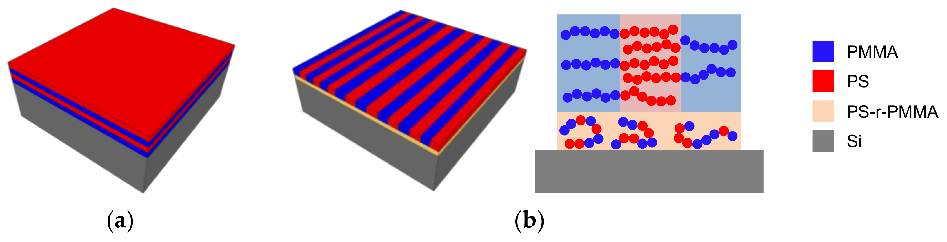
2.1. Phase Segregation in Diblock Copolymers
2.2. Self-Assembly on Thin Films
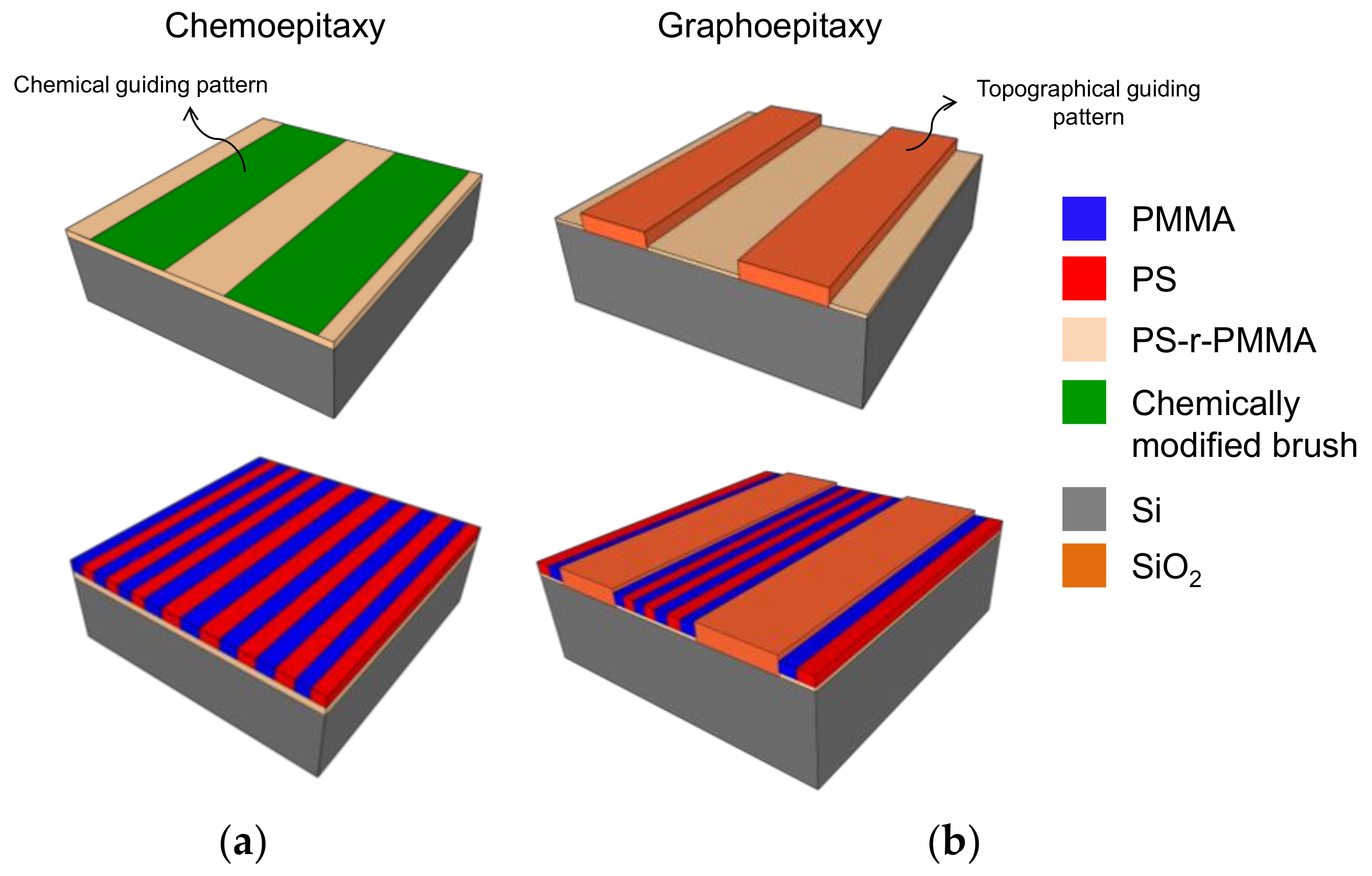
2.3. Enabling Lithography: DSA of BCPs
2.4. Present Directions
3. Block Copolymers for the Fabrication of Functional Devices
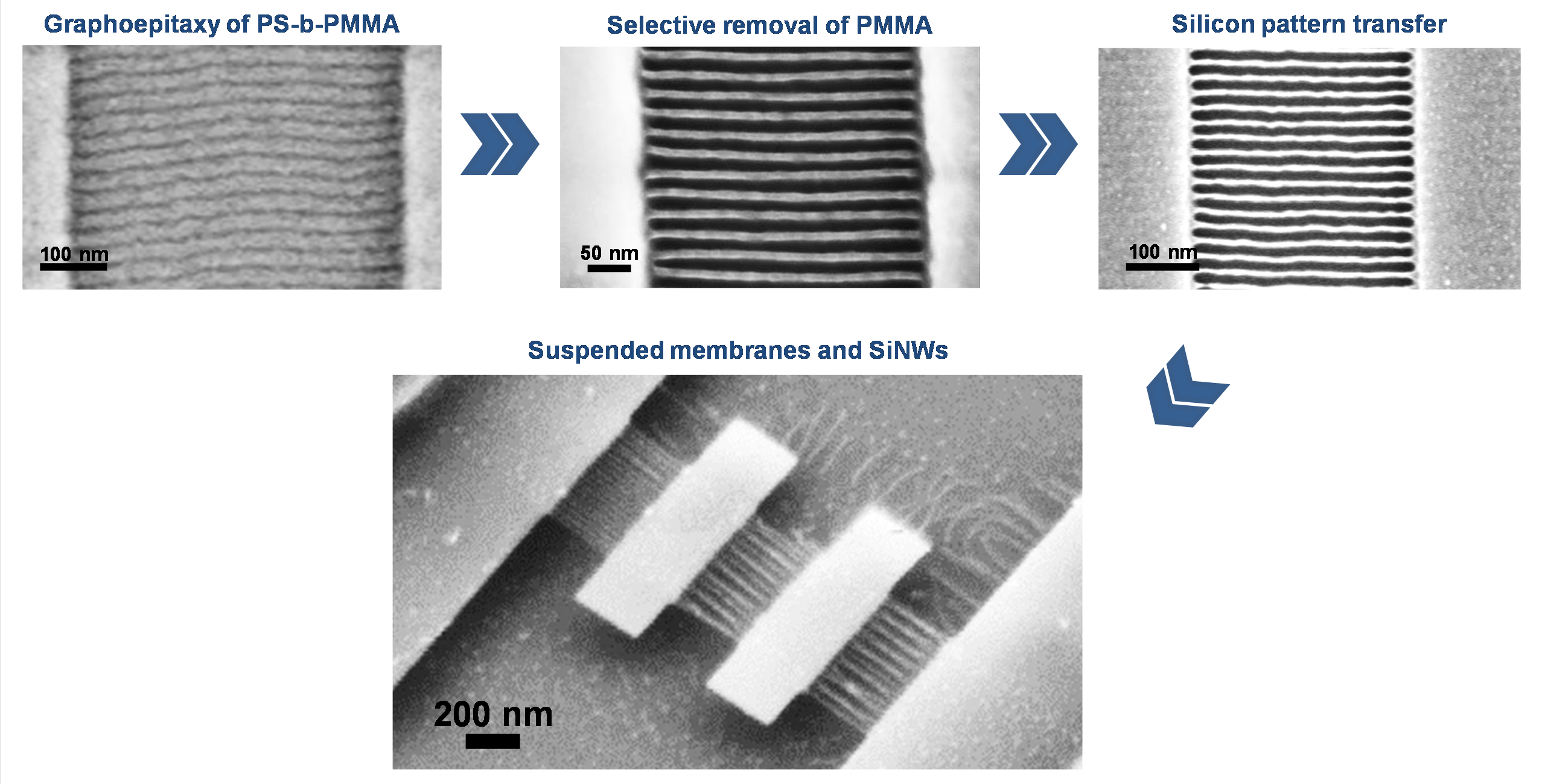
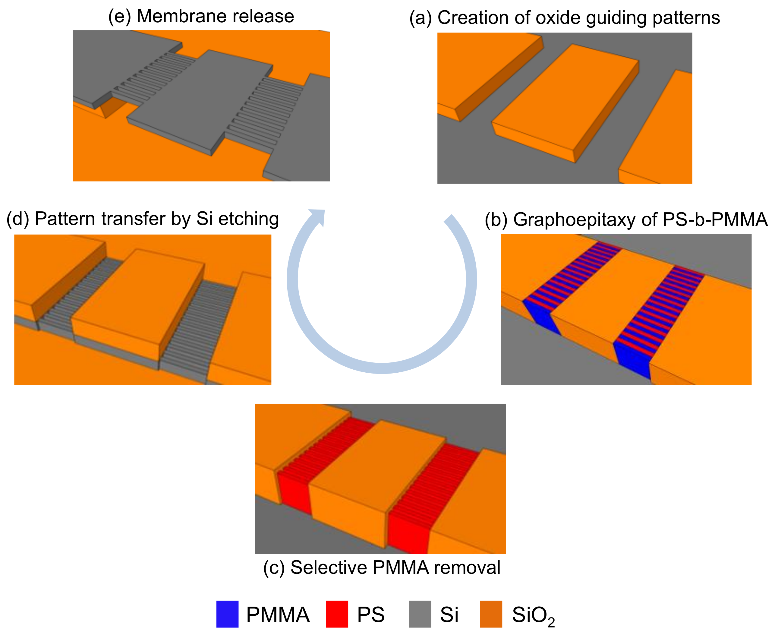
4. DSA of BCPs for the Fabrication of Nanoelectromechanical Devices
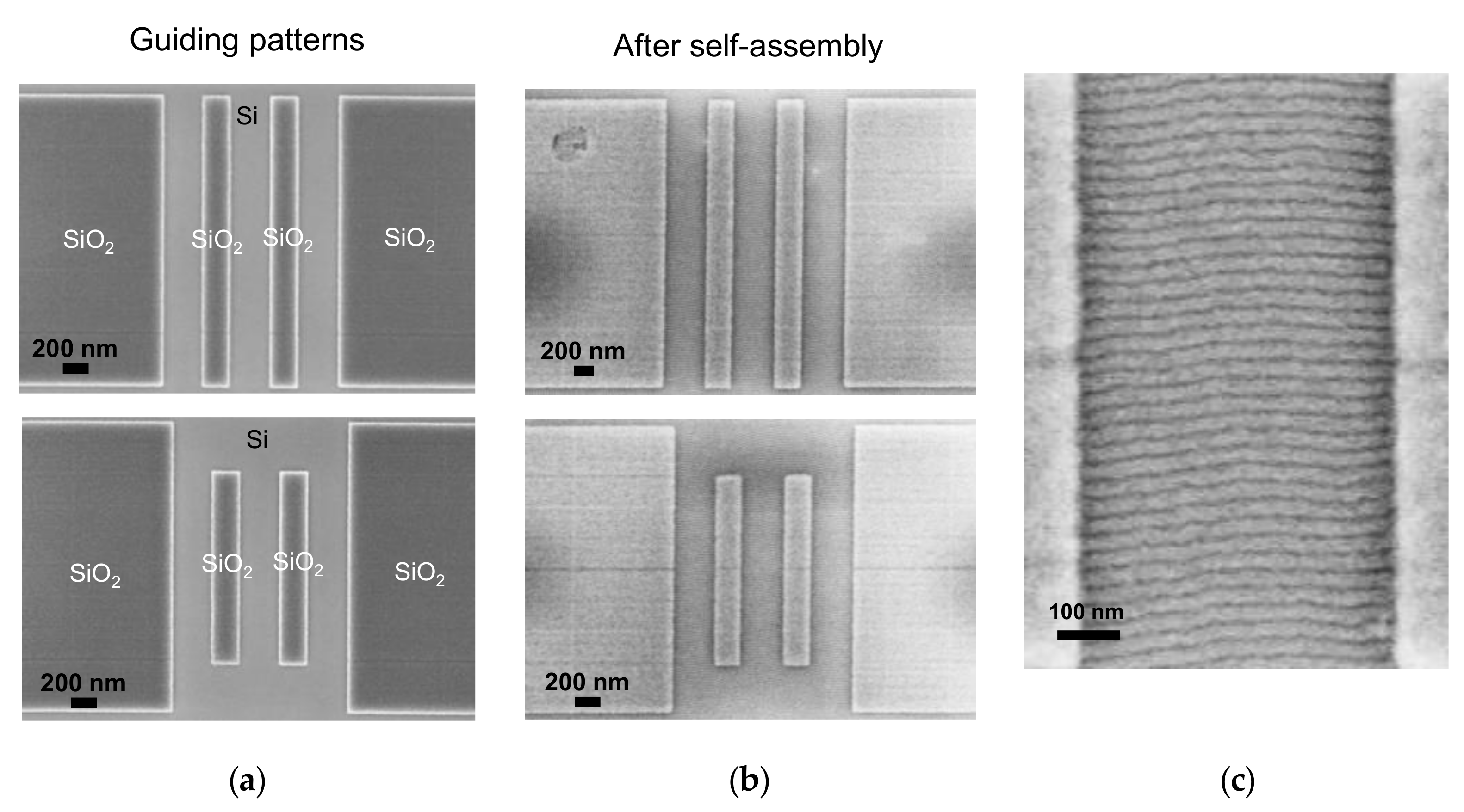
4.1. Creation of Oxide GPs by EBL
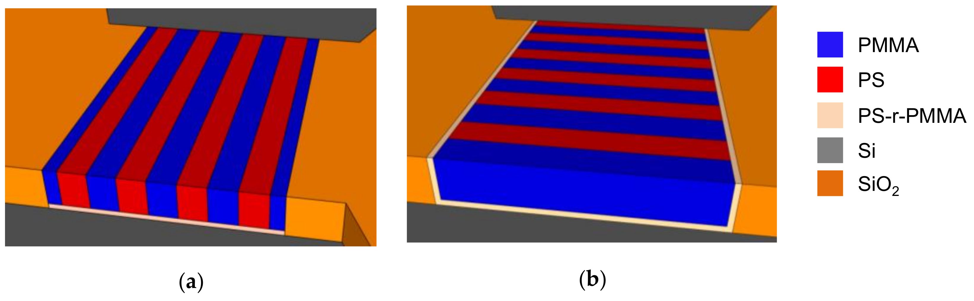
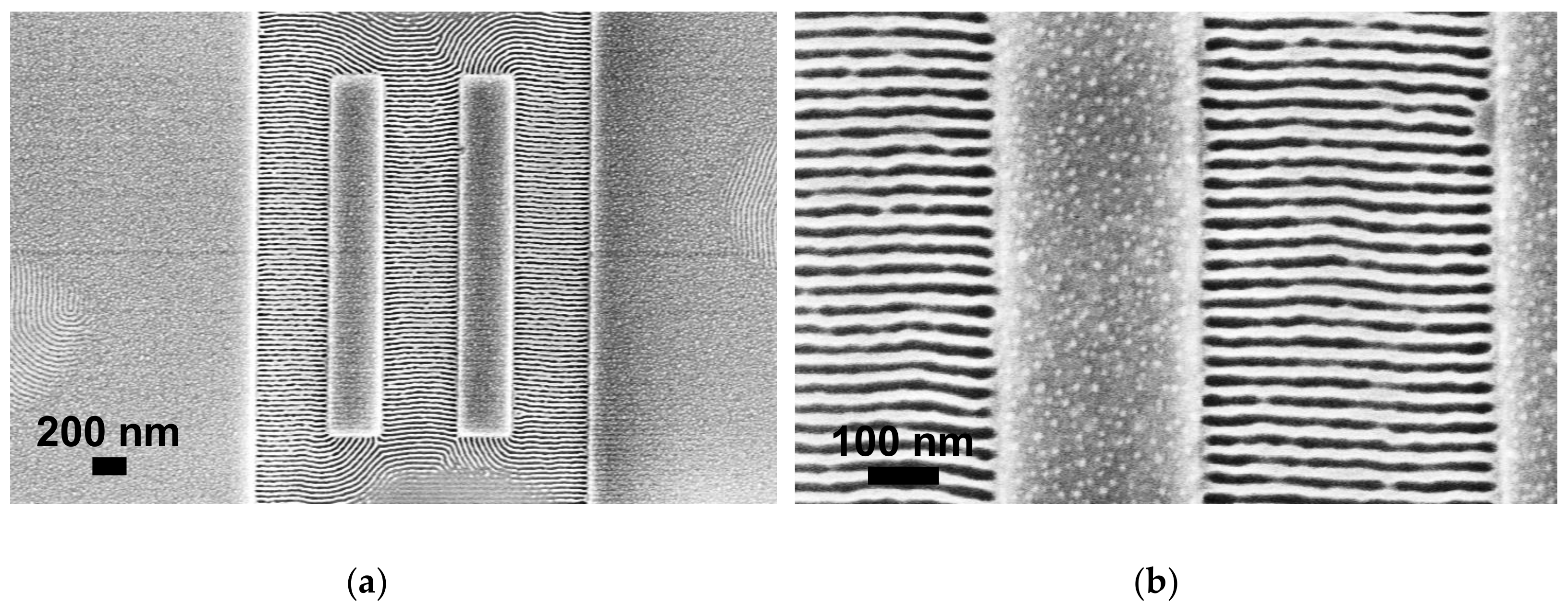
4.2. Graphoepitaxy of PS-b-PMMA
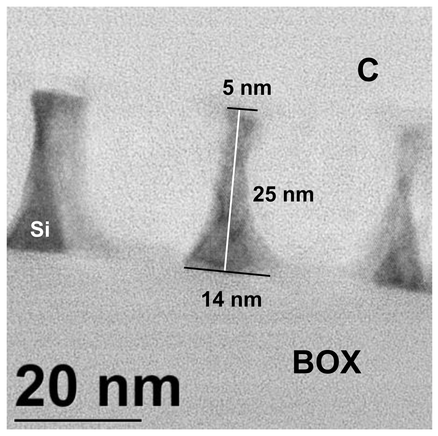
4.3. Selective PMMA Removal and Pattern Transfer
4.4. Disposal of Undesired SiNWs
4.5. Release of the Structures
5. Conclusions
Author Contributions
Funding
Acknowledgments
Conflicts of Interest
References
- Moore, G.E. Progress in digital integrated electronics Reprinted with permission. Technical Digest. International Electron Devices Meeting, IEEE, 1975, pp. 11–13. IEEE SSCS Newsl. 2006, 11, 36–37. [Google Scholar] [CrossRef]
- Anonymous. Moore’s deviation. Editorial. Nat. Nanotechnol. 2017, 12, 1105. [Google Scholar] [CrossRef] [PubMed]
- Sanders, D.P. Advances in Patterning Materials for 193 nm Immersion Lithography. Chem. Rev. 2010, 110, 321–360. [Google Scholar] [CrossRef] [PubMed]
- Hara, A.; Nishimura, E.; Kushibiki, M.; Yamauchi, S.; Natori, S.; Yabe, K.; Oyama, K.; Yaeasghi, H. Advanced self-aligned DP process development for 22-nm node and beyond. In Proceedings of the SPIE Advances in Resist Materials and Processing Technology XXVII, San Jose, CA, USA, 22–24 February 2010; Volume 7639, p. 76391T. [Google Scholar]
- Kaul, A.B. Microelectronics to Nanoelectronics: Materials, Devices & Manufacturability; CRC Press: Boca Raton, FL, USA, 2017; ISBN 978-1-351-83238-0. [Google Scholar]
- Radamson, H.H.; Zhang, Y.; He, X.; Cui, H.; Li, J.; Xiang, J.; Liu, J.; Gu, S.; Wang, G. The challenges of advanced CMOS process from 2D to 3D. Appl. Sci. 2017, 7, 1047. [Google Scholar] [CrossRef]
- Neisser, M. Patterning roadmap: 2017 prospects. Adv. Opt. Technol. 2017, 6, 143–148. [Google Scholar] [CrossRef]
- Turkot, B.; Carson, S.L.; Lio, A.; Liang, T.; Phillips, M.; McCool, B.; Stenehjem, E.; Crimmins, T.; Zhang, G.; Sivakumar, S. EUV progress toward HVM readiness. In Proceedings of the SPIE Extreme Ultraviolet (EUV) Lithography VII, San Jose, CA, USA, 22–25 February 2016; Volume 9776, p. 977602. [Google Scholar]
- Barcelo, S.; Li, Z. Nanoimprint lithography for nanodevice fabrication. Nano Converg. 2016, 3, 21. [Google Scholar] [CrossRef]
- Servin, I.; Thiam, N.A.; Pimenta-Barros, P.; Pourteau, M.-L.; Mebiene, A.-P.; Jussot, J.; Pradelles, J.; Essomba, P.; Lattard, L.; Brandt, P.; et al. Ready for multi-beam exposure at 5kV on MAPPER tool: Lithographic and process integration performances of advanced resists/stack. In Proceedings of the SPIE Alternative Lithographic Technologies VII, San Jose, CA, USA, 23–26 February 2015; Volume 9423, p. 94231C. [Google Scholar]
- Cheng, J.Y.; Rettner, C.T.; Sanders, D.P.; Kim, H.-C.; Hinsberg, W.D. Dense Self-Assembly on Sparse Chemical Patterns: Rectifying and Multiplying Lithographic Patterns Using Block Copolymers. Adv. Mater. 2008, 20, 3155–3158. [Google Scholar] [CrossRef]
- Ruiz, R.; Kang, H.; Detcheverry, F.A.; Dobisz, E.; Kercher, D.S.; Albrecht, T.R.; de Pablo, J.J.; Nealey, P.F. Density Multiplication and Improved Lithography by Directed Block Copolymer Assembly. Science 2008, 321, 936–939. [Google Scholar] [CrossRef]
- Somervell, M.; Yamauchi, T.; Okada, S.; Tomita, T.; Nishi, T.; Kawakami, S.; Muramatsu, M.; Iijima, E.; Rastogi, V.; Nakano, T.; et al. Driving DSA into volume manufacturing. In Proceedings of the SPIE Advances in Patterning Materials and Processes XXXII, San Jose, CA, USA, 23–26 February 2015; Volume 9425, p. 94250Q. [Google Scholar]
- Pan, D.Z. Directed self-assembly for advanced chips. Nat. Electron. 2018, 1, 530–531. [Google Scholar] [CrossRef]
- Mansky, P.; Haikin, P.; Thomas, E.L. Monolayer films of diblock copolymer microdomains for nanolithographic applications. J. Mater. Sci. 1995, 30, 1987–1992. [Google Scholar] [CrossRef]
- Mansky, P.; Harrison, C.K.; Chaikin, P.M.; Register, R.A.; Yao, N. Nanolithographic templates from diblock copolymer thin films. Appl. Phys. Lett. 1996, 68, 2586–2588. [Google Scholar] [CrossRef]
- Mansky, P.; Russell, T.P.; Hawker, C.J.; Pitsikalis, M.; Mays, J. Ordered Diblock Copolymer Films on Random Copolymer Brushes. Macromolecules 1997, 30, 6810–6813. [Google Scholar] [CrossRef]
- Hinsberg, W.; Cheng, J.; Kim, H.-C.; Sanders, D.P. Self-assembling materials for lithographic patterning: Overview, status, and moving forward. In Proceedings of the SPIE Alternative Lithographic Technologies II, San Jose, CA, USA, 23–25 February 2010; Volume 7637, p. 76370G. [Google Scholar]
- Herr, D.J.C. Directed block copolymer self-assembly for nanoelectronics fabrication. J. Mater. Res. 2011, 26, 122–139. [Google Scholar] [CrossRef]
- Jeong, S.-J.; Kim, J.Y.; Kim, B.H.; Moon, H.-S.; Kim, S.O. Directed self-assembly of block copolymers for next generation nanolithography. Mater. Today 2013, 16, 468–476. [Google Scholar] [CrossRef]
- Morris, M.A. Directed self-assembly of block copolymers for nanocircuitry fabrication. Microelectron. Eng. 2015, 132, 207–217. [Google Scholar] [CrossRef]
- Li, W.; Müller, M. Defects in the Self-Assembly of Block Copolymers and Their Relevance for Directed Self-Assembly. Annu. Rev. Chem. Biomol. Eng. 2015, 6, 187–216. [Google Scholar] [CrossRef]
- Bates, F.S.; Fredrickson, G.H. Block Copolymer Thermodynamics: Theory and Experiment. Annu. Rev. Phys. Chem. 1990, 41, 525–557. [Google Scholar] [CrossRef]
- Hamley, I.W. Nanostructure fabrication using block copolymers. Nanotechnology 2003, 14, R39–R54. [Google Scholar] [CrossRef]
- Black, C.T. Self-aligned self assembly of multi-nanowire silicon field effect transistors. Appl. Phys. Lett. 2005, 87, 163116. [Google Scholar] [CrossRef]
- Somervell, M.; Gronheid, R.; Hooge, J.; Nafus, K.; Delgadillo, P.R.; Thode, C.; Younkin, T.; Matsunaga, K.; Rathsack, B.; Scheer, S.; et al. Comparison of directed self-assembly integrations. In Proceedings of the SPIE Advances in Resist Materials and Processing Technology XXIX, San Jose, CA, USA, 13–15 February 2012; Volume 8325, p. 83250G. [Google Scholar]
- Somervell, M.; Yamauchi, T.; Okada, S.; Tomita, T.; Nishi, T.; Iijima, E.; Nakano, T.; Ishiguro, T.; Nagahara, S.; Iwaki, H.; et al. High-volume manufacturing equipment and processing for directed self-assembly applications. In Proceedings of the SPIE Advances in Patterning Materials and Processes XXXI, San Jose, CA, USA, 24–27 February 2014; Volume 9051, p. 90510N. [Google Scholar]
- Claveau, G.; Argoud, M.; Pimenta-Barros, P.; Chamiot-Maitral, G.; Tiron, R.; Chevalier, X.; Navarro, C. Latest evolution in a 300mm graphoepitaxy pilot line flow for L/S applications. In Proceedings of the SPIE Emerging Patterning Technologies, San Jose, CA, USA, 27 February–1 March 2017; Volume 10144, p. 1014411. [Google Scholar]
- Bai, W.; Ross, C.A. Functional nanostructured materials based on self-assembly of block copolymers. MRS Bull. 2016, 41, 100–107. [Google Scholar] [CrossRef]
- Gunkel, I. Directing Block Copolymer Self-Assembly on Patterned Substrates. Small 2018, 14, 1802872. [Google Scholar] [CrossRef] [PubMed]
- Kim, J.H.; Jin, H.M.; Yang, G.G.; Han, K.H.; Yun, T.; Shin, J.Y.; Jeong, S.-J.; Kim, S.O. Smart Nanostructured Materials based on Self-Assembly of Block Copolymers. Adv. Funct. Mater. 2020, 30, 1902049. [Google Scholar] [CrossRef]
- Bates, F.S. Polymer-polymer phase behavior. Science 1991, 251, 898–905. [Google Scholar] [CrossRef]
- Russell, T.P.; Hjelm, R.P.; Seeger, P.A. Temperature dependence of the interaction parameter of polystyrene and poly(methyl methacrylate). Macromolecules 1990, 23, 890–893. [Google Scholar] [CrossRef]
- Masson, J.-L.; Limary, R.; Green, P.F. Pattern formation and evolution in diblock copolymer thin films above the order–disorder transition. J. Chem. Phys. 2001, 114, 10963–10967. [Google Scholar] [CrossRef]
- Leibler, L. Theory of Microphase Separation in Block Copolymers. Macromolecules 1980, 13, 1602–1617. [Google Scholar] [CrossRef]
- Sinturel, C.; Bates, F.S.; Hillmyer, M.A. High χ–Low N Block Polymers: How Far Can We Go? ACS Macro Lett. 2015, 4, 1044–1050. [Google Scholar] [CrossRef]
- Hu, H.; Gopinadhan, M.; Osuji, C.O. Directed self-assembly of block copolymers: A tutorial review of strategies for enabling nanotechnology with soft matter. Soft Matter 2014, 10, 3867–3889. [Google Scholar] [CrossRef]
- Mansky, P.; Liu, Y.; Huang, E.; Russell, T.P.; Hawker, C. Controlling Polymer-Surface Interactions with Random Copolymer Brushes. Science 1997, 275, 1458–1460. [Google Scholar] [CrossRef]
- Rockford, L.; Liu, Y.; Mansky, P.; Russell, T.P.; Yoon, M.; Mochrie, S.G.J. Polymers on Nanoperiodic, Heterogeneous Surfaces. Phys. Rev. Lett. 1999, 82, 2602–2605. [Google Scholar] [CrossRef]
- Hirahara, E.; Cao, Y.; Paunescu, M.; Polishchuk, O.; Jeong, E.; Ng, E.; Shan, J.; Yin, J.; Kim, J.; Li, J.; et al. Directed Self-Assembly Materials for High Resolution beyond PS-b-PMMA. J. Photopolym. Sci. Tec. 2016, 29, 679–684. [Google Scholar] [CrossRef]
- Zhao, Y.; Sivaniah, E.; Hashimoto, T. SAXS Analysis of the Order−Disorder Transition and the Interaction Parameter of Polystyrene-block-poly(methyl methacrylate). Macromolecules 2008, 41, 9948–9951. [Google Scholar] [CrossRef]
- Perego, M.; Lupi, F.F.; Ceresoli, M.; Giammaria, T.J.; Seguini, G.; Enrico, E.; Boarino, L.; Antonioli, D.; Gianotti, V.; Sparnacci, K.; et al. Ordering dynamics in symmetric PS-b-PMMA diblock copolymer thin films during rapid thermal processing. J. Mater. Chem. C 2014, 2, 6655–6664. [Google Scholar] [CrossRef]
- Lorenzoni, M.; Evangelio, L.; Nicolet, C.; Navarro, C.; Paulo, A.S.; Murano, F.P. Nanomechanical properties of solvent cast PS and PMMA polymer blends and block co-polymers. In Proceedings of the SPIE Alternative Lithographic Technologies VII, San Jose, CA, USA, 23–26 February 2015; Volume 9423, p. 942325. [Google Scholar]
- Lorenzoni, M.; Evangelio, L.; Verhaeghe, S.; Nicolet, C.; Navarro, C.; Pérez-Murano, F. Assessing the Local Nanomechanical Properties of Self-Assembled Block Copolymer Thin Films by Peak Force Tapping. Langmuir 2015, 31, 11630–11638. [Google Scholar] [CrossRef]
- Lorenzoni, M.; Evangelio, L.; Fernández-Regúlez, M.; Nicolet, C.; Navarro, C.; Pérez-Murano, F. Sequential Infiltration of Self-Assembled Block Copolymers: A Study by Atomic Force Microscopy. J. Phys. Chem. C 2017, 121, 3078–3086. [Google Scholar] [CrossRef]
- Black, C.T.; Forrey, C.; Yager, K.G. Thickness-dependence of block copolymer coarsening kinetics. Soft Matter 2017, 13, 3275–3283. [Google Scholar] [CrossRef] [PubMed]
- Fernández-Regúlez, M.; Pinto-Gómez, C.; Perez-Murano, F. Synchrotron Radiation for the Understanding of Block Copolymer Self-assembly. J. Photopolym. Sci. Tec. 2019, 32, 423–427. [Google Scholar] [CrossRef]
- Fernández-Regúlez, M.; Solano, E.; Evangelio, L.; Gottlieb, S.; Pinto-Gómez, C.; Rius, G.; Fraxedas, J.; Gutiérrez-Fernández, E.; Nogales, A.; García-Gutiérrez, M.C.; et al. Self-assembly of block copolymers under non-isothermal annealing conditions as revealed by grazing-incidence small-angle X-ray scattering. J. Synchrotron Rad. 2020, 27, 1278–1288. [Google Scholar] [CrossRef]
- Suh, H.S.; Dudash, V.; Lorusso, G.; Mack, C. Roughness study on line and space patterning with chemo-epitaxy directed self-assembly. In Proceedings of the SPIE Advances in Patterning Materials and Processes XXXVII, San Jose, CA, USA, 24–26 February 2020; Volume 11326, p. 113260X. [Google Scholar]
- Albert, J.N.L.; Epps, T.H. Self-assembly of block copolymer thin films. Mater. Today 2010, 13, 24–33. [Google Scholar] [CrossRef]
- Huang, E.; Russell, T.P.; Harrison, C.; Chaikin, P.M.; Register, R.A.; Hawker, C.J.; Mays, J. Using Surface Active Random Copolymers to Control the Domain Orientation in Diblock Copolymer Thin Films. Macromolecules 1998, 31, 7641–7650. [Google Scholar] [CrossRef]
- Sinturel, C.; Vayer, M.; Morris, M.; Hillmyer, M.A. Solvent Vapor Annealing of Block Polymer Thin Films. Macromolecules 2013, 46, 5399–5415. [Google Scholar] [CrossRef]
- Tiron, R.; Chevalier, X.; Gaugiran, S.; Pradelles, J.; Fontaine, H.; Couderc, C.; Pain, L.; Navarro, C.; Chevolleau, T.; Cunge, G.; et al. Pattern density multiplication by direct self assembly of block copolymers: Toward 300 mm CMOS requirements. In Proceedings of the SPIE Alternative Lithographic Technologies IV, San Jose, CA, USA, 13–16 February 2012; Volume 8323, p. 83230O. [Google Scholar]
- Wang, S.; Deng, W.; Seow, Y.A.; Chen, B.; Lin, Q.Y. Study of Line-Space Pitch Multiplication Using Graphoepitaxy Directed Self-Assembly for Semiconductor Applications. J. Electron. Mater. 2017, 46, 4405–4413. [Google Scholar] [CrossRef]
- Black, C.T.; Ruiz, R.; Breyta, G.; Cheng, J.Y.; Colburn, M.E.; Guarini, K.W.; Kim, H.-C.; Zhang, Y. Polymer self assembly in semiconductor microelectronics. IBM J. Res. Dev. 2007, 51, 605–633. [Google Scholar] [CrossRef]
- Oria, L.; de Luzuriaga, A.R.; Chevalier, X.; Alduncin, J.A.; Mecerreyes, D.; Tiron, R.; Gaugiran, S.; Perez-Murano, F. Guided self-assembly of block-copolymer for CMOS technology: A comparative study between grapho-epitaxy and surface chemical modification. In Proceedings of the SPIE Alternative Lithographic Technologies III, San Jose, CA, USA, 1–3 March 2011; Volume 7970, p. 79700P. [Google Scholar]
- Kim, S.O.; Solak, H.H.; Stoykovich, M.P.; Ferrier, N.J.; de Pablo, J.J.; Nealey, P.F. Epitaxial self-assembly of block copolymers on lithographically defined nanopatterned substrates. Nature 2003, 424, 411–414. [Google Scholar] [CrossRef] [PubMed]
- Cheng, J.Y.; Sanders, D.P.; Truong, H.D.; Harrer, S.; Friz, A.; Holmes, S.; Colburn, M.; Hinsberg, W.D. Simple and versatile methods to integrate directed self-assembly with optical lithography using a polarity-switched photoresist. ACS Nano 2010, 4, 4815–4823. [Google Scholar] [CrossRef]
- Oria, L.; de Luzuriaga, A.R.; Alduncín, J.A.; Pérez-Murano, F. Block co-polymer guided self-assembly by surface chemical modification: Optimization of multiple patterning process and pattern transfer. In Proceedings of the SPIE Alternative Lithographic Technologies IV, San Jose, CA, USA, 13–16 February 2012; Volume 8323, p. 832327. [Google Scholar]
- Oria, L.; de Luzuriaga, A.R.; Alduncin, J.A.; Perez-Murano, F. Polystyrene as a brush layer for directed self-assembly of block co-polymers. Microelectron. Eng. 2013, 110, 234–240. [Google Scholar] [CrossRef]
- Evangelio, L.; Gramazio, F.; Lorenzoni, M.; Gorgoi, M.; Espinosa, F.M.; García, R.; Pérez-Murano, F.; Fraxedas, J. Identifying the nature of surface chemical modification for directed self-assembly of block copolymers. Beilstein J. Nanotechnol. 2017, 8, 1972–1981. [Google Scholar] [CrossRef] [PubMed]
- Navarro, C.; Nicolet, C.; Ariura, F.; Chevalier, X.; Xu, K.; Hockey, M.A.; Mumtaz, M.; Fleury, G.; Hadziioannou, G.; Legrain, A.; et al. Recent Achievements in Sub-10 nm DSA Lithography for Line/Space Patterning. J. Photopolym. Sci. Tec. 2017, 30, 69–75. [Google Scholar] [CrossRef]
- Evangelio, L.; Fernández-Regúlez, M.; Fraxedas, J.; Müller, M.; Pérez-Murano, F. Role of Penetrability into a Brush-Coated Surface in Directed Self-Assembly of Block Copolymers. ACS Appl. Mater. Inter. 2018, 11, 3571–3581. [Google Scholar] [CrossRef]
- Evangelio, L.; Fernández-Regúlez, M.; Borrisé, X.; Lorenzoni, M.; Fraxedas, J.; Pérez-Murano, F. Creation of guiding patterns for directed self-assembly of block copolymers by resistless direct e-beam exposure. J. Micro-Nanolith. MEM 2015, 14, 033511. [Google Scholar] [CrossRef]
- Fernández-Regúlez, M.; Evangelio, L.; Lorenzoni, M.; Fraxedas, J.; Pérez-Murano, F. Sub-10 nm Resistless Nanolithography for Directed Self-Assembly of Block Copolymers. ACS Appl. Mater. Inter. 2014, 6, 21596–21602. [Google Scholar] [CrossRef]
- Gottlieb, S.; Lorenzoni, M.; Evangelio, L.; Fernández-Regúlez, M.; Ryu, Y.K.; Rawlings, C.; Spieser, M.; Knoll, A.W.; Perez-Murano, F. Thermal scanning probe lithography for the directed self-assembly of block copolymers. Nanotechnology 2017, 28, 175301. [Google Scholar] [CrossRef] [PubMed]
- Gottlieb, S.; Fernández-Regúlez, M.; Lorenzoni, M.; Evangelio, L.; Perez-Murano, F. Grain-Boundary-Induced Alignment of Block Copolymer Thin Films. Nanomaterials 2020, 10, 103. [Google Scholar] [CrossRef] [PubMed]
- Segalman, R.A.; Yokoyama, H.; Kramer, E.J. Graphoepitaxy of Spherical Domain Block Copolymer Films. Adv. Mater. 2001, 13, 1152–1155. [Google Scholar] [CrossRef]
- Black, C.T. Polymer Self-Assembly as a Novel Extension to Optical Lithography. ACS Nano 2007, 1, 147–150. [Google Scholar] [CrossRef]
- Claveau, G.; Quemere, P.; Argoud, M.; Hazart, J.; Barros, P.P.; Sarrazin, A.; Posseme, N.; Tiron, R.; Chevalier, X.; Nicolet, C.; et al. Surface affinity role in graphoepitaxy of lamellar block copolymers. In Proceedings of the SPIE Advances in Patterning Materials and Processes XXXIII, San Jose, CA, USA, 22–25 February 2016; Volume 9779, p. 97791F. [Google Scholar]
- Borah, D.; Cummins, C.; Rasappa, S.; Senthamaraikannan, R.; Salaun, M.; Zelsmann, M.; Liontos, G.; Ntetsikas, K.; Avgeropoulos, A.; Morris, M.A. Nanopatterning via Self-Assembly of a Lamellar-Forming Polystyrene-block-Poly(dimethylsiloxane) Diblock Copolymer on Topographical Substrates Fabricated by Nanoimprint Lithography. Nanomaterials 2018, 8, 32. [Google Scholar] [CrossRef] [PubMed]
- Gottlieb, S.; Rösner, B.; Evangelio, L.; Fernández-Regúlez, M.; Nogales, A.; García-Gutiérrez, M.C.; Keller, F.T.; Fraxedas, J.; Ezquerra, A.T.; David, C.; et al. Self-assembly morphology of block copolymers in sub-10 nm topographical guiding patterns. Mol. Syst. Des. Eng. 2019, 4, 175–185. [Google Scholar] [CrossRef]
- Cheng, J.Y.; Zhang, F.; Chuang, V.P.; Mayes, A.M.; Ross, C.A. Self-Assembled One-Dimensional Nanostructure Arrays. Nano Lett. 2006, 6, 2099–2103. [Google Scholar] [CrossRef] [PubMed]
- Tavakkoli, K.G.A.; Gotrik, K.W.; Hannon, A.F.; Alexander-Katz, A.; Ross, C.A.; Berggren, K.K. Templating Three-Dimensional Self-Assembled Structures in Bilayer Block Copolymer Films. Science 2012, 336, 1294–1298. [Google Scholar] [CrossRef] [PubMed]
- Wan, L.; Ruiz, R.; Gao, H.; Patel, K.C.; Albrecht, T.R.; Yin, J.; Kim, J.; Cao, Y.; Lin, G. The Limits of Lamellae-Forming PS-b-PMMA Block Copolymers for Lithography. ACS Nano 2015, 9, 7506–7514. [Google Scholar] [CrossRef] [PubMed]
- Yoshida, K.; Tanaka, S.; Yamamoto, T.; Tajima, K.; Borsali, R.; Isono, T.; Satoh, T. Chain-End Functionalization with a Saccharide for 10 nm Microphase Separation: “Classical” PS-b-PMMA versus PS-b-PMMA-Saccharide. Macromolecules 2018, 51, 8870–8877. [Google Scholar] [CrossRef]
- Yoshida, K.; Yamamoto, T.; Tajima, K.; Isono, T.; Satoh, T. Installing a functional group into the inactive ω-chain end of PMMA and PS-b-PMMA by terminal-selective transesterification. Polym. Chem. 2019, 10, 3390–3398. [Google Scholar] [CrossRef]
- Sunday, D.F.; Chen, X.; Albrecht, T.R.; Nowak, D.; Delgadillo, P.R.; Dazai, T.; Miyagi, K.; Maehashi, T.; Yamazaki, A.; Nealey, P.F.; et al. Influence of Additives on the Interfacial Width and Line Edge Roughness in Block Copolymer Lithography. Chem. Mater. 2020, 32, 2399–2407. [Google Scholar] [CrossRef]
- Tsai, H.; Miyazoe, H.; Vora, A.; Magbitang, T.; Arellano, N.; Liu, C.-C.; Maher, M.J.; Durand, W.J.; Dawes, S.J.; Bucchignano, J.J.; et al. High chi block copolymer DSA to improve pattern quality for FinFET device fabrication. In Proceedings of the SPIE Advances in Patterning Materials and Processes XXXIII, San Jose, CA, USA, 22–25 February 2016; Volume 9779, p. 977910. [Google Scholar]
- Lane, A.P.; Yang, X.; Maher, M.J.; Blachut, G.; Asano, Y.; Someya, Y.; Mallavarapu, A.; Sirard, S.M.; Ellison, C.J.; Willson, C.G. Directed Self-Assembly and Pattern Transfer of Five Nanometer Block Copolymer Lamellae. ACS Nano 2017, 11, 7656–7665. [Google Scholar] [CrossRef] [PubMed]
- Asakawa, K.; Hiraoka, T.; Hieda, H.; Sakurai, M.; Kamata, Y.; Naito, K. Nano-Patterning for Patterned Media using Block-Copolymer. J. Photopolym. Sci. Tec. 2002, 15, 465–470. [Google Scholar] [CrossRef]
- Cushen, J.D.; Otsuka, I.; Bates, C.M.; Halila, S.; Fort, S.; Rochas, C.; Easley, J.A.; Rausch, E.L.; Thio, A.; Borsali, R.; et al. Oligosaccharide/silicon-containing block copolymers with 5 nm features for lithographic applications. ACS Nano 2012, 6, 3424–3433. [Google Scholar] [CrossRef]
- Cushen, J.; Wan, L.; Blachut, G.; Maher, M.J.; Albrecht, T.R.; Ellison, C.J.; Willson, C.G.; Ruiz, R. Double-Patterned Sidewall Directed Self-Assembly and Pattern Transfer of Sub-10 nm PTMSS-b-PMOST. ACS Appl. Mater. Interfaces 2015, 7, 13476–13483. [Google Scholar] [CrossRef]
- Bates, C.M.; Seshimo, T.; Maher, M.J.; Durand, W.J.; Cushen, J.D.; Dean, L.M.; Blachut, G.; Ellison, C.J.; Willson, C.G. Polarity-Switching Top Coats Enable Orientation of Sub–10-nm Block Copolymer Domains. Science 2012, 338, 775–779. [Google Scholar] [CrossRef]
- Blachut, G.; Sirard, S.M.; Maher, M.J.; Asano, Y.; Someya, Y.; Lane, A.P.; Durand, W.J.; Bates, C.M.; Dinhobl, A.M.; Gronheid, R.; et al. A Hybrid Chemo-/Grapho-Epitaxial Alignment Strategy for Defect Reduction in Sub-10 nm Directed Self-Assembly of Silicon-Containing Block Copolymers. Chem. Mater. 2016, 28, 8951–8961. [Google Scholar] [CrossRef]
- Xiong, S.; Chapuis, Y.-A.; Wan, L.; Gao, H.; Li, X.; Ruiz, R.; Nealey, P.F. Directed self-assembly of high-chi block copolymer for nano fabrication of bit patterned media via solvent annealing. Nanotechnology 2016, 27, 415601. [Google Scholar] [CrossRef]
- Xiong, S.; Wan, L.; Ishida, Y.; Chapuis, Y.-A.; Craig, G.S.W.; Ruiz, R.; Nealey, P.F. Directed Self-Assembly of Triblock Copolymer on Chemical Patterns for Sub-10-nm Nanofabrication via Solvent Annealing. ACS Nano 2016, 10, 7855–7865. [Google Scholar] [CrossRef] [PubMed]
- Yang, G.-W.; Wu, G.-P.; Chen, X.; Xiong, S.; Arges, C.G.; Ji, S.; Nealey, P.F.; Lu, X.-B.; Darensbourg, D.J.; Xu, Z.-K. Directed Self-Assembly of Polystyrene-b-poly(propylene carbonate) on Chemical Patterns via Thermal Annealing for Next Generation Lithography. Nano Lett. 2017, 17, 1233–1239. [Google Scholar] [CrossRef] [PubMed]
- Maher, M.J.; Bates, C.M.; Blachut, G.; Sirard, S.; Self, J.L.; Carlson, M.C.; Dean, L.M.; Cushen, J.D.; Durand, W.J.; Hayes, C.O.; et al. Interfacial Design for Block Copolymer Thin Films. Chem. Mater. 2014, 26, 1471–1479. [Google Scholar] [CrossRef]
- Borah, D.; Ozmen, M.; Rasappa, S.; Shaw, M.T.; Holmes, J.D.; Morris, M.A. Molecularly Functionalized Silicon Substrates for Orientation Control of the Microphase Separation of PS-b-PMMA and PS-b-PDMS Block Copolymer Systems. Langmuir 2013, 29, 2809–2820. [Google Scholar] [CrossRef]
- Durand, W.J.; Blachut, G.; Maher, M.J.; Sirard, S.; Tein, S.; Carlson, M.C.; Asano, Y.; Zhou, S.X.; Lane, A.P.; Bates, C.M.; et al. Design of high-χ block copolymers for lithography. J. Polym. Sci. A Polym. Chem. 2015, 53, 344–352. [Google Scholar] [CrossRef]
- Yamada, Y.; Ito, K.; Miura, A.; Harada, M.; Matsunaga, T.; Kato, Y.; Matsui, T.; Iizuka, H.; Wakayama, H. Perpendicular SiO2 cylinders fabricated from a self-assembled block copolymer as an adaptable platform. Eur. Polym. J. 2018, 107, 96–104. [Google Scholar] [CrossRef]
- Albalak, R.J.; Capel, M.S.; Thomas, E.L. Solvent swelling of roll-cast triblock copolymer films. Polymer 1998, 39, 1647–1656. [Google Scholar] [CrossRef]
- Jung, Y.S.; Ross, C.A. Orientation-Controlled Self-Assembled Nanolithography Using a Polystyrene−Polydimethylsiloxane Block Copolymer. Nano Lett. 2007, 7, 2046–2050. [Google Scholar] [CrossRef]
- Cummins, C.; Kelly, R.A.; Gangnaik, A.; Georgiev, Y.M.; Petkov, N.; Holmes, J.D.; Morris, M.A. Solvent vapor annealing of block copolymers in confined topographies: Commensurability considerations for nanolithography. Macromol. Rapid Commun. 2015, 36, 762–767. [Google Scholar] [CrossRef]
- Seshimo, T.; Bates, C.M.; Dean, L.M.; Cushen, J.D.; Durand, W.J.; Maher, M.J.; Ellison, C.J.; Willson, C.G. Block copolymer orientation control using a top-coat surface treatment. J. Photopolym. Sci. Tec. 2012, 25, 125–130. [Google Scholar] [CrossRef]
- Ober, C.K. Directed self-assembly: A dress code for block copolymers. Nat. Nanotechnol. 2017, 12, 507–508. [Google Scholar] [CrossRef] [PubMed]
- Delgadillo, P.A.R.; Gronheid, R.; Thode, C.J.; Wu, H.; Cao, Y.; Somervell, M.; Nafus, K.; Nealey, P.F. All track directed self-assembly of block copolymers: Process flow and origin of defects. In Proceedings of the SPIE Alternative Lithographic Technologies IV, San Jose, CA, USA, 13–16 February 2012; Volume 8323, p. 83230D. [Google Scholar]
- Delgadillo, P.R.; Harukawa, R.; Suri, M.; Durant, S.; Cross, A.; Nagaswami, V.R.; Heuvel, D.V.D.; Gronheid, R.; Nealey, P. Defect source analysis of directed self-assembly process (DSA of DSA). In Proceedings of the SPIE Alternative Lithographic Technologies V, San Jose, CA, USA, 25–28 February 2013; Volume 8680, p. 86800L. [Google Scholar]
- Gronheid, R.; Singh, A.; Younkin, T.R.; Delgadillo, P.R.; Nealey, P.; Chan, B.T.; Nafus, K.; Negreira, A.R.; Somervell, M. Rectification of EUV-patterned contact holes using directed self-assembly. In Proceedings of the SPIE Advances in Resist Materials and Processing Technology XXX, San Jose, CA, USA, 25–27 February 2013; Volume 8682, p. 86820A. [Google Scholar]
- Ito, C.; Durant, S.; Lange, S.; Harukawa, R.; Miyagi, T.; Nagaswami, V.; Delgadillo, P.R.; Gronheid, R.; Nealey, P. Inspection of directed self-assembly defects. In Proceedings of the SPIE Alternative Lithographic Technologies VI, San Jose, CA, USA, 24–27 February 2014; Volume 9049, p. 90492D. [Google Scholar]
- Muramatsu, M.; Nishi, T.; You, G.; Ido, Y.; Kitano, T. Pattern defect reduction for chemo-epitaxy DSA process. In Proceedings of the SPIE Advances in Patterning Materials and Processes XXXVI, San Jose, CA, USA, 25–28 February 2019; Gronheid, R., Sanders, D.P., Eds.; SPIE: Bellingham, WA, USA, 2019. [Google Scholar]
- Doise, J.; Koh, J.H.; Kim, J.Y.; Zhu, Q.; Kinoshita, N.; Suh, H.S.; Delgadillo, P.R.; Vandenberghe, G.; Willson, C.G.; Ellison, C.J. Strategies for Increasing the Rate of Defect Annihilation in the Directed Self-Assembly of High-χ Block Copolymers. ACS Appl. Mater. Interfaces 2019, 11, 48419–48427. [Google Scholar] [CrossRef] [PubMed]
- Li, J.; Rincon-Delgadillo, P.A.; Suh, H.S.; Mannaert, G.; Nealey, P.F. Kinetic approach to defect reduction in directed self-assembly. J. Micro-Nanolith. MEM 2019, 18, 043502. [Google Scholar] [CrossRef]
- Doise, J.; Mannaert, G.; Suh, H.S.; Rincon, P.; Koh, J.H.; Kim, J.Y.; Zhu, Q.; Vandenberghe, G.; Willson, C.G.; Ellison, C.J. Defect mitigation in sub-20nm patterning with high-chi, silicon-containing block copolymers. In Proceedings of the SPIE Advances in Patterning Materials and Processes XXXVI, San Jose, CA, USA, 25–28 February 2019; Volume 10960, p. 109600Y. [Google Scholar]
- Kim, Y.C.; Shin, T.J.; Hur, S.-M.; Kwon, S.J.; Kim, S.Y. Shear-solvo defect annihilation of diblock copolymer thin films over a large area. Sci. Adv. 2019, 5, eaaw3974. [Google Scholar] [CrossRef]
- Muramatsu, M.; Nishi, T.; Ido, Y.; Kitano, T. Defect mitigation of chemo-epitaxy DSA patterns. In Proceedings of the SPIE Advances in Patterning Materials and Processes XXXVII, San Jose, CA, USA, 24–26 February 2020; Volume 11326, p. 113260Y. [Google Scholar]
- Liu, C.-C.; Franke, E.; Mignot, Y.; Xie, R.; Yeung, C.W.; Zhang, J.; Chi, C.; Zhang, C.; Farrell, R.; Lai, K.; et al. Directed self-assembly of block copolymers for 7 nanometre FinFET technology and beyond. Nat. Electron. 2018, 1, 562–569. [Google Scholar] [CrossRef]
- Jeong, S.-J.; Kim, J.E.; Moon, H.-S.; Kim, B.H.; Kim, S.M.; Kim, J.B.; Kim, S.O. Soft Graphoepitaxy of Block Copolymer Assembly with Disposable Photoresist Confinement. Nano Lett. 2009, 9, 2300–2305. [Google Scholar] [CrossRef]
- Kim, J.; Wan, J.; Miyazaki, S.; Yin, J.; Cao, Y.; Her, Y.J.; Wu, H.; Shan, J.; Kurosawa, K.; Lin, G. The SMART Process for Directed Block Co-Polymer Self-Assembly. J. Photopolym. Sci. Tec. 2013, 26, 573–579. [Google Scholar] [CrossRef][Green Version]
- Liu, C.-C.; Lie, F.L.; Rastogi, V.; Franke, E.; Mohanty, N.; Farrell, R.; Tsai, H.; Lai, K.; Ozlem, M.; Cho, W.; et al. Fin formation using graphoepitaxy DSA for FinFET device fabrication. In Proceedings of the SPIE Alternative Lithographic Technologies VII, San Jose, CA, USA, 23–26 February 2015; Volume 9423, p. 94230S. [Google Scholar]
- Singh, A.; Chan, B.T.; Parnell, D.; Wu, H.; Yin, J.; Cao, Y.; Gronheid, R. Patterning sub-25nm half-pitch hexagonal arrays of contact holes with chemo-epitaxial DSA guided by ArFi pre-patterns. In Proceedings of the SPIE Advances in Patterning Materials and Processes XXXII, San Jose, CA, USA, 23–26 February 2015; Volume 9425, p. 94250X. [Google Scholar]
- Seino, Y.; Kasahara, Y.; Sato, H.; Kobayashi, K.; Kubota, H.; Minegishi, S.; Miyagi, K.; Kanai, H.; Kodera, K.; Kihara, N.; et al. Directed self-assembly lithography using coordinated line epitaxy (COOL) process. In Proceedings of the SPIE Alternative Lithographic Technologies VII, San Jose, CA, USA, 23–26 February 2015; p. 942316. [Google Scholar]
- Liu, C.-C.; Han, E.; Onses, M.S.; Thode, C.J.; Ji, S.; Gopalan, P.; Nealey, P.F. Fabrication of Lithographically Defined Chemically Patterned Polymer Brushes and Mats. Macromolecules 2011, 44, 1876–1885. [Google Scholar] [CrossRef]
- Liu, C.-C.; Ramírez-Hernández, A.; Han, E.; Craig, G.S.W.; Tada, Y.; Yoshida, H.; Kang, H.; Ji, S.; Gopalan, P.; de Pablo, J.J.; et al. Chemical Patterns for Directed Self-Assembly of Lamellae-Forming Block Copolymers with Density Multiplication of Features. Macromolecules 2013, 46, 1415–1424. [Google Scholar] [CrossRef]
- Sayan, S.; Marzook, T.; Chan, B.T.; Vandenbroeck, N.; Singh, A.; Laidler, D.; Sanchez, E.A.; Leray, P.; Delgadillo, P.R.; Gronheid, R.; et al. Toward sub-20nm pitch Fin patterning and integration with DSA. In Proceedings of the SPIE Advances in Patterning Materials and Processes XXXIII, San Jose, CA, USA, 22–25 February 2016; Volume 9779, p. 97790R. [Google Scholar]
- Liu, C.-C.; Estrada-Raygoza, I.C.; Abdallah, J.; Holmes, S.; Yin, Y.; Schepis, A.; Cicoria, M.; Hetzer, D.; Tsai, H.; Guillorn, M.; et al. Directed self-assembly process implementation in a 300mm pilot line environment. In Proceedings of the SPIE Alternative Lithographic Technologies V, San Jose, CA, USA, 25–28 February 2013; Volume 8680, p. 86801G. [Google Scholar]
- Russell, T.P.; Coulon, G.; Deline, V.R.; Miller, D.C. Characteristics of the surface-induced orientation for symmetric diblock PS/PMMA copolymers. Macromolecules 1989, 22, 4600–4606. [Google Scholar] [CrossRef]
- Park, S.-M.; Stoykovich, M.P.; Ruiz, R.; Zhang, Y.; Black, C.T.; Nealey, P.F. Directed Assembly of Lamellae- Forming Block Copolymers by Using Chemically and Topographically Patterned Substrates. Adv. Mater. 2007, 19, 607–611. [Google Scholar] [CrossRef]
- Tsai, H.; Pitera, J.W.; Miyazoe, H.; Bangsaruntip, S.; Engelmann, S.U.; Liu, C.-C.; Cheng, J.Y.; Bucchignano, J.J.; Klaus, D.P.; Joseph, E.A.; et al. Two-Dimensional Pattern Formation Using Graphoepitaxy of PS-b-PMMA Block Copolymers for Advanced FinFET Device and Circuit Fabrication. ACS Nano 2014, 8, 5227–5232. [Google Scholar] [CrossRef] [PubMed]
- Gottlieb, S.; Kazazis, D.; Mochi, I.; Evangelio, L.; Fernández-Regúlez, M.; Ekinci, Y.; Perez-Murano, F. Nano-confinement of block copolymers in high accuracy topographical guiding patterns: Modelling the emergence of defectivity due to incommensurability. Soft Matter 2018, 14, 6799–6808. [Google Scholar] [CrossRef]
- Tiron, R.; Gharbi, A.; Argoud, M.; Chevalier, X.; Belledent, J.; Pimenta Barros, P.; Navarro, C.; Cunge, G.; Pain, L.; Asai, M.; et al. The potential of block copolymer’s directed self-assembly for contact hole shrink and contact multiplication. In Proceedings of the SPIE Alternative Lithographic Technologies V, San Jose, CA, USA, 25–28 February 2013; Volume 8680, p. 868012. [Google Scholar]
- Tiron, R.; Gharbi, A.; Barros, P.P.; Bouanani, S.; Lapeyre, C.; Bos, S.; Fouquet, A.; Hazart, J.; Chevalier, X.; Argoud, M.; et al. Template affinity role in CH shrink by DSA planarization. In Proceedings of the SPIE Alternative Lithographic Technologies VII, San Jose, CA, USA, 23–26 February 2015; Volume 9423, p. 942317. [Google Scholar]
- Servin, I.; Tiron, R.; Gharbi, A.; Argoud, M.; Jullian, K.; Chamiot-Maitral, G.; Barros, P.P.; Chevalier, X.; Belledent, J.; Bossy, X.; et al. Contact hole shrink by directed self-assembly: Process integration and stability monitored on 300 mm pilot line. Jpn. J. Appl. Phys. 2014, 53, 06JC05. [Google Scholar] [CrossRef]
- Gharbi, A.; Tiron, R.; Argoud, M.; Chamiot-Maitral, G.; Fouquet, A.; Lapeyre, C.; Barros, P.P.; Delachat, F.; Bos, S.; Bouanani, S.; et al. Process highlights to enhance directed self-assembly contact patterning performances. J. Micro/Nanolith. MEMS MOEMS 2016, 15, 043503. [Google Scholar] [CrossRef]
- Liu, C.-C.; Franke, E.; Mignot, Y.; LeFevre, S.; Sieg, S.; Chi, C.; Meli, L.; Parnell, D.; Schmidt, K.; Sanchez, M.; et al. DSA patterning options for logics and memory applications. In Proceedings of the SPIE Advances in Patterning Materials and Processes XXXIV, San Jose, CA, USA, 27 February–3 March 2017; Volume 10146, p. 1014603. [Google Scholar]
- Bruce, R.L.; Fraczak, G.; Papalia, J.M.; Tsai, H.; BrightSky, M.; Miyazoe, H.; Zhu, Y.; Engelmann, S.U.; Lung, H.-L.; Masuda, T.; et al. Directed self-assembly patterning strategies for phase change memory applications. In Proceedings of the SPIE Advanced Etch Technology for Nanopatterning VI, San Jose, CA, USA, 27 February–1 March 2017; Volume 10149, p. 101490J. [Google Scholar]
- Tseng, Y.-C.; Peng, Q.; Ocola, L.E.; Elam, J.W.; Darling, S.B. Enhanced Block Copolymer Lithography Using Sequential Infiltration Synthesis. J. Phys. Chem. C 2011, 115, 17725–17729. [Google Scholar] [CrossRef]
- Elam, J.W.; Biswas, M.; Darling, S.B.; Yanguas-Gil, A.; Emery, J.D.; Martinson, A.B.F.; Nealey, P.F.; Segal-Peretz, T.; Peng, Q.; Winterstein, J.; et al. New Insights into Sequential Infiltration Synthesis. ECS Trans. 2015, 69, 147–157. [Google Scholar] [CrossRef] [PubMed]
- Gharbi, A.; Pimenta-Barros, P.; Saouaf, O.; Reynaud, G.; Pain, L.; Tiron, R.; Navarro, C.; Nicolet, C.; Cayrefourcq, I.; Perego, M.; et al. Pillars fabrication by DSA lithography: Material and process options. In Proceedings of the SPIE Advances in Patterning Materials and Processes XXXV, San Jose, CA, USA, 26 February–1 March 2018; Volume 10586, p. 105860Q. [Google Scholar]
- Amat, E.; del Moral, A.; Fernández-Regúlez, M.; Evangelio, L.; Lorenzoni, M.; Gharbi, A.; Rademaker, G.; Pourteau, M.-L.; Tiron, R.; Bausells, J.; et al. Exploring Strategies to Contact 3D Nano-Pillars. Nanomaterials 2020, 10, 716. [Google Scholar] [CrossRef]
- Ruiz, R.; Dobisz, E.; Albrecht, T.R. Rectangular Patterns Using Block Copolymer Directed Assembly for High Bit Aspect Ratio Patterned Media. ACS Nano 2011, 5, 79–84. [Google Scholar] [CrossRef]
- Park, W.I.; You, B.K.; Mun, B.H.; Seo, H.K.; Lee, J.Y.; Hosaka, S.; Yin, Y.; Ross, C.A.; Lee, K.J.; Jung, Y.S. Self-Assembled Incorporation of Modulated Block Copolymer Nanostructures in Phase-Change Memory for Switching Power Reduction. ACS Nano 2013, 7, 2651–2658. [Google Scholar] [CrossRef]
- Griffiths, R.A.; Williams, A.; Oakland, C.; Roberts, J.; Vijayaraghavan, A.; Thomson, T. Directed self-assembly of block copolymers for use in bit patterned media fabrication. J. Phys. D Appl. Phys. 2013, 46, 503001. [Google Scholar] [CrossRef]
- You, B.K.; Park, W.I.; Kim, J.M.; Park, K.-I.; Seo, H.K.; Lee, J.Y.; Jung, Y.S.; Lee, K.J. Reliable Control of Filament Formation in Resistive Memories by Self-Assembled Nanoinsulators Derived from a Block Copolymer. ACS Nano 2014, 8, 9492–9502. [Google Scholar] [CrossRef] [PubMed]
- Stefik, M.; Guldin, S.; Vignolini, S.; Wiesner, U.; Steiner, U. Block copolymer self-assembly for nanophotonics. Chem. Soc. Rev. 2015, 44, 5076–5091. [Google Scholar] [CrossRef] [PubMed]
- Jin, H.M.; Kim, J.Y.; Heo, M.; Jeong, S.-J.; Kim, B.H.; Cha, S.K.; Han, K.H.; Kim, J.H.; Yang, G.G.; Shin, J.; et al. Ultralarge Area Sub-10 nm Plasmonic Nanogap Array by Block Copolymer Self-Assembly for Reliable High-Sensitivity SERS. ACS Appl. Mater. Inter. 2018, 10, 44660–44667. [Google Scholar] [CrossRef] [PubMed]
- Rasappa, S.; Schulte, L.; Ndoni, S.; Niemi, T. Directed self-assembly of a high-chi block copolymer for the fabrication of optical nanoresonators. Nanoscale 2018, 10, 18306–18314. [Google Scholar] [CrossRef] [PubMed]
- Rasappa, S.; Borah, D.; Faulkner, C.C.; Lutz, T.; Shaw, M.T.; Holmes, J.D.; Morris, M.A. Fabrication of a sub-10 nm silicon nanowire based ethanol sensor using block copolymer lithography. Nanotechnology 2013, 24, 065503. [Google Scholar] [CrossRef] [PubMed]
- Kim, B.H.; Kim, J.Y.; Jeong, S.-J.; Hwang, J.O.; Lee, D.H.; Shin, D.O.; Choi, S.-Y.; Kim, S.O. Surface Energy Modification by Spin-Cast, Large-Area Graphene Film for Block Copolymer Lithography. ACS Nano 2010, 4, 5464–5470. [Google Scholar] [CrossRef] [PubMed]
- Kim, J.Y.; Kim, B.H.; Hwang, J.O.; Jeong, S.-J.; Shin, D.O.; Mun, J.H.; Choi, Y.J.; Jin, H.M.; Kim, S.O. Flexible and Transferrable Self-Assembled Nanopatterning on Chemically Modified Graphene. Adv. Mater. 2013, 25, 1331–1335. [Google Scholar] [CrossRef]
- Arias-Zapata, J.; Garnier, J.D.; Mehedi, H.; Legrain, A.; Salem, B.; Cunge, G.; Zelsmann, M. Engineering Self-Assembly of a High-χ Block Copolymer for Large-Area Fabrication of Transistors Based on Functional Graphene Nanoribbon Arrays. Chem. Mater. 2019, 31, 3154–3162. [Google Scholar] [CrossRef]
- Chang, T.-H.; Xiong, S.; Jacobberger, R.M.; Mikael, S.; Suh, H.S.; Liu, C.-C.; Geng, D.; Wang, X.; Arnold, M.S.; Ma, Z.; et al. Directed self-assembly of block copolymer films on atomically-thin graphene chemical patterns. Sci. Rep. 2016, 6, 31407. [Google Scholar] [CrossRef]
- Yang, S.Y.; Park, J.; Yoon, J.; Ree, M.; Jang, S.K.; Kim, J.K. Virus Filtration Membranes Prepared from Nanoporous Block Copolymers with Good Dimensional Stability under High Pressures and Excellent Solvent Resistance. Adv. Funct. Mater. 2008, 18, 1371–1377. [Google Scholar] [CrossRef]
- Jackson, E.A.; Hillmyer, M.A. Nanoporous Membranes Derived from Block Copolymers: From Drug Delivery to Water Filtration. ACS Nano 2010, 4, 3548–3553. [Google Scholar] [CrossRef] [PubMed]
- Li, X.; Fustin, C.-A.; Lefèvre, N.; Gohy, J.-F.; Feyter, S.D.; Baerdemaeker, J.D.; Egger, W.; Vankelecom, I.F.J. Ordered nanoporous membranes based on diblock copolymers with high chemical stability and tunable separation properties. J. Mater. Chem. 2010, 20, 4333–4339. [Google Scholar] [CrossRef]
- Phillip, W.A.; Dorin, R.M.; Werner, J.; Hoek, E.M.V.; Wiesner, U.; Elimelech, M. Tuning structure and properties of graded triblock terpolymer-based mesoporous and hybrid films. Nano Lett. 2011, 11, 2892–2900. [Google Scholar] [CrossRef] [PubMed]
- Lundy, R.; Flynn, S.P.; Cummins, C.; Kelleher, S.M.; Collins, M.N.; Dalton, E.; Daniels, S.; Morris, M.; Enright, R. Nanoporous membrane production via block copolymer lithography for high heat dissipation systems. In Proceedings of the 15th IEEE Intersociety Conference on Thermal and Thermomechanical Phenomena in Electronic Systems, Las Vegas, NV, USA, 31 May–3 June 2016; pp. 1267–1272. [Google Scholar]
- Shen, L.; He, C.; Qiu, J.; Lee, S.-M.; Kalita, A.; Cronin, S.B.; Stoykovich, M.P.; Yoon, J. Nanostructured Silicon Photocathodes for Solar Water Splitting Patterned by the Self-Assembly of Lamellar Block Copolymers. ACS Appl. Mater. Interfaces 2015, 7, 26043–26049. [Google Scholar] [CrossRef]
- Adak, D.; Ghosh, S.; Chakraborty, P.; Srivatsa, K.M.K.; Mondal, A.; Saha, H.; Mukherjee, R.; Bhattacharyya, R. Non lithographic block copolymer directed self-assembled and plasma treated self-cleaning transparent coating for photovoltaic modules and other solar energy devices. Sol. Energy Mater. Sol. Cells 2018, 188, 127–139. [Google Scholar] [CrossRef]
- Werner, J.G.; Rodríguez-Calero, G.G.; Abruña, H.D.; Wiesner, U. Block copolymer derived 3-D interpenetrating multifunctional gyroidal nanohybrids for electrical energy storage. Energy Environ. Sci. 2018, 11, 1261–1270. [Google Scholar] [CrossRef]
- Zou, Y.; Zhou, X.; Ma, J.; Yang, X.; Deng, Y. Recent advances in amphiphilic block copolymer templated mesoporous metal-based materials: Assembly engineering and applications. Chem. Soc. Rev. 2020, 49, 1173–1208. [Google Scholar] [CrossRef]
- Cummins, C.; Lundy, R.; Walsh, J.J.; Ponsinet, V.; Fleury, G.; Morris, M.A. Enabling future nanomanufacturing through block copolymer self-assembly: A review. Nano Today 2020, 35, 100936. [Google Scholar] [CrossRef]
- Tritschler, U.; Pearce, S.; Gwyther, J.; Whittell, G.R.; Manners, I. 50th Anniversary Perspective: Functional Nanoparticles from the Solution Self-Assembly of Block Copolymers. Macromolecules 2017, 50, 3439–3463. [Google Scholar] [CrossRef]
- Checco, A.; Rahman, A.; Black, C.T. Robust Superhydrophobicity in Large-Area Nanostructured Surfaces Defined by Block-Copolymer Self Assembly. Adv. Mater. 2014, 26, 886–891. [Google Scholar] [CrossRef] [PubMed]
- Rahman, A.; Ashraf, A.; Xin, H.; Tong, X.; Sutter, P.; Eisaman, M.D.; Black, C.T. Sub-50-nm self-assembled nanotextures for enhanced broadband antireflection in silicon solar cells. Nat. Commun. 2015, 6, 1–6. [Google Scholar] [CrossRef]
- Di Mauro, A.E.; Villone, V.; Ingrosso, C.; Corricelli, M.; Oria, L.; Pérez-Murano, F.; Agostiano, A.; Striccoli, M.; Curri, M.L. H-bonding driven assembly of colloidal Au nanoparticles on nanostructured poly(styrene-b-ethylene oxide) block copolymer templates. J. Mater. Sci. 2014, 49, 5246–5255. [Google Scholar] [CrossRef]
- Ekinci, K.L.; Roukes, M.L. Nanoelectromechanical systems. Rev. Sci. Instrum. 2005, 76, 061101. [Google Scholar] [CrossRef]
- Ekinci, K.L.; Huang, X.M.H.; Roukes, M.L. Ultrasensitive nanoelectromechanical mass detection. Appl. Phys. Lett. 2004, 84, 4469–4471. [Google Scholar] [CrossRef]
- Ekinci, K.L.; Yang, Y.T.; Roukes, M.L. Ultimate limits to inertial mass sensing based upon nanoelectromechanical systems. J. Appl. Phys. 2004, 95, 2682–2689. [Google Scholar] [CrossRef]
- Gil-Santos, E.; Ramos, D.; Martínez, J.; Fernández-Regúlez, M.; García, R.; San Paulo, Á.; Calleja, M.; Tamayo, J. Nanomechanical mass sensing and stiffness spectrometry based on two-dimensional vibrations of resonant nanowires. Nat. Nanotechnol. 2010, 5, 641–645. [Google Scholar] [CrossRef]
- Eom, K.; Park, H.S.; Yoon, D.S.; Kwon, T. Nanomechanical resonators and their applications in biological/chemical detection: Nanomechanics principles. Phys. Rep. 2011, 503, 115–163. [Google Scholar] [CrossRef]
- Fernandez-Regulez, M.; Sansa, M.; Serra-Garcia, M.; Gil-Santos, E.; Tamayo, J.; Perez-Murano, F.; Paulo, A.S. Horizontally patterned Si nanowire growth for nanomechanical devices. Nanotechnology 2013, 24, 095303. [Google Scholar] [CrossRef]
- Sansa, M.; Fernández-Regúlez, M.; Llobet, J.; San Paulo, Á.; Pérez-Murano, F. High-sensitivity linear piezoresistive transduction for nanomechanical beam resonators. Nat. Commun. 2014, 5, 1–9. [Google Scholar] [CrossRef]
- Dasgupta, N.P.; Sun, J.; Liu, C.; Brittman, S.; Andrews, S.C.; Lim, J.; Gao, H.; Yan, R.; Yang, P. 25th Anniversary Article: Semiconductor Nanowires – Synthesis, Characterization, and Applications. Adv. Mater. 2014, 26, 2137–2184. [Google Scholar] [CrossRef]
- Arcamone, J.; Rius, G.; Abadal, G.; Teva, J.; Barniol, N.; Pérez-Murano, F. Micro/nanomechanical resonators for distributed mass sensing with capacitive detection. Microelectron. Eng. 2006, 83, 1216–1220. [Google Scholar] [CrossRef]
- Schmid, S.; Villanueva, L.G.; Roukes, M.L. Fundamentals of Nanomechanical Resonators; Springer International Publishing: Basel, Switzerland, 2016; ISBN 978-3-319-28689-1. [Google Scholar]
- Mohammad, M.A.; Dew, S.K.; Evoy, S.; Stepanova, M. Fabrication of sub-10nm silicon carbon nitride resonators using a hydrogen silsesquioxane mask patterned by electron beam lithography. Microelectron. Eng. 2011, 88, 2338–2341. [Google Scholar] [CrossRef]
- Ryu, D.Y.; Shin, K.; Drockenmuller, E.; Hawker, C.J.; Russell, T.P. A Generalized Approach to the Modification of Solid Surfaces. Science 2005, 308, 236–239. [Google Scholar] [CrossRef] [PubMed]
- Han, E.; Stuen, K.O.; La, Y.-H.; Nealey, P.F.; Gopalan, P. Effect of Composition of Substrate-Modifying Random Copolymers on the Orientation of Symmetric and Asymmetric Diblock Copolymer Domains. Macromolecules 2008, 41, 9090–9097. [Google Scholar] [CrossRef]
- Boufnichel, M.; Aachboun, S.; Lefaucheux, P.; Ranson, P. Profile control of high aspect ratio trenches of silicon. II. Study of the mechanisms responsible for local bowing formation and elimination of this effect. J. Vac. Sci. Technol. B 2003, 21, 267–273. [Google Scholar] [CrossRef]
- Lee, J.-K.; Jang, I.-Y.; Lee, S.-H.; Kim, C.-K.; Moon, S.H. Mechanism of Sidewall Necking and Bowing in the Plasma Etching of High Aspect-Ratio Contact Holes. J. Electrochem. Soc. 2010, 157, D142. [Google Scholar] [CrossRef]
- Borah, D.; Shaw, M.T.; Rasappa, S.; Farrell, R.A.; O’Mahony, C.; Faulkner, C.M.; Bosea, M.; Gleeson, P.; Holmes, J.D.; Morris, M.A. Plasma etch technologies for the development of ultra-small feature size transistor devices. J. Phys. D Appl. Phys. 2011, 44, 174012. [Google Scholar] [CrossRef]


Publisher’s Note: MDPI stays neutral with regard to jurisdictional claims in published maps and institutional affiliations. |
© 2020 by the authors. Licensee MDPI, Basel, Switzerland. This article is an open access article distributed under the terms and conditions of the Creative Commons Attribution (CC BY) license (http://creativecommons.org/licenses/by/4.0/).
Share and Cite
Pinto-Gómez, C.; Pérez-Murano, F.; Bausells, J.; Villanueva, L.G.; Fernández-Regúlez, M. Directed Self-Assembly of Block Copolymers for the Fabrication of Functional Devices. Polymers 2020, 12, 2432. https://doi.org/10.3390/polym12102432
Pinto-Gómez C, Pérez-Murano F, Bausells J, Villanueva LG, Fernández-Regúlez M. Directed Self-Assembly of Block Copolymers for the Fabrication of Functional Devices. Polymers. 2020; 12(10):2432. https://doi.org/10.3390/polym12102432
Chicago/Turabian StylePinto-Gómez, Christian, Francesc Pérez-Murano, Joan Bausells, Luis Guillermo Villanueva, and Marta Fernández-Regúlez. 2020. "Directed Self-Assembly of Block Copolymers for the Fabrication of Functional Devices" Polymers 12, no. 10: 2432. https://doi.org/10.3390/polym12102432
APA StylePinto-Gómez, C., Pérez-Murano, F., Bausells, J., Villanueva, L. G., & Fernández-Regúlez, M. (2020). Directed Self-Assembly of Block Copolymers for the Fabrication of Functional Devices. Polymers, 12(10), 2432. https://doi.org/10.3390/polym12102432