Characterization and Application of PVDF and Its Copolymer Films Prepared by Spin-Coating and Langmuir–Blodgett Method

Abstract

1. Introduction
2. Preparation
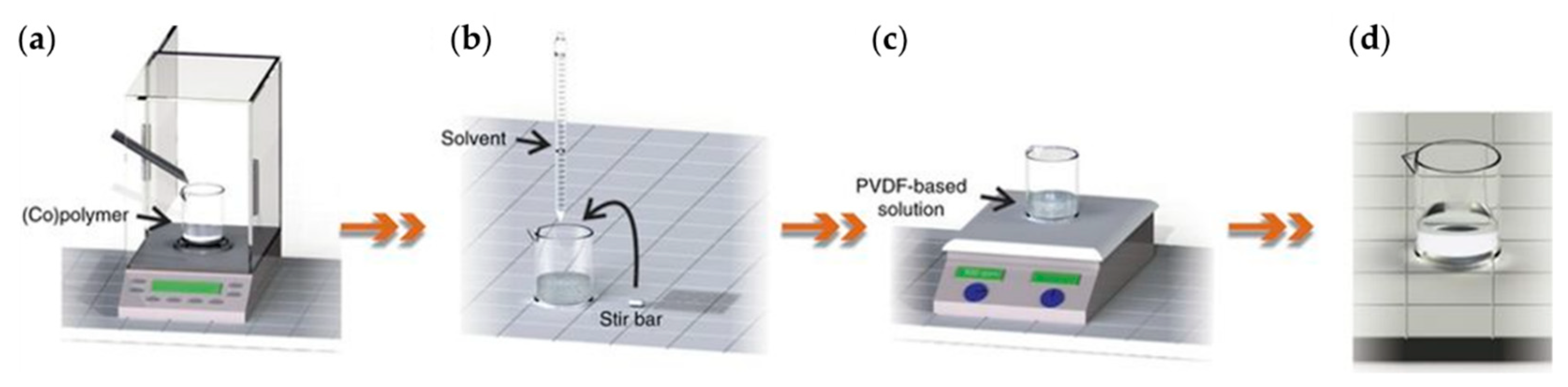
2.1. Spin-Coating Method
2.2. Langmuir–Blodgett Deposition
3. Characterization
3.1. Fourier Transform Infrared (FTIR)
3.2. XRD
3.3. Ferroelectric Capacitor
3.4. Scanning Probe Microscope (SPM)
4. Physical Theory
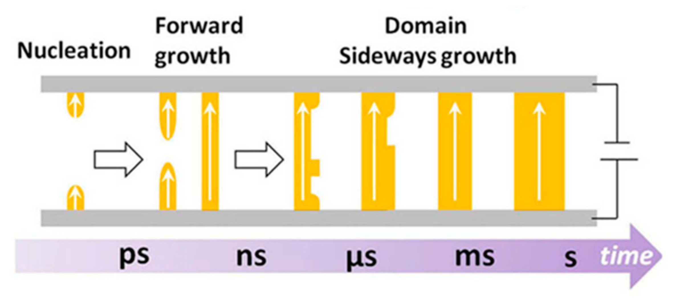
4.1. KAI Model
4.2. NLS Model
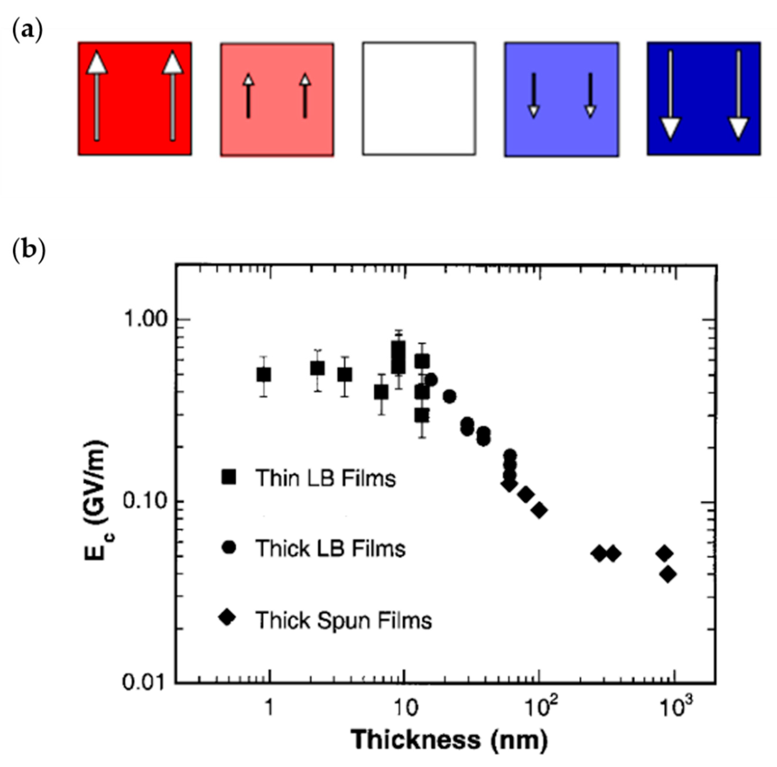
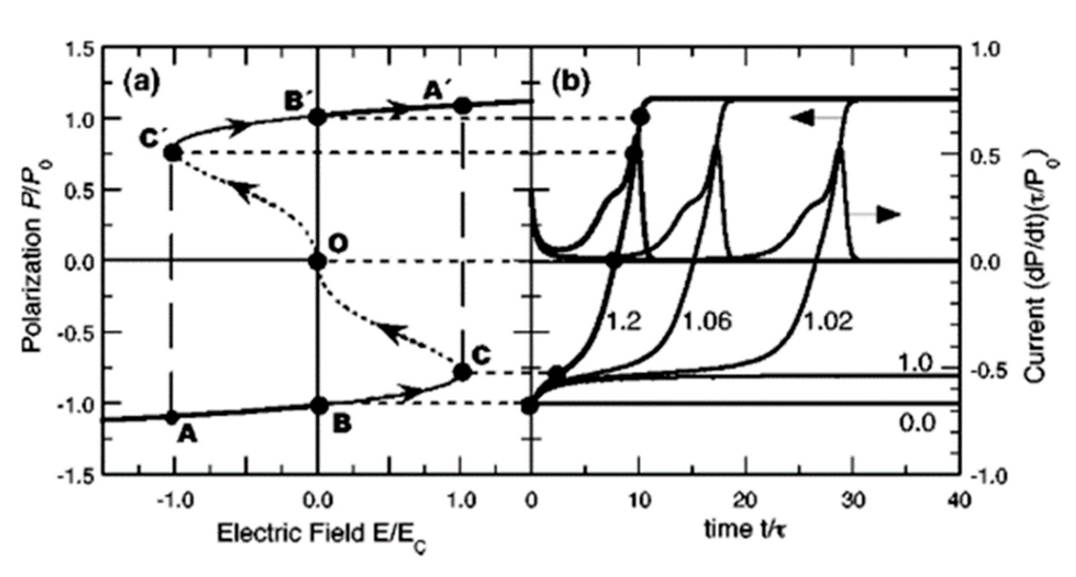
4.3. Intrinsic Switching
5. Application
5.1. Nonvolatile Memory
5.2. Memristive Devices and Artificial Neutral Synapse
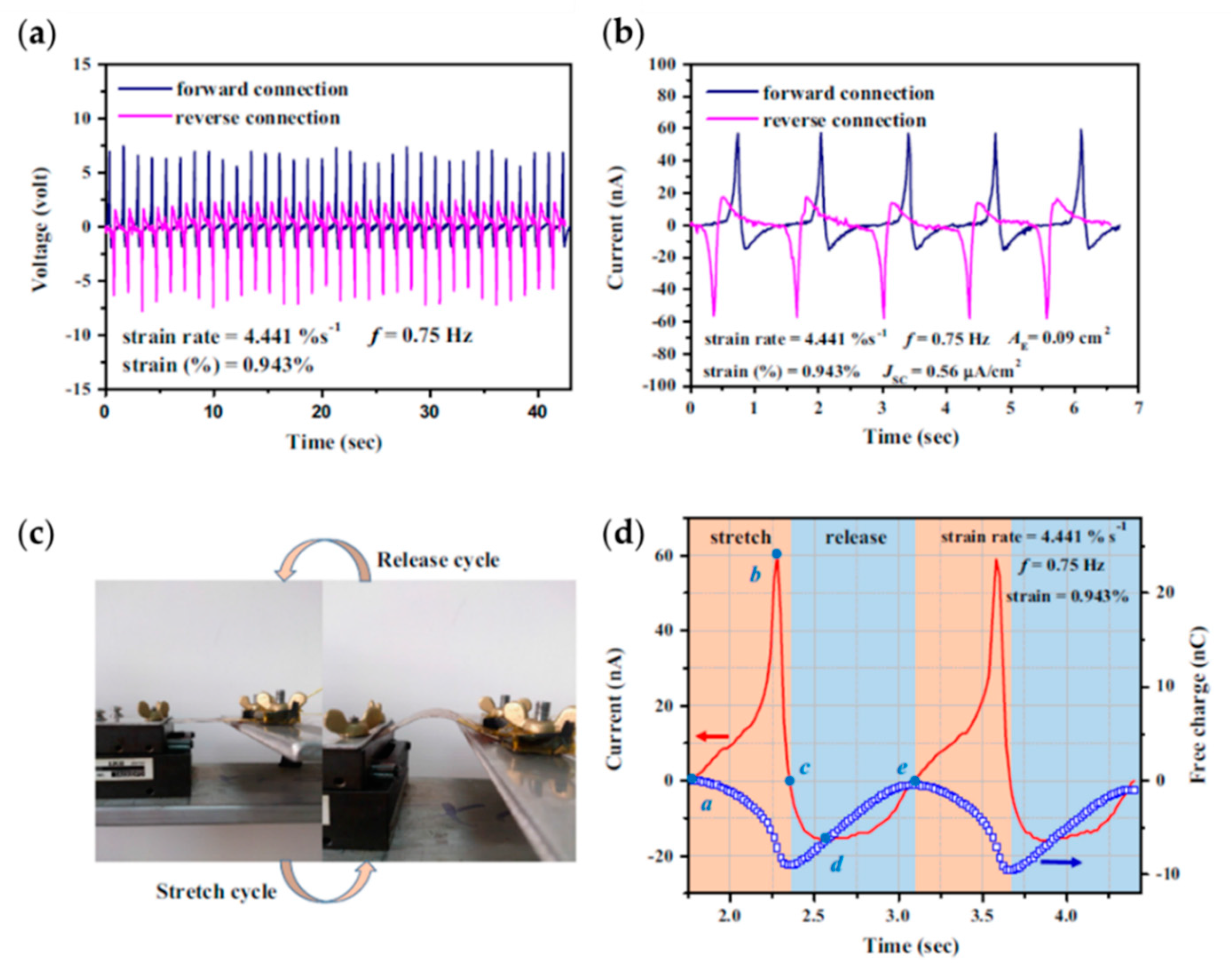
5.3. Flexible Electronic Devices
5.4. Medical Applications
6. Outlooks
7. Conclusions
Author Contributions
Funding
Conflicts of Interest
References
- Ishiwara, H.; Okuyama, M.; Arimoto, Y. Ferroelectric Random Access Memories: Fundamentals and Applications; Springer: Berlin/Heidelberg, Germany, 2004. [Google Scholar]
- Park, B.-E.; Ishiwara, H.; Okuyama, M.; Sakai, S.; Yoon, S.-M. Ferroelectric-Gate Field Effect Transistor Memories: Device Physics and Applications; Springer Science+Business Media: Dordrecht, The Netherlands, 2016. [Google Scholar]
- Setter, N.; Damjanovic, D.; Eng, L.; Fox, G.; Gevorgian, S.; Hong, S.; Kingon, A.; Kohlstedt, H.; Park, N.Y.; Stephenson, G.B.; et al. Ferroelectric thin films: Review of materials, properties, and applications. J. Appl. Phys. 2006, 100, 051606. [Google Scholar] [CrossRef]
- Ruan, L.; Yao, X.; Chang, Y.; Zhou, L.; Qin, G.; Zhang, X. Properties and applications of the β phase poly(vinylidene fluoride). Polymers 2018, 10, 228. [Google Scholar] [CrossRef] [PubMed]
- Tian, B.B.; Wang, J.L.; Fusil, S.; Liu, Y.; Zhao, X.L.; Sun, S.; Shen, H.; Lin, T.; Sun, J.L.; Duan, C.G.; et al. Tunnel electroresistance through organic ferroelectrics. Nat. Commun. 2016, 7, 11502. [Google Scholar] [CrossRef] [PubMed]
- Mathur, S.C.; Scheinbeim, J.I.; Newman, B.A. Piezoelectric properties and ferroelectric hysteresis effects in uniaxially stretched nylon-11 films. J. Appl. Phys. 1984, 56, 2419–2425. [Google Scholar] [CrossRef]
- Horiuchi, S.; Tokunaga, Y.; Giovannetti, G.; Picozzi, S.; Itoh, H.; Shimano, R.; Kumai, R.; Tokura, Y. Above-room-temperature ferroelectricity in a single-component molecular crystal. Nature 2010, 463, 789–792. [Google Scholar] [CrossRef]
- Fu, D.W.; Cai, H.L.; Liu, Y.; Ye, Q.; Zhang, W.; Zhang, Y.; Chen, X.Y.; Giovannetti, G.; Capone, M.; Li, J.; et al. Diisopropylammonium bromide is a high-temperature molecular ferroelectric crystal. Science 2013, 339, 425–428. [Google Scholar] [CrossRef]
- Tian, B.; Liu, L.; Yan, M.; Wang, J.; Zhao, Q.; Zhong, N.; Xiang, P.; Sun, L.; Peng, H.; Shen, H.; et al. A robust artificial synapse based on organic ferroelectric polymer. Adv. Electron. Mater. 2019, 5, 1800600. [Google Scholar] [CrossRef]
- Furukawa, T. Ferroelectric properties of vinylidene fluoride copolymers. Ph. Transit. 1989, 18, 143–211. [Google Scholar] [CrossRef]
- Nalwa, H.S. Handbook of Thin Film Materials; Academic Press: Cambridge, MA, USA, 2002. [Google Scholar]
- Koseki, Y.; Aimi, K.; Ando, S. Crystalline structure and molecular mobility of PVDF chains in PVDF/PMMA blend films analyzed by solid-state 19F MAS NMR spectroscopy. Polym. J. 2012, 44, 757–763. [Google Scholar] [CrossRef]
- Nalwa, H.S. Ferroelectric Polymers: Chemistry, Physics, and Applications; Marcel Dekker, Inc.: New York, NY, USA, 1995. [Google Scholar]
- Wang, Z.-Y.; Fan, H.-Q.; Su, K.-H.; Wen, Z.-Y. Structure and piezoelectric properties of poly(vinylidene fluoride) studied by density functional theory. Polymer 2006, 47, 7988–7996. [Google Scholar] [CrossRef]
- Wang, Z.-Y.; Fan, H.-Q.; Su, K.-H.; Wang, X.; Wen, Z.-Y. Structure, phase transition and electric properties of poly(vinylidene fluoride-trifluoroethylene) copolymer studied with density functional theory. Polymer 2007, 48, 3226–3236. [Google Scholar] [CrossRef]
- Ortiz, E.; Cuán, A.; Badillo, C.; Cortés-Romero, C.M.; Wang, Q.; Noreña, L. Electronic properties of poly(vinylidene fluoride): A density functional theory study. Mol. Simul. 2009, 35, 477–482. [Google Scholar] [CrossRef]
- Correia, H.M.G.; Ramos, M.M.D. Quantum modelling of poly(vinylidene fluoride). Comput. Mater. Sci. 2005, 33, 224–229. [Google Scholar] [CrossRef]
- Martins, P.; Lopes, A.C.; Lanceros-Mendez, S. Electroactive phases of poly(vinylidene fluoride): Determination, processing and applications. Prog. Polym. Sci. 2014, 39, 683–706. [Google Scholar] [CrossRef]
- Ribeiro, C.; Costa, C.M.; Correia, D.M.; Nunes-Pereira, J.; Oliveira, J.; Martins, P.; Goncalves, R.; Cardoso, V.F.; Lanceros-Mendez, S. Electroactive poly(vinylidene fluoride)-based structures for advanced applications. Nat. Protoc. 2018, 13, 681–704. [Google Scholar] [CrossRef] [PubMed]
- Al-Jishi, R.; Taylor, P.L. Equilibrium polarization and piezoelectric and pyroelectric coefficients in poly(vinylidene fluoride). J. Appl. Phys. 1985, 57, 902–905. [Google Scholar] [CrossRef]
- Gomes, J.; Serrado Nunes, J.; Sencadas, V.; Lanceros-Mendez, S. Influence of the β-phase content and degree of crystallinity on the piezo- and ferroelectric properties of poly(vinylidene fluoride). Smart Mater. Struct. 2010, 19, 065010. [Google Scholar] [CrossRef]
- Dawson, N.M.; Atencio, P.M.; Malloy, K.J. Facile deposition of high quality ferroelectric poly(vinylidene fluoride) thin films by thermally modulated spin coating. J. Polym. Sci. Part B Polym. Phys. 2017, 55, 221–227. [Google Scholar] [CrossRef]
- Zhu, H.; Yamamoto, S.; Matsui, J.; Miyashita, T.; Mitsuishi, M. Ferroelectricity of poly(vinylidene fluoride) homopolymer Langmuir–Blodgett nanofilms. J. Mater. Chem. C 2014, 2, 6727–6731. [Google Scholar] [CrossRef]
- Furukawa, T.; Wen, J.X.; Suzuki, K.; Takashina, Y.; Date, M. Piezoelectricity and pyroelectricity in vinylidene fluoride/trifluoroethylene copolymers. J. Appl. Phys. 1984, 56, 829–834. [Google Scholar] [CrossRef]
- Cardoso, V.F.; Costa, C.M.; Minas, G.; Lanceros-Mendez, S. Improving the optical and electroactive response of poly(vinylidene fluoride-trifluoroethylene) spin-coated films for sensor and actuator applications. Smart Mater. Struct. 2012, 21, 085020. [Google Scholar] [CrossRef]
- Bune, A.V.; Zhu, C.; Ducharme, S.; Blinov, L.M.; Fridkin, V.M.; Palto, S.P.; Petukhova, N.G.; Yudin, S.G. Piezoelectric and pyroelectric properties of ferroelectric Langmuir–Blodgett polymer films. J. Appl. Phys. 1999, 85, 7869–7873. [Google Scholar] [CrossRef]
- Blinov, L.M.; Fridkin, V.M.; Palto, S.P.; Bune, A.V.; Dowben, P.A.; Ducharme, S. Two-dimensional ferroelectrics. Phys. Uspekhi 2000, 43, 243–257. [Google Scholar] [CrossRef]
- Li, Z.; Wang, Y.; Cheng, Z.Y. Electromechanical properties of poly(vinylidene-fluoride-chlorotrifluoroethylene) copolymer. Appl. Phys. Lett. 2006, 88, 062904. [Google Scholar] [CrossRef]
- Kim, R.H.; Kang, S.J.; Bae, I.; Choi, Y.S.; Park, Y.J.; Park, C. Thin ferroelectric poly(vinylidene fluoride-chlorotrifluoro ethylene) films for thermal history independent non-volatile polymer memory. Organ. Electron. 2012, 13, 491–497. [Google Scholar] [CrossRef]
- Horiuchi, S.; Tokura, Y. Organic ferroelectrics. Nat. Mater. 2008, 7, 357–366. [Google Scholar] [CrossRef]
- Panda, P.K. Review: Environmental friendly lead-free piezoelectric materials. J. Mater. Sci. 2009, 44, 5049–5062. [Google Scholar] [CrossRef]
- Warlimont, H.; Martienssen, W. Springer Handbook of Materials Data; Springer Nature Switzerland AG: Basel, Switzerland, 2018. [Google Scholar]
- Smith, R.T.; Welsh, F.S. Temperature dependence of the elastic, piezoelectric, and dielectric constants of lithium tantalate and lithium niobate. J. Appl. Phys. 1971, 42, 2219–2230. [Google Scholar] [CrossRef]
- Park, M.H.; Lee, Y.H.; Kim, H.J.; Kim, Y.J.; Moon, T.; Kim, K.D.; Muller, J.; Kersch, A.; Schroeder, U.; Mikolajick, T.; et al. Ferroelectricity and antiferroelectricity of doped thin HfO2-based films. Adv. Mater. 2015, 27, 1811–1831. [Google Scholar] [CrossRef]
- Benz, M.; Euler, W.B.; Gregory, O.J. The role of solution phase water on the deposition of thin films of poly(vinylidene fluoride). Macromolecules 2002, 35, 2682–2688. [Google Scholar] [CrossRef]
- Dmitriev, I.Y.; Lavrentyev, V.K.; Elyashevich, G.K. Polymorphic transformations in poly(vinylidene fluoride) films during orientation. Polym. Sci. Series A 2006, 48, 272–277. [Google Scholar] [CrossRef]
- Kang, S.J.; Park, Y.J.; Sung, J.; Jo, P.S.; Park, C.; Kim, K.J.; Cho, B.O. Spin cast ferroelectric beta poly(vinylidene fluoride) thin films via rapid thermal annealing. Appl. Phys. Lett. 2008, 92, 012921. [Google Scholar] [CrossRef]
- Ramasundaram, S.; Yoon, S.; Kim, K.J.; Lee, J.S. Direct preparation of nanoscale thin films of poly(vinylidene fluoride) containing β-crystalline phase by heat-controlled spin coating. Macromol. Chem. Phys. 2008, 209, 2516–2526. [Google Scholar] [CrossRef]
- California, A.; Cardoso, V.F.; Costa, C.M.; Sencadas, V.; Botelho, G.; Gomez-Ribelles, J.L.; Lanceros-Mendez, S. Tailoring porous structure of ferroelectric poly(vinylidene fluoride-trifluoroethylene) by controlling solvent/polymer ratio and solvent evaporation rate. Eur. Polym. J. 2011, 47, 2442–2450. [Google Scholar] [CrossRef]
- Cardoso, V.F.; Minas, G.; Costa, C.M.; Tavares, C.J.; Lanceros-Mendez, S. Micro and nanofilms of poly(vinylidene fluoride) with controlled thickness, morphology and electroactive crystalline phase for sensor and actuator applications. Smart Mater. Struct. 2011, 20, 087002. [Google Scholar] [CrossRef]
- Cardoso, V.F.; Minas, G.; Lanceros-Mendez, S. Multi layer spin-coating deposition of poly(vinylidene fluoride) films for controlling thickness and piezoelectric response. Sens. Actuators A Phys. 2013, 192, 76–80. [Google Scholar] [CrossRef]
- Nishiyama, T.; Sumihara, T.; Sato, E.; Horibe, H. Effect of solvents on the crystal formation of poly(vinylidene fluoride) film prepared by a spin-coating process. Polym. J. 2016, 49, 319–325. [Google Scholar] [CrossRef]
- Mahale, B.; Bodas, D.; Gangal, S.A. Study of β-phase development in spin-coated PVDF thick films. Bull. Mater. Sci. 2017, 40, 569–575. [Google Scholar] [CrossRef]
- Cardoso, V.F.; Correia, D.M.; Ribeiro, C.; Fernandes, M.M.; Lanceros-Mendez, S. Fluorinated Polymers as Smart Materials for Advanced Biomedical Applications. Polymers 2018, 10, 161. [Google Scholar] [CrossRef]
- Cardoso, V.F.; Marques-Almeida, T.; Rodrigues-Marinho, T.; Minas, G.; Rebouta, L.; Lanceros-Mendez, S. Layer-by-layer fabrication of highly transparent polymer based piezoelectric transducers. Mater. Res. Express 2018, 5, 065313. [Google Scholar] [CrossRef]
- Patro, T.U.; Mhalgi, M.V.; Khakhar, D.V.; Misra, A. Studies on poly(vinylidene fluoride)–clay nanocomposites: Effect of different clay modifiers. Polymer 2008, 49, 3486–3499. [Google Scholar] [CrossRef]
- Thakur, P.; Kool, A.; Bagchi, B.; Hoque, N.A.; Das, S.; Nandy, P. The role of cerium(iii)/yttrium(iii) nitrate hexahydrate salts on electroactive β phase nucleation and dielectric properties of poly(vinylidene fluoride) thin films. RSC Adv. 2015, 5, 28487–28496. [Google Scholar] [CrossRef]
- Mandal, D.; Kim, K.J.; Lee, J.S. Simple synthesis of palladium nanoparticles, β-phase formation, and the control of chain and dipole orientations in palladium-doped poly(vinylidene fluoride) thin films. Langmuir 2012, 28, 10310–10317. [Google Scholar] [CrossRef] [PubMed]
- Wang, W.; Zhang, S.; Srisombat, L.-o.; Lee, T.R.; Advincula, R.C. Gold-Nanoparticle- and Gold-Nanoshell-Induced Polymorphism in Poly(vinylidene fluoride). Macromol. Mater. Eng. 2011, 296, 178–184. [Google Scholar] [CrossRef]
- Ghosh, S.K.; Alam, M.M.; Mandal, D. The in situ formation of platinum nanoparticles and their catalytic role in electroactive phase formation in poly(vinylidene fluoride): A simple preparation of multifunctional poly(vinylidene fluoride) films doped with platinum nanoparticles. RSC Adv. 2014, 4, 41886–41894. [Google Scholar] [CrossRef]
- Li, M.; Wondergem, H.J.; Spijkman, M.J.; Asadi, K.; Katsouras, I.; Blom, P.W.; de Leeuw, D.M. Revisiting the δ-phase of poly(vinylidene fluoride) for solution-processed ferroelectric thin films. Nat. Mater. 2013, 12, 433–438. [Google Scholar] [CrossRef] [PubMed]
- Müller, K.; Mandal, D.; Henkel, K.; Paloumpa, I.; Schmeisser, D. Ferroelectric properties of spin-coated ultrathin (down to 10 nm) copolymer films. Appl. Phys. Lett. 2008, 93, 112901. [Google Scholar] [CrossRef]
- Nakajima, T.; Takahashi, Y.; Okamura, S.; Furukawa, T. Nanosecond switching characteristics of ferroelectric ultrathin vinylidene fluoride/trifluoroethylene copolymer films under extremely high electric field. Jpn. J. Appl. Phys. 2009, 48, 09KE04. [Google Scholar] [CrossRef]
- Kim, Y.; Hong, S.; Oh, S.; Choi, Y.-Y.; Choi, H.; No, K. The effects of an alkaline treatment on the ferroelectric properties of poly(vinylidene fluoride trifluoroethylene) films. Electron. Mater. Lett. 2015, 11, 586–591. [Google Scholar] [CrossRef]
- Bune, A.V.; Fridkin, V.M.; Ducharme, S.; Blinov, L.M.; Palto, S.P.; Sorokin, A.V.; Yudin, S.G.; Zlatkin, A. Two-dimensional ferroelectric films. Nature 1998, 391, 874–877. [Google Scholar] [CrossRef]
- Cui, C.; Xue, F.; Hu, W.-J.; Li, L.-J. Two-dimensional materials with piezoelectric and ferroelectric functionalities. Npj 2D Mater. Appl. 2018, 2, 1–14. [Google Scholar] [CrossRef]
- Palto, S.; Blinov, L.; Bune, A.; Dubovik, E.; Fridkin, V.; Petukhova, N.; Verkhovskaya, K.; Yudin, S. Ferroelectric Langmuir-Blodgett films. Ferroelectr. Lett. Sect. 1995, 19, 65–68. [Google Scholar] [CrossRef]
- Blinov, L.M.; Fridkin, V.M.; Palto, S.P.; Sorokin, A.V.; Yudin, S.G. Ferroelectric polymer Langmuir films. Thin Solid Films 1996, 284, 469–473. [Google Scholar] [CrossRef]
- Zhu, H.; Yamamoto, S.; Matsui, J.; Miyashita, T.; Mitsuishi, M. Highly oriented poly(vinylidene fluoride-co-trifluoroethylene) ultrathin films with improved ferroelectricity. RSC Adv. 2016, 6, 32007–32012. [Google Scholar] [CrossRef]
- Bai, M.; Ducharme, S. Ferroelectric nanomesa formation from polymer Langmuir–Blodgett films. Appl. Phys. Lett. 2004, 85, 3528–3530. [Google Scholar] [CrossRef]
- Bai, M.; Poulsen, M.; Ducharme, S. Effects of annealing conditions on ferroelectric nanomesa self-assembly. J. Phys. Condens. Matter 2006, 18, 7383–7392. [Google Scholar] [CrossRef][Green Version]
- Li, J.; Luo, Y.; Bai, M.; Ducharme, S. Nanomesa and nanowell formation in Langmuir–Blodgett polyvinylidene fluoride trifluoroethylene copolymer films. Appl. Phys. Lett. 2005, 87, 213116. [Google Scholar] [CrossRef]
- Li, J.; Luo, Y.; Bai, M.; Ducharme, S. A continuum model on the nanomesa and nanowell formation in Langmuir–Blodgett ferroelectric polymeric films. J. Mech. Phys. Solids 2006, 54, 2162–2182. [Google Scholar] [CrossRef][Green Version]
- Li, J.; Luo, Y.; Bai, M.; Ducharme, S. Nanomesa and nanowell formations in Langmuir–Blodgett polyvinylidene fluoride trifluoroethelyne copolymer films. In Proceedings of the Smart Structures and Materials 2006: Electroactive Polymer Actuators and Devices (EAPAD), San Diego, CA, USA, 27 February–2 March 2006. [Google Scholar]
- Cai, X.; Lei, T.; Sun, D.; Lin, L. A critical analysis of the α, β and γ phases in poly(vinylidene fluoride) using FTIR. RSC Adv. 2017, 7, 15382–15389. [Google Scholar] [CrossRef]
- Gregorio, R.; Ueno, E.M. Effect of crystalline phase, orientation and temperature on the dielectric properties of poly (vinylidene fluoride) (PVDF). J. Mater. Sci. 1999, 34, 4489–4500. [Google Scholar] [CrossRef]
- Gregorio, R.; Cestari, M. Effect of Crystallization Temperature on the Crystalline Phase Content and Morphology of Poly (vinylidene Fluoride). J. Polym. Sci. Part B Polym. Phys. 1994, 32, 859–870. [Google Scholar] [CrossRef]
- Gregorio, R.; Capitao, R.C. Morphology and phase transition of high melt temperature crystallized poly(vinylidene fluoride). J. Mater. Sci. 2000, 35, 299–306. [Google Scholar] [CrossRef]
- Gregorio, R. Determination of the α, β, and γ crystalline phases of poly(vinylidene fluoride) films prepared at different conditions. J. Appl. Polym. Sci. 2006, 100, 3272–3279. [Google Scholar] [CrossRef]
- Boccaccio, T.; Bottino, A.; Capannelli, G.; Piaggio, P. Characterization of PVDF membranes by vibrational spectroscopy. J. Membr. Sci. 2002, 210, 315–329. [Google Scholar] [CrossRef]
- Imamura, R.; Silva, A.B.; Gregorio, R. γ→β Phase transformation induced in poly(vinylidene fluoride) by stretching. J. Appl. Polym. Sci. 2008, 110, 3242–3246. [Google Scholar] [CrossRef]
- Benz, M.; Euler, W.B. Determination of the crystalline phases of poly(vinylidene fluoride) under different preparation conditions using differential scanning calorimetry and infrared spectroscopy. J. Appl. Polym. Sci. 2003, 89, 1093–1100. [Google Scholar] [CrossRef]
- Milani, A.; Castiglioni, C.; Radice, S. Joint experimental and computational investigation of the structural and spectroscopic properties of poly(vinylidene fluoride) polymorphs. J. Phys. Chem. B 2015, 119, 4888–4897. [Google Scholar] [CrossRef]
- Li, J.C.; Wang, C.L.; Zhong, W.L.; Zhang, P.L.; Wang, Q.H.; Webb, J.F. Vibrational mode analysis of β-phase poly(vinylidene fluoride). Appl. Phys. Lett. 2002, 81, 2223–2225. [Google Scholar] [CrossRef]
- Correia, H.M.G.; Ramos, M.M.D. What can we learn from vibrational analysis calculations of defective polymer chains? Ferroelectrics 2011, 338, 185–191. [Google Scholar] [CrossRef][Green Version]
- Ramer, N.J.; Marrone, T.; Stiso, K.A. Structure and vibrational frequency determination for α-poly(vinylidene fluoride) using density-functional theory. Polymer 2006, 47, 7160–7165. [Google Scholar] [CrossRef]
- Buckley, J.; Cebe, P.; Cherdack, D.; Crawford, J.; Ince, B.S.; Jenkins, M.; Pan, J.; Reveley, M.; Washington, N.; Wolchover, N. Nanocomposites of poly(vinylidene fluoride) with organically modified silicate. Polymer 2006, 47, 2411–2422. [Google Scholar] [CrossRef]
- Esterly, D.M.; Love, B.J. Phase transformation to β-Poly(vinylidene fluoride) by milling. J. Polym. Sci. Part B Polym. Phys. 2004, 42, 91–97. [Google Scholar] [CrossRef]
- Davis, G.T.; McKinney, J.E.; Broadhurst, M.G.; Roth, S.C. Electric-field-induced phase changes in poly(vinylidene fluoride). J. Appl. Phys. 1978, 49, 4998–5002. [Google Scholar] [CrossRef]
- Hasegawa, R.; Takahashi, Y.; Chatani, Y.; Adokoro, H.T. Crystal Structures of Three Crystalline Forms of Poly(vinylidene fluoride). Polym. J. 1972, 3, 600–610. [Google Scholar] [CrossRef]
- Okada, D.; Kaneko, H.; Kato, K.; Furumi, S.; Takeguchi, M.; Yamamoto, Y. Colloidal Crystallization and Ionic Liquid Induced Partial β-Phase Transformation of Poly(vinylidene fluoride) Nanoparticles. Macromolecules 2015, 48, 2570–2575. [Google Scholar] [CrossRef]
- Hong, S. Nanoscale Phenomena in Ferroelectric Films; Springer Science+Business Media: New York, NY, USA, 2004. [Google Scholar]
- Naber, R.C.G.; Blom, P.W.M.; Leeuw, D.M.D. Comment on ‘Extrinsic versus intrinsic ferroelectric switching: Experimental investigations using ultra-thin PVDF Langmuir–Blodgett films’. J. Phys. D Appl. Phys. 2006, 39, 1984–1986. [Google Scholar] [CrossRef]
- Ducharme, S.; Fridkin, V.M.; Bune, A.V.; Palto, S.P.; Blinov, L.M.; Petukhova, N.N.; Yudin, S.G. Intrinsic ferroelectric coercive field. Phys. Rev. Lett. 2000, 84, 175–178. [Google Scholar] [CrossRef]
- Fridkin, V.; Ducharme, S. The Ferroelectricity at the Nanoscale. Ferroelectrics 2014, 466, 133–144. [Google Scholar] [CrossRef]
- Tagantsev, A.K.; Stolichnov, I.; Setter, N.; Cross, J.S.; Tsukada, M. Non-Kolmogorov-Avrami switching kinetics in ferroelectric thin films. Phys. Rev. B 2002, 66, 214109. [Google Scholar] [CrossRef]
- Jo, J.Y.; Han, H.S.; Yoon, J.G.; Song, T.K.; Kim, S.H.; Noh, T.W. Domain switching kinetics in disordered ferroelectric thin films. Phys. Rev. Lett. 2007, 99, 267602. [Google Scholar] [CrossRef]
- Mao, D.; Mejia, I.; Stiegler, H.; Gnade, B.E.; Quevedo-Lopez, M.A. Polarization behavior of poly(vinylidene fluoride-trifluoroethylene) copolymer ferroelectric thin film capacitors for nonvolatile memory application in flexible electronics. J. Appl. Phys. 2010, 108, 094102. [Google Scholar] [CrossRef]
- So, Y.W.; Kim, D.J.; Noh, T.W.; Yoon, J.-G.; Song, T.K. Polarization switching kinetics of epitaxial Pb(Zr0.4Ti0.6)O3 thin films. Appl. Phys. Lett. 2005, 86, 092905. [Google Scholar] [CrossRef]
- Hu, W.J.; Juo, D.M.; You, L.; Wang, J.; Chen, Y.C.; Chu, Y.H.; Wu, T. Universal ferroelectric switching dynamics of vinylidene fluoride-trifluoroethylene copolymer films. Sci. Rep. 2014, 4, 4772. [Google Scholar] [CrossRef] [PubMed]
- Zhukov, S.; Genenko, Y.A.; Hirsch, O.; Glaum, J.; Granzow, T.; von Seggern, H. Dynamics of polarization reversal in virgin and fatigued ferroelectric ceramics by inhomogeneous field mechanism. Phys. Rev. B 2010, 82, 014109. [Google Scholar] [CrossRef]
- Schütrumpf, J.; Zhukov, S.; Genenko, Y.A.; von Seggern, H. Polarization switching dynamics by inhomogeneous field mechanism in ferroelectric polymers. J. Phys. D Appl. Phys. 2012, 45, 165301. [Google Scholar] [CrossRef]
- Mai, M.; Ke, S.; Lin, P.; Zeng, X. Ferroelectric Polymer Thin Films for Organic Electronics. J. Nanomater. 2015, 2015, 1–14. [Google Scholar] [CrossRef]
- Kalinin, S.V.; Gruverman, A. Scanning Probe Microscopy of Functional Materials: Nanoscale Imaging and Spectroscopy; Springer Science+Business Media, LLC: New York, NY, USA, 2010. [Google Scholar]
- Alexe, M.; Gruverman, A. Nanoscale Characterisation of Ferroelectric Materials: Scanning Probe Microscopy Approach; Springer: Berlin/Heidelberg, Germany, 2004. [Google Scholar]
- Güthner, P.; Dransfeld, K. Local poling of ferroelectric polymers by scanning force microscopy. Appl. Phys. Lett. 1992, 61, 1137–1139. [Google Scholar] [CrossRef]
- Gruverman, A.; Alexe, M.; Meier, D. Piezoresponse force microscopy and nanoferroic phenomena. Nat. Commun. 2019, 10, 1661. [Google Scholar] [CrossRef]
- Bonnell, D.A.; Kalinin, S.V. Scanning Probe Microscopy for Energy Research; World Scientific Publishing Co. Pte. Ltd.: Singapore, 2013. [Google Scholar]
- Foster, A.; Hofer, W. Scanning Probe Microscopy: Atomic Scale Engineering by Forces and Currents; Springer Science+Business Media, LLC: New York, NY, USA, 2006. [Google Scholar]
- Kalinin, S.; Gruverman, A. Scanning Probe Microscopy: Electrical and Electromechanical Phenomena at the Nanoscale; Springer Science+Business Media, LLC: New York, NY, USA, 2007. [Google Scholar]
- Voigtländer, B. Scanning Probe Microscopy: Atomic Force Microscopy and Scanning Tunneling Microscopy; Springer: Berlin/Heidelberg, Germany, 2015. [Google Scholar]
- Merz, W.J. Domain formation and domain wall motions in ferroelectric BaTiO3 single crystals. Phys. Rev. 1954, 95, 690–698. [Google Scholar] [CrossRef]
- Merz, W.J. Switching time in ferroelectric BaTiO3 and its dependence on crystal thickness. J. Appl. Phys. 1956, 27, 938–943. [Google Scholar] [CrossRef]
- Little, E.A. Dynamic Behavior of Domain Walls in Barium Titanate. Phys. Rev. 1955, 98, 978–984. [Google Scholar] [CrossRef]
- Miller, R.C. Some experiments on the motion of 180° domain walls in BaTiO3. Phys. Rev. 1958, 111, 736–739. [Google Scholar] [CrossRef]
- Miller, R.C.; Weinreich, G. Mechanism for the sidewise motion of 180° domain walls in barium titanate. Phys. Rev. 1960, 117, 1460–1466. [Google Scholar] [CrossRef]
- Fatuzzo, E. Theoretical Considerations on the Switching Transient in Ferroelectrics. Phys. Rev. 1962, 127, 1999–2005. [Google Scholar] [CrossRef]
- Kolmogorov, A.N. A statistical theory for the recrystallization of metals. Izv. Akad. Nauk USSR Serie Math. 1937, 3, 355–359. [Google Scholar]
- Orihara, H.; Hashimoto, S.; Ishibashi, Y. A theory of D-E hysteresis loop based on the Avrami model. J. Phys. Soc. Jpn. 1994, 63, 1031–1035. [Google Scholar] [CrossRef]
- Kliem, H.; Tadros-Morgane, R. Extrinsic versus intrinsic ferroelectric switching: Experimental investigations using ultra-thin PVDF Langmuir–Blodgett films. J. Phys. D Appl. Phys. 2005, 38, 1860–1868. [Google Scholar] [CrossRef]
- Paramonova, E.V.; Filippov, S.V.; Gevorkyan, V.E.; Avakyan, L.A.; Meng, X.J.; Tian, B.B.; Wang, J.L.; Bystrov, V.S. Polarization switching in ultrathin polyvinylidene fluoride homopolymer ferroelectric films. Ferroelectrics 2017, 509, 143–157. [Google Scholar] [CrossRef]
- Li, W.; Alexe, M. Investigation on switching kinetics in epitaxial Pb(Zr0.2Ti0.8)O3 ferroelectric thin films: Role of the 90° domain walls. Appl. Phys. Lett. 2007, 91, 262903. [Google Scholar] [CrossRef]
- Tagantsev, A.K.; Cross, L.E.; Fousek, J. Domains in Ferroic Crystals and Thin Films; Springer Science Business Media, LLC: New York, NY, USA, 2010. [Google Scholar]
- Chen, I.W.; Wang, Y. Activation field and fatigue of (Pb, La)(Zr, Ti)O3 thin films. Appl. Phys. Lett. 1999, 75, 4186–4188. [Google Scholar] [CrossRef]
- Jung, D.J.; Dawber, M.; Scott, J.F.; Sinnamon, L.J.; Gregg, J.M. Switching dynamics in ferroelectric thin films: An experimental survey. Integr. Ferroelectr. 2010, 48, 59–68. [Google Scholar] [CrossRef]
- Tian, B.B.; Chen, L.F.; Liu, Y.; Bai, X.F.; Wang, J.L.; Sun, S.; Yuan, G.L.; Sun, J.L.; Dkhil, B.; Meng, X.J.; et al. Homogeneous switching mechanism in pure polyvinylidene fluoride ultrathin films. Phys. Rev. B 2015, 92, 060102. [Google Scholar] [CrossRef]
- Fridkin, V.; Ducharme, S. Ferroelectricity at the Nanoscale: Basics and Applications; Springer: Berlin/Heidelberg, Germany, 2014. [Google Scholar]
- Highland, M.J.; Fister, T.T.; Richard, M.I.; Fong, D.D.; Fuoss, P.H.; Thompson, C.; Eastman, J.A.; Streiffer, S.K.; Stephenson, G.B. Polarization switching without domain formation at the intrinsic coercive field in ultrathin ferroelectric PbTiO3. Phys. Rev. Lett. 2010, 105, 167601. [Google Scholar] [CrossRef] [PubMed]
- Vizdrik, G.; Ducharme, S.; Fridkin, V.M.; Yudin, S.G. Kinetics of ferroelectric switching in ultrathin films. Phys. Rev. B 2003, 68, 094113. [Google Scholar] [CrossRef]
- Fridkin, V.; Ievlev, A.; Verkhovskaya, K.; Vizdrik, G.; Yudin, S.; Ducharme, S. Switching in one monolayer of the ferroelectric polymer. Ferroelectrics 2005, 314, 37–40. [Google Scholar] [CrossRef]
- Gaynutdinov, R.; Yudin, S.; Ducharme, S.; Fridkin, V. Homogeneous switching in ultrathin ferroelectric films. J. Phys. Condens. Matter 2012, 24, 015902. [Google Scholar] [CrossRef]
- Gaynutdinov, R.V.; Mitko, S.; Yudin, S.G.; Fridkin, V.M.; Ducharme, S. Polarization switching at the nanoscale in ferroelectric copolymer thin films. Appl. Phys. Lett. 2011, 99, 142904. [Google Scholar] [CrossRef]
- Ducharme, S.; Fridkin, V.; Gaynutdinov, R.; Minnekaev, M.; Tolstikhina, A.; Zenkevich, A. Homogeneous switching in ultrathin ferroelectric BaTiO3 films. arXiv 2012, arXiv:1204.4792. [Google Scholar]
- Chen, X.; Han, X.; Shen, Q.-D. PVDF-based ferroelectric polymers in modern flexible electronics. Adv. Electron. Mater. 2017, 3, 1600460. [Google Scholar] [CrossRef]
- Waser, R.; Dittmann, R.; Staikov, G.; Szot, K. Redox-based resistive switching memories—Nanoionic mechanisms, prospects, and challenges. Adv. Mater. 2009, 21, 2632–2663. [Google Scholar] [CrossRef]
- Ouyang, J. Emerging Resistive Switching Memories; Springer International Publishing AG: Basel, Switzerland, 2016. [Google Scholar]
- Waser, R.; Dittmann, R.; Menzel, S.; Noll, T. Introduction to new memory paradigms: Memristive phenomena and neuromorphic applications. Faraday Discuss 2019, 213, 11–27. [Google Scholar] [CrossRef] [PubMed]
- Chen, A. A review of emerging non-volatile memory (NVM) technologies and applications. Solid State Electron. 2016, 125, 25–38. [Google Scholar] [CrossRef]
- Scott, J.F. Ferroelectric Memories; Springer: Berlin/Heidelberg, Germany, 2000. [Google Scholar]
- Park, Y.J.; Bae, I.-S.; Kang, S.J.; Chang, J.; Park, C. Control of thin ferroelectric polymer films for non-volatile memory applications. IEEE Trans. Dielectr. Electr. Insul. 2010, 17, 1135–1163. [Google Scholar] [CrossRef]
- Reece, T.J.; Ducharme, S.; Sorokin, A.V.; Poulsen, M. Nonvolatile memory element based on a ferroelectric polymer Langmuir–Blodgett film. Appl. Phys. Lett. 2003, 82, 142–144. [Google Scholar] [CrossRef]
- Lim, S.H.; Rastogi, A.C.; Desu, S.B. Electrical properties of metal-ferroelectric-insulator-semiconductor structures based on ferroelectric polyvinylidene fluoride copolymer film gate for nonvolatile random access memory application. J. Appl. Phys. 2004, 96, 5673–5682. [Google Scholar] [CrossRef]
- Gerber, A.; Kohlstedt, H.; Fitsilis, M.; Waser, R.; Reece, T.J.; Ducharme, S.; Rije, E. Low-voltage operation of metal-ferroelectric-insulator-semiconductor diodes incorporating a ferroelectric polyvinylidene fluoride copolymer Langmuir-Blodgett film. J. Appl. Phys. 2006, 100, 024110. [Google Scholar] [CrossRef]
- Takahashi, M.; Kodama, K.; Nakaiso, T.; Noda, M.; Okuyama, M. Effect of leakage current through ferroelectric and insulator on retention characteristics of metal-ferroelectric-insulator-semiconductor structure. Integr. Ferroelectr. 2006, 40, 125–134. [Google Scholar] [CrossRef]
- Fujisaki, S.; Ishiwara, H.; Fujisaki, Y. Low-voltage operation of ferroelectric poly(vinylidene fluoride-trifluoroethylene) copolymer capacitors and metal-ferroelectric-insulator-semiconductor diodes. Appl. Phys. Lett. 2007, 90, 162902. [Google Scholar] [CrossRef]
- Fujisaki, S.; Ishiwara, H.; Fujisaki, Y. Organic ferroelectric diodes with long retention characteristics suitable for non-volatile memory applications. Appl. Phys. Express 2008, 1, 081801. [Google Scholar] [CrossRef]
- Furukawa, T.; Kanai, S.; Okada, A.; Takahashi, Y.; Yamamoto, R. Ferroelectric switching dynamics in VDF-TrFE copolymer thin films spin coated on Si substrate. J. Appl. Phys. 2009, 105, 061636. [Google Scholar] [CrossRef]
- Henkel, K.; Lazareva, I.; Mandal, D.; Paloumpa, I.; Müller, K.; Koval, Y.; Müller, P.; Schmeißer, D. Electrical investigations on metal/ferroelectric/insulator/semiconductor structures using poly[vinylidene fluoride trifluoroethylene] as ferroelectric layer for organic nonvolatile memory applications. J. Vac. Sci. Technol. B Microelectron. Nanometer Struct. 2009, 27, 504–507. [Google Scholar] [CrossRef]
- Lu, X.; Yoon, J.-W.; Ishiwara, H. Low-voltage operation and excellent data retention characteristics of metalferroelectric-insulator-Si devices based on organic ferroelectric films. J. Appl. Phys. 2009, 105, 084101. [Google Scholar] [CrossRef]
- Park, Y.J.; Kang, S.J.; Shin, Y.; Kim, R.H.; Bae, I.; Park, C. Non-volatile memory characteristics of epitaxially grown PVDF-TrFE thin films and their printed micropattern application. Curr. Appl. Phys. 2011, 11, e30–e34. [Google Scholar] [CrossRef]
- Miller, S.L.; McWhorter, P.J. Physics of the ferroelectric nonvolatile memory field effect transistor. J. Appl. Phys. 1992, 72, 5999–6010. [Google Scholar] [CrossRef]
- Lue, H.-T.; Wu, C.-J.; Tseng, T.-Y. Device modeling of ferroelectric memory field-effect transistor (FeMFET). IEEE Trans. Electron. Devices 2002, 49, 1790–1798. [Google Scholar]
- Tokumitsu, E.; Fujii, G.; Ishiwara, H. Electrical properties of metal-ferroelectric-insulator-semiconductor (MFIS)- and metal-ferroelectric-metal-insulator-semiconductor (MFMIS)-FETs using ferroelectric SrBi2Ta2O9 film and SrTa2O6/SiON buffer layer. Jpn. J. Appl. Phys. 2000, 39, 2125–2130. [Google Scholar] [CrossRef]
- Naber, R.C.G.; Tanase, C.; Blom, P.W.M.; Gelinck, G.H.; Marsman, A.W.; Touwslager, F.J.; Setayesh, S.; de Leeuw, D.M. High-performance solution-processed polymer ferroelectric field-effect transistors. Nat. Mater. 2005, 4, 243–248. [Google Scholar] [CrossRef]
- Gerber, A.; Fitsilis, M.; Waser, R.; Reece, T.J.; Rije, E.; Ducharme, S.; Kohlstedt, H. Ferroelectric field effect transistors using very thin ferroelectric polyvinylidene fluoride copolymer films as gate dielectrics. J. Appl. Phys. 2010, 107, 124119. [Google Scholar] [CrossRef]
- Yoon, S.-M.; Yang, S.; Byun, C.-W.; Jung, S.-W.; Ryu, M.-K.; Park, S.-H.K.; Kim, B.; Oh, H.; Hwang, C.-S.; Yu, B.-G. Nonvolatile memory thin-film transistors using an organic ferroelectric gate insulator and an oxide semiconducting channel. Semicond. Sci. Technol. 2011, 26, 034007. [Google Scholar] [CrossRef]
- Miyata, Y.; Yoshimura, T.; Ashida, A.; Fujimura, N. Low-voltage operation of Si-based ferroelectric field effect transistors using organic ferroelectrics, poly(vinylidene fluoride–trifluoroethylene), as a gate dielectric. Jpn. J. Appl. Phys. 2016, 55, 04EE04. [Google Scholar] [CrossRef]
- Asai, H.; Fukuda, K.; Hattori, J.; Koike, H.; Miyata, N.; Takahashi, M.; Sakai, S. Compact model of ferroelectric-gate field-effect transistor for circuit simulation based on multidomain Landau–Kalathnikov theory. Jpn. J. Appl. Phys. 2017, 56, 04CE07. [Google Scholar] [CrossRef]
- Esaki, L.; Laibowitz, R.B.; Stiles, P.J. Polar switch. IBM Tech. Discl. Bull. 1971, 13, 114. [Google Scholar]
- Garcia, V.; Fusil, S.; Bouzehouane, K.; Enouz-Vedrenne, S.; Mathur, N.D.; Barthelemy, A.; Bibes, M. Giant tunnel electroresistance for non-destructive readout of ferroelectric states. Nature 2009, 460, 81–84. [Google Scholar] [CrossRef] [PubMed]
- Gruverman, A.; Wu, D.; Lu, H.; Wang, Y.; Jang, H.W.; Folkman, C.M.; Zhuravlev, M.Y.; Felker, D.; Rzchowski, M.; Eom, C.-B.; et al. Tunneling electroresistance effect in ferroelectric tunnel junctions at the nanoscale. Nano Lett. 2009, 9, 3539–3543. [Google Scholar] [CrossRef]
- Zenkevich, A.; Minnekaev, M.; Matveyev, Y.; Lebedinskii, Y.; Bulakh, K.; Chouprik, A.; Baturin, A.; Maksimova, K.; Thiess, S.; Drube, W. Electronic band alignment and electron transport in Cr/BaTiO3/Pt ferroelectric tunnel junctions. Appl. Phys. Lett. 2013, 102, 062907. [Google Scholar] [CrossRef]
- Kohlstedt, H.; Pertsev, N.A.; Rodríguez Contreras, J.; Waser, R. Theoretical current-voltage characteristics of ferroelectric tunnel junctions. Phys. Rev. B 2005, 72, 125341. [Google Scholar] [CrossRef]
- Tsymbal, E.Y.; Kohlstedt, H. Tunneling across a ferroelectric. Science 2006, 313, 181–183. [Google Scholar] [CrossRef]
- Zhuravlev, M.Y.; Sabirianov, R.F.; Jaswal, S.S.; Tsymbal, E.Y. Giant electroresistance in ferroelectric tunnel junctions. Phys. Rev. Lett. 2005, 94, 246802. [Google Scholar] [CrossRef]
- Garcia, V.; Bibes, M. Ferroelectric tunnel junctions for information storage and processing. Nat. Commun. 2014, 5, 4289. [Google Scholar] [CrossRef]
- Liang, S.; Yu, Z.; Devaux, X.; Ferri, A.; Huang, W.; Yang, H.; Desfeux, R.; Li, X.; Migot, S.; Chaudhuri, D.; et al. Quenching of spin polarization switching in organic multiferroic tunnel junctions by ferroelectric “ailing-channel” in organic barrier. ACS Appl. Mater. Interfaces 2018, 10, 30614–30622. [Google Scholar] [CrossRef]
- Chanthbouala, A.; Crassous, A.; Garcia, V.; Bouzehouane, K.; Fusil, S.; Moya, X.; Allibe, J.; Dlubak, B.; Grollier, J.; Xavier, S.; et al. Solid-state memories based on ferroelectric tunnel junctions. Nat. Nanotechnol. 2011, 7, 101–104. [Google Scholar] [CrossRef]
- Pantel, D.; Lu, H.; Goetze, S.; Werner, P.; Jik Kim, D.; Gruverman, A.; Hesse, D.; Alexe, M. Tunnel electroresistance in junctions with ultrathin ferroelectric Pb(Zr0.2Ti0.8)O3 barriers. Appl. Phys. Lett. 2012, 100, 232902. [Google Scholar] [CrossRef]
- Wen, Z.; Li, C.; Wu, D.; Li, A.; Ming, N. Ferroelectric-field-effect-enhanced electroresistance in metal/ferroelectric/semiconductor tunnel junctions. Nat. Mater. 2013, 12, 617–621. [Google Scholar] [CrossRef] [PubMed]
- Xi, Z.; Ruan, J.; Li, C.; Zheng, C.; Wen, Z.; Dai, J.; Li, A.; Wu, D. Giant tunnelling electroresistance in metal/ferroelectric/semiconductor tunnel junctions by engineering the Schottky barrier. Nat. Commun. 2017, 8, 15217. [Google Scholar] [CrossRef]
- Qu, H.; Yao, W.; Garcia, T.; Zhang, J.; Sorokin, A.V.; Ducharme, S.; Dowben, P.A.; Fridkin, V.M. Nanoscale polarization manipulation and conductance switching in ultrathin films of a ferroelectric copolymer. Appl. Phys. Lett. 2003, 82, 4322–4324. [Google Scholar] [CrossRef]
- Kusuma, D.Y.; Lee, P.S. Ferroelectric tunnel junction memory devices made from monolayers of vinylidene fluoride oligomers. Adv. Mater. 2012, 24, 4163–4169. [Google Scholar] [CrossRef]
- Moodera, J.S.; Kinder, L.R.; Wong, T.M.; Meservey, R. Large magnetoresistance at room temperature in ferromagnetic thin film tunnel junctions. Phys. Rev. Lett. 1995, 74, 3273–3276. [Google Scholar] [CrossRef]
- Parkin, S.S.; Kaiser, C.; Panchula, A.; Rice, P.M.; Hughes, B.; Samant, M.; Yang, S.H. Giant tunnelling magnetoresistance at room temperature with MgO (100) tunnel barriers. Nat. Mater. 2004, 3, 862–867. [Google Scholar] [CrossRef]
- Gajek, M.; Bibes, M.; Fusil, S.; Bouzehouane, K.; Fontcuberta, J.; Barthelemy, A.; Fert, A. Tunnel junctions with multiferroic barriers. Nat. Mater. 2007, 6, 296–302. [Google Scholar] [CrossRef]
- Pantel, D.; Goetze, S.; Hesse, D.; Alexe, M. Reversible electrical switching of spin polarization in multiferroic tunnel junctions. Nat. Mater. 2012, 11, 289–293. [Google Scholar] [CrossRef]
- Yin, Y.W.; Raju, M.; Hu, W.J.; Burton, J.D.; Kim, Y.M.; Borisevich, A.Y.; Pennycook, S.J.; Yang, S.M.; Noh, T.W.; Gruverman, A.; et al. Multiferroic tunnel junctions and ferroelectric control of magnetic state at interface (invited). J. Appl. Phys. 2015, 117, 172601. [Google Scholar] [CrossRef]
- Fiebig, M.; Lottermoser, T.; Meier, D.; Trassin, M. The evolution of multiferroics. Nat. Rev. Mater. 2016, 1, 16046. [Google Scholar] [CrossRef]
- Spaldin, N.A.; Ramesh, R. Advances in magnetoelectric multiferroics. Nat. Mater. 2019, 18, 203–212. [Google Scholar] [CrossRef]
- Lopez-Encarnacion, J.M.; Burton, J.D.; Tsymbal, E.Y.; Velev, J.P. Organic multiferroic tunnel junctions with ferroelectric poly(vinylidene fluoride) barriers. Nano Lett. 2011, 11, 599–603. [Google Scholar] [CrossRef]
- Liang, S.; Yang, H.; Yang, H.; Tao, B.; Djeffal, A.; Chshiev, M.; Huang, W.; Li, X.; Ferri, A.; Desfeux, R.; et al. Ferroelectric control of organic/ferromagnetic spinterface. Adv. Mater. 2016, 28, 10204–10210. [Google Scholar] [CrossRef]
- Yang, J.J.; Strukov, D.B.; Stewart, D.R. Memristive devices for computing. Nat. Nanotechnol. 2013, 8, 13–24. [Google Scholar] [CrossRef]
- Chua, L.O. Memristor—The missing circuit element. IEEE Trans. Circuit Theory 1971, 18, 507–519. [Google Scholar] [CrossRef]
- Chua, L.O.; Kang, S.M. Memristive devices and systems. Proc. IEEE 1976, 64, 209–223. [Google Scholar] [CrossRef]
- Strukov, D.B.; Snider, G.S.; Stewart, D.R.; Williams, R.S. The missing memristor found. Nature 2008, 453, 80–83. [Google Scholar] [CrossRef]
- Jo, S.H.; Chang, T.; Ebong, I.; Bhadviya, B.B.; Mazumder, P.; Lu, W. Nanoscale memristor device as synapse in neuromorphic systems. Nano Lett. 2010, 10, 1297–1301. [Google Scholar] [CrossRef]
- Ohno, T.; Hasegawa, T.; Tsuruoka, T.; Terabe, K.; Gimzewski, J.K.; Aono, M. Short-term plasticity and long-term potentiation mimicked in single inorganic synapses. Nat. Mater. 2011, 10, 591–595. [Google Scholar] [CrossRef]
- Yu, S.; Gao, B.; Fang, Z.; Yu, H.; Kang, J.; Wong, H.S. A low energy oxide-based electronic synaptic device for neuromorphic visual systems with tolerance to device variation. Adv. Mater. 2013, 25, 1774–1779. [Google Scholar] [CrossRef]
- Prezioso, M.; Merrikh-Bayat, F.; Hoskins, B.D.; Adam, G.C.; Likharev, K.K.; Strukov, D.B. Training and operation of an integrated neuromorphic network based on metal-oxide memristors. Nature 2015, 521, 61–64. [Google Scholar] [CrossRef]
- Serb, A.; Bill, J.; Khiat, A.; Berdan, R.; Legenstein, R.; Prodromakis, T. Unsupervised learning in probabilistic neural networks with multi-state metal-oxide memristive synapses. Nat. Commun. 2016, 7, 12611. [Google Scholar] [CrossRef]
- Yao, P.; Wu, H.; Gao, B.; Eryilmaz, S.B.; Huang, X.; Zhang, W.; Zhang, Q.; Deng, N.; Shi, L.; Wong, H.P.; et al. Face classification using electronic synapses. Nat. Commun. 2017, 8, 15199. [Google Scholar] [CrossRef]
- Wang, Z.; Joshi, S.; Savel’ev, S.; Song, W.; Midya, R.; Li, Y.; Rao, M.; Yan, P.; Asapu, S.; Zhuo, Y.; et al. Fully memristive neural networks for pattern classification with unsupervised learning. Nat. Electron. 2018, 1, 137–145. [Google Scholar] [CrossRef]
- Borghetti, J.; Snider, G.S.; Kuekes, P.J.; Yang, J.J.; Stewart, D.R.; Williams, R.S. Memristive switches enable stateful logic operations via material implication. Nature 2010, 464, 873–876. [Google Scholar] [CrossRef]
- Linn, E.; Rosezin, R.; Tappertzhofen, S.; Bottger, U.; Waser, R. Beyond von Neumann—Logic operations in passive crossbar arrays alongside memory operations. Nanotechnology 2012, 23, 305205. [Google Scholar] [CrossRef]
- Zidan, M.A.; Strachan, J.P.; Lu, W.D. The future of electronics based on memristive systems. Nat. Electron. 2018, 1, 22–29. [Google Scholar] [CrossRef]
- Li, C.; Hu, M.; Li, Y.; Jiang, H.; Ge, N.; Montgomery, E.; Zhang, J.; Song, W.; Dávila, N.; Graves, C.E.; et al. Analogue signal and image processing with large memristor crossbars. Nat. Electron. 2017, 1, 52–59. [Google Scholar] [CrossRef]
- Bi, G.-Q.; Poo, M.-M. Synaptic modifications in cultured hippocampal neurons: Dependence on spike timing, synaptic strength, and postsynaptic cell type. J. Neurosci. 1998, 18, 10464–10472. [Google Scholar] [CrossRef] [PubMed]
- van de Burgt, Y.; Melianas, A.; Keene, S.T.; Malliaras, G.; Salleo, A. Organic electronics for neuromorphic computing. Nat. Electron. 2018, 1, 386–397. [Google Scholar] [CrossRef]
- Yu, S.; Li, Z.; Chen, P.-Y.; Wu, H.; Gao, B.; Wang, D.; Wu, W.; Qian, H. Binary Neural Network with 16 Mb RRAM Macro Chip for Classification and Online Training. In Proceedings of the IEEE International Electron Devices Meeting (IEDM), San Francisco, CA, USA, 7–11 December 2019. [Google Scholar]
- Yu, S. Neuro-Inspired Computing Using Resistive Synaptic Devices; Yu, S., Ed.; Springer International Publishing AG: Basel, Switzerland, 2017. [Google Scholar]
- Chanthbouala, A.; Garcia, V.; Cherifi, R.O.; Bouzehouane, K.; Fusil, S.; Moya, X.; Xavier, S.; Yamada, H.; Deranlot, C.; Mathur, N.D.; et al. A ferroelectric memristor. Nat. Mater. 2012, 11, 860–864. [Google Scholar] [CrossRef] [PubMed]
- Kim, D.J.; Lu, H.; Ryu, S.; Bark, C.W.; Eom, C.B.; Tsymbal, E.Y.; Gruverman, A. Ferroelectric tunnel memristor. Nano Lett. 2012, 12, 5697–5702. [Google Scholar] [CrossRef] [PubMed]
- Hambe, M.; Petraru, A.; Pertsev, N.A.; Munroe, P.; Nagarajan, V.; Kohlstedt, H. Crossing an interface: Ferroelectric control of tunnel currents in magnetic complex oxide heterostructures. Adv. Funct. Mater. 2010, 20, 2436–2441. [Google Scholar] [CrossRef]
- Tian, B.B.; Liu, Y.; Chen, L.F.; Wang, J.L.; Sun, S.; Shen, H.; Sun, J.L.; Yuan, G.L.; Fusil, S.; Garcia, V.; et al. Space-charge effect on electroresistance in metalferroelectric-metal capacitors. Sci. Rep. 2015, 5, 18297. [Google Scholar] [CrossRef] [PubMed]
- Boyn, S.; Grollier, J.; Lecerf, G.; Xu, B.; Locatelli, N.; Fusil, S.; Girod, S.; Carretero, C.; Garcia, K.; Xavier, S.; et al. Learning through ferroelectric domain dynamics in solid-state synapses. Nat. Commun. 2017, 8, 14736. [Google Scholar] [CrossRef]
- Chen, L.; Wang, T.Y.; Dai, Y.W.; Cha, M.Y.; Zhu, H.; Sun, Q.Q.; Ding, S.J.; Zhou, P.; Chua, L.; Zhang, D.W. Ultra-low power Hf0.5Zr0.5O2 based ferroelectric tunnel junction synapses for hardware neural network applications. Nanoscale 2018, 10, 15826–15833. [Google Scholar] [CrossRef]
- Majumdar, S.; Tan, H.; Qin, Q.H.; van Dijken, S. Energy-efficient organic ferroelectric tunnel junction memristors for neuromorphic computing. Adv. Electron. Mater. 2019, 5, 1800795. [Google Scholar] [CrossRef]
- Chen, D.; Sharma, T.; Chen, Y.; Fu, X.; Zhang, J.X.J. Gold nanoparticles doped flexible PVDF-TrFE energy harvester. In Proceedings of the 8th Annual IEEE International Conference on Nano/Micro Engineered and Molecular Systems, Suzhou, China, 7–10 April 2013; pp. 669–672. [Google Scholar]
- Toprak, A.; Tigli, O. MEMS scale PVDF-TrFE-based piezoelectric energy harvesters. J. Microelectromech. Syst. 2015, 24, 1989–1997. [Google Scholar] [CrossRef]
- Pi, Z.; Zhang, J.; Wen, C.; Zhang, Z.-b.; Wu, D. Flexible piezoelectric nanogenerator made of poly(vinylidenefluoride-co-trifluoroethylene) (PVDF-TrFE) thin film. Nano Energy 2014, 7, 33–41. [Google Scholar] [CrossRef]
- Hu, P.; Yan, L.; Zhao, C.; Zhang, Y.; Niu, J. Double-layer structured PVDF nanocomposite film designed for flexible nanogenerator exhibiting enhanced piezoelectric output and mechanical property. Compos. Sci. Technol. 2018, 168, 327–335. [Google Scholar] [CrossRef]
- Cui, N.; Gu, L.; Liu, J.; Bai, S.; Qiu, J.; Fu, J.; Kou, X.; Liu, H.; Qin, Y.; Wang, Z.L. High performance sound driven triboelectric nanogenerator for harvesting noise energy. Nano Energy 2015, 15, 321–328. [Google Scholar] [CrossRef]
- Chen, X.-Z.; Chen, X.; Guo, X.; Cui, Y.-S.; Shen, Q.-D.; Ge, H.-X. Ordered arrays of a defect-modified ferroelectric polymer for non-volatile memory with minimized energy consumption. Nanoscale 2014, 6, 13945–13951. [Google Scholar] [CrossRef]
- Chen, X.-Z.; Li, Z.-W.; Cheng, Z.-X.; Zhang, J.-Z.; Shen, Q.-D.; Ge, H.-X.; Li, H.-T. Greatly enhanced energy density and patterned films induced by photo crosslinking of poly(vinylidene fluoridechlorotrifluoroethylene). Macromol. Rapid Commun. 2011, 32, 94–99. [Google Scholar] [CrossRef]
- Chen, X.-Z.; Li, Q.; Chen, X.; Guo, X.; Ge, H.-X.; Liu, Y.; Shen, Q.-D. Nano-imprinted ferroelectric polymer nanodot arrays for high density data storage. Adv. Funct. Mater. 2013, 23, 3124–3129. [Google Scholar] [CrossRef]
- Wang, Z.L.; Song, J. Piezoelectric nanogenerators based on zinc oxide nanowire arrays. Science 2006, 312, 242–246. [Google Scholar] [CrossRef]
- Toprak, A.; Tigli, O. Comprehensive characterization of PVDF-TrFE thin films for microelectromechanical system applications. J. Mater. Sci. Mater. Electron. 2017, 28, 15877–15885. [Google Scholar] [CrossRef]
- Sharma, T.; Je, S.-S.; Gill, B.; Zhang, J.X.J. Patterning piezoelectric thin film PVDF–TrFE based pressure sensor for catheter application. Sens. Actuators A Phys. 2012, 177, 87–92. [Google Scholar] [CrossRef]
- Dahiya, R.S.; Valle, M.; Metta, G.; Lorenzelli, L. Bio-inspired tactile sensing arrays. In Proceedings of the Bioengineered and Bioinspired Systems IV, Dresden, Germany, 4–6 May 2009. [Google Scholar]
- Dahiya, R.S.; Valle, M.; Metta, G.; Lorenzelli, L.; Adami, A. Design and fabrication of POSFET devices for tactile sensing. In Proceedings of the Transducers 2009–2009 International Solid-State Sensors, Actuators and Microsystems Conference, Denver, CO, USA, 21–25 June 2019; pp. 1881–1884. [Google Scholar]
- Jel, S.S.; Sharma, T.; Lee, Y.; Gill, B.; Zhang, J.X. A thin-film piezoelectric PVDF-TrFE based implantable pressure sensor using lithographic patterning. In Proceedings of the IEEE International Conference on Micro Electro Mechanical Systems (MEMS), Cancun, MX, USA, 23–27 January 2011; pp. 644–647. [Google Scholar]
- Viola, F.A.; Spanu, A.; Ricci, P.C.; Bonfiglio, A.; Cosseddu, P. Ultrathin, flexible and multimodal tactile sensors based on organic field-effect transistors. Sci. Rep. 2018, 8, 8073. [Google Scholar] [CrossRef]
- Shin, K.-Y.; Lee, J.S.; Jang, J. Highly sensitive, wearable and wireless pressure sensor using free-standing ZnO nanoneedle/PVDF hybrid thin film for heart rate monitoring. Nano Energy 2016, 22, 95–104. [Google Scholar] [CrossRef]
- Tien, N.T.; Jeon, S.; Kim, D.I.; Trung, T.Q.; Jang, M.; Hwang, B.U.; Byun, K.E.; Bae, J.; Lee, E.; Tok, J.B.; et al. A flexible bimodal sensor array for simultaneous sensing of pressure and temperature. Adv. Mater. 2014, 26, 796–804. [Google Scholar] [CrossRef] [PubMed]
- Trung, T.Q.; Ramasundaram, S.; Hong, S.W.; Lee, N.-E. Flexible and transparent nanocomposite of reduced graphene oxide and P(VDF-TrFE) copolymer for high thermal responsivity in a field-effect transistor. Adv. Funct. Mater. 2014, 24, 3438–3445. [Google Scholar] [CrossRef]
- Han, X.; Chen, X.; Tang, X.; Chen, Y.-L.; Liu, J.-H.; Shen, Q.-D. Flexible polymer transducers for dynamic recognizing physiological signals. Adv. Funct. Mater. 2016, 26, 3640–3648. [Google Scholar] [CrossRef]
- Ferreira, A.; Silva, J.; Sencadas, V.; Ribelles, J.L.G.; Lanceros-Méndez, S. Poly[(vinylidene fluoride)-co-trifluoroethylene] membranes obtained by isothermal crystallization from solution. Macromol. Mater. Eng. 2010, 295, 523–528. [Google Scholar] [CrossRef]
- Young, T.-H.; Lu, J.-N.; Lin, D.-J.; Chang, C.-L.; Chang, H.-H.; Cheng, L.-P. Immobilization of l-lysine on dense and porous poly(vinylidene fluoride) surfaces for neuron culture. Desalination 2008, 234, 134–143. [Google Scholar] [CrossRef]
- Marques, L.; Holgado, L.A.; Simoes, R.D.; Pereira, J.D.; Floriano, J.F.; Mota, L.S.; Graeff, C.F.; Constantino, C.J.; Rodriguez-Perez, M.A.; Matsumoto, M.; et al. Subcutaneous tissue reaction and cytotoxicity of polyvinylidene fluoride and polyvinylidene fluoride-trifluoroethylene blends associated with natural polymers. J. Biomed. Mater. Res. B Appl. Biomater. 2013, 101, 1284–1293. [Google Scholar] [CrossRef]
- Rajabi, A.H.; Jaffe, M.; Arinzeh, T.L. Piezoelectric materials for tissue regeneration: A review. Acta Biomater. 2015, 24, 12–23. [Google Scholar] [CrossRef]
- Ribeiro, C.; Sencadas, V.; Correia, D.M.; Lanceros-Mendez, S. Piezoelectric polymers as biomaterials for tissue engineering applications. Colloids Surf. B Biointerfaces 2015, 136, 46–55. [Google Scholar] [CrossRef]
- Wang, J.K.; Xiong, G.M.; Luo, B.; Choo, C.C.; Yuan, S.; Tan, N.S.; Choong, C. Surface modification of PVDF using non-mammalian sources of collagen for enhancement of endothelial cell functionality. J. Mater. Sci. Mater. Med. 2016, 27, 45. [Google Scholar] [CrossRef]
- Teow, Y.H.; Ahmad, A.L.; Lim, J.K.; Ooi, B.S. Preparation and characterization of PVDF/TiO2 mixed matrix membrane via in situ colloidal precipitation method. Desalination 2012, 295, 61–69. [Google Scholar] [CrossRef]
- Kang, G.-d.; Cao, Y.-m. Application and modification of poly(vinylidene fluoride) (PVDF) membranes—A review. J. Membr. Sci. 2014, 463, 145–165. [Google Scholar] [CrossRef]
- Sheikh, F.A.; Beigh, M.A.; Qadir, A.S.; Qureshi, S.H.; Kim, H. Hydrophilically modified poly(vinylidene fluoride) nanofibers incorporating cellulose acetate fabricated by colloidal electrospinning for future tissue-regeneration applications. Polym. Compos. 2018, 40, 1619–1630. [Google Scholar] [CrossRef]
- Rajavel, K.; Shen, S.; Ke, T.; Lin, D. Achieving high bactericidal and antibiofouling activities of 2D titanium carbide (Ti3C2Tx ) by delamination and intercalation. 2D Mater. 2019, 6, 035040. [Google Scholar] [CrossRef]
- Tavakolmoghadam, M.; Mohammadi, T. Application of colloidal precipitation method using sodium polymethacrylate as dispersant for TiO2/PVDF membrane preparation and its antifouling properties. Polym. Eng. Sci. 2018, 59, E422–E434. [Google Scholar] [CrossRef]
- Shamos, M.H.; Lavine, L.S. Piezoelectricity as a fundamental property of biological tissues. Nature 1967, 213, 267–269. [Google Scholar] [CrossRef]
- Telega, J.J.; Wojnar, R. Piezoelectric effects in biological tissues. J. Theor. Appl. Mech. 2002, 40, 723–759. [Google Scholar]
- Ma, Z.; Kotaki, M.; Inai, R.; Ramakrishna, S. Potential of nanofiber matrix as tissue-engineering scaffolds. Tissue Eng. 2005, 11, 101–109. [Google Scholar] [CrossRef]


| Materials | |p3| 10–6 C/(m2K) | |d33| 10–12 C/N | Ps C/m2 |
|---|---|---|---|
| PVDF | 27.4 [20] | 24–34 [21] | 0.065 [22,23] |
| P(VDF-TrFE) bulk films | 7.6–30.4 [24] | 34 [25] | 0.02–0.08 [24] |
| P(VDF-TrFE) LB films | 16–24 [26] | 18–22 1 [26] | 0.1 [27] |
| P(VDF-CTFE) 2 | – | 140 [28] | 0.04 [29] |
| P(VDF-TeFE) | – | – | 0.02 to 0.04 [2] |
| Nylon-11 | – | – | 0.05 [30] |
| BaTiO3 | – | 140 [31] | 0.16–0.25 [32] |
| LiNbO3 | – | 6 [33] | 0.46 [32] |
| Lantano-doped HfO2 | – | – | 0.45 [34] |
| Parameter | Value |
|---|---|
| Size for integration | <1 μm2 arrays for dense/compact |
| Number of states | ~100 separable states, or ~6 bit |
| Conductance tuning | Linear and symmetric |
| Switching noise | <0.5% of weight range |
| Switching energy | <1 pJ per switching event |
| Write/read speed | <1 μs |
| State retention | 103–108 s |
| Write endurance (cycles) | ~109 (online learning) |
| Temperature stability | Array operating temperature |
© 2019 by the authors. Licensee MDPI, Basel, Switzerland. This article is an open access article distributed under the terms and conditions of the Creative Commons Attribution (CC BY) license (http://creativecommons.org/licenses/by/4.0/).
Share and Cite
Yin, Z.; Tian, B.; Zhu, Q.; Duan, C. Characterization and Application of PVDF and Its Copolymer Films Prepared by Spin-Coating and Langmuir–Blodgett Method. Polymers 2019, 11, 2033. https://doi.org/10.3390/polym11122033
Yin Z, Tian B, Zhu Q, Duan C. Characterization and Application of PVDF and Its Copolymer Films Prepared by Spin-Coating and Langmuir–Blodgett Method. Polymers. 2019; 11(12):2033. https://doi.org/10.3390/polym11122033
Chicago/Turabian StyleYin, Zerun, Bobo Tian, Qiuxiang Zhu, and Chungang Duan. 2019. "Characterization and Application of PVDF and Its Copolymer Films Prepared by Spin-Coating and Langmuir–Blodgett Method" Polymers 11, no. 12: 2033. https://doi.org/10.3390/polym11122033
APA StyleYin, Z., Tian, B., Zhu, Q., & Duan, C. (2019). Characterization and Application of PVDF and Its Copolymer Films Prepared by Spin-Coating and Langmuir–Blodgett Method. Polymers, 11(12), 2033. https://doi.org/10.3390/polym11122033