All-Optical Ultra-Fast Graphene-Photonic Crystal Switch
by
 , ,
, ,
Mohammad Reza Jalali Azizpour
1 ,
,
Mohammad Soroosh
1,*,
Narges Dalvand
2 and
Yousef Seifi-Kavian
1 1
Department of Electrical Engineering, Shahid Chamran University of Ahvaz, Ahvaz 61357-83135, Iran
2
Electrical Engineering Department, K. N. Toosi University of Technology, Tehran 19697-64499, Iran
*
Author to whom correspondence should be addressed.
Crystals 2019, 9(9), 461; https://doi.org/10.3390/cryst9090461
Submission received: 30 June 2019
/
Revised: 27 August 2019
/
Accepted: 28 August 2019
/
Published: 3 September 2019
(This article belongs to the Special Issue Sonic and Photonic Crystals)
Abstract
:In this paper, an all-optical photonic crystal-based switch containing a graphene resonant ring has been presented. The structure has been composed of 15 × 15 silicon rods for a fundamental lattice. Then, a resonant ring including 9 thick silicon rods and 24 graphene-SiO2 rods was placed between two waveguides. The thick rods with a radius of 0.41a in the form of a 3 × 3 lattice were placed at the center of the ring. Graphene-SiO2 rods with a radius of 0.2a were assumed around the thick rods. These rods were made of the graphene monolayers which were separated by SiO2 disks. The size of the structure was about 70 µm2 that was more compact than other works. Furthermore, the rise and fall times were obtained by 0.3 ps and 0.4 ps, respectively, which were less than other reports. Besides, the amount of the contrast ratio (the difference between the margin values for logics 1 and 0) for the proposed structure was calculated by about 82%. The correct switching operation, compactness, and ultra-fast response, as well as the high contrast ratio, make the presented switch for optical integrated circuits.
1. Introduction
In recent years, increased demand for ultra-fast processing systems has necessitated the development of optical devices. Many attempts have been accomplished to introduce all-optical structures that allow circuits operating at a frequency of terahertz. Achieving a high data transferring rate with a possibility for integration is among the important issues in designing all-optical circuits [1,2].
Photonic crystals (PCs) were initially and simultaneously proposed by Yablonocvitch [3] and John [4] in 1987. PCs are structures composed of periodic layers with different dielectric constants and demonstrate useful characteristics such as photonic band gap (PBG) [3], slow light regime [5,6,7], and self-collimation [8,9,10,11]. Because of their compact size and the aforementioned properties, they are promising candidates in realizing all-optical devices such as optical waveguides [10,11,12], filters [13,14,15,16,17,18], demultiplexers [19,20,21,22,23,24,25], switches [26,27,28,29,30], logic gates [31,32,33,34,35,36], encoders [37,38,39,40,41,42], decoders [43,44,45,46,47,48], and analog-to-digital converters [49,50,51,52,53,54].
In photonic integrated circuits (PICs), optical switches play a crucial role in guiding light to the desired directions. Generally, optical switches include ring resonators, input and output ports that drop light with a particular wavelength. PCs-based switches have been accomplished by using the Kerr nonlinear effect [28,55]. Hache et al. developed the first concept using the Kerr nonlinearity effect in PIC. The proposed structure included two materials, Si and SiO2, with a 1.5 µm stop band and 18 Gw/cm2 functional power. Although their structure shed light in the all-optical circuits area, the level of power was not applicable for PICs [56]. Another optical switch suggested by Alipour-Banaei et al. consisted of the chalcogenide material with the nonlinear coefficient 9 × 10⁻¹⁷ m2/W. The threshold power level for switching operation and the footprint were 2 KW/µm2 and 259 µm2, respectively [57].
Serajmohammadi et al. proposed a PC-based NAND gate using an optical switch. The structure was made of one bias signal, two input ports, and one output port. Using the bias signal, the Kerr effect was approached when both input signals were introduced into the switch. They also used the chalcogenide glass to gain the nonlinear properties for a resonant ring. Even though the threshold power and the footprint reduced to 1.5 KW/µm2 and 230 µm2, respectively, the power was so high to employ in integrated circuits [58]. In this way, Alipour-Banaei et al. proposed another optical switch by a focus on the power issue [59]. Although they approached the power level 1.5 KW/µm2, the footprint was notably increased to as large as 360 µm2.
Recently, Daghooghi et al. developed a PC-based switch for a decoding operation which used a 31 × 31 lattice of silicon rods in the air [60]. They employed nanocrystal material in which the nonlinear coefficient was 10−16 m2/W and succeeded in reducing the threshold power level to 13 W/µm2, while the footprint was considerably increased.
As mentioned, many attempts have been done to reduce the threshold power level for switching, as well as the size of the structure. The possibility of fabrication for the proposed structures is an important challenge that restricts researchers in selecting the different materials and sizes. So, the compatibility with conventional technologies helps researchers achieve new materials with distinct characteristics. Graphene has a substantially more Kerr coefficient than other materials such as chalcogenide and nanocrystal [35,61,62]. Several experiments and calculations have been done for determination of Kerr coefficient of graphene [63,64,65,66,67,68,69,70]. Soh et al. have shown the Kerr coefficient of graphene at a wavelength of 1550 nm is equal to 10−15 m2/W [62]. They presented a comprehensive analysis for nonlinear optical Kerr effect in graphene including two-photon absorption, Raman transition, self-coupling, and quadratic AC Stark effect. They calculated the absorption rate using the S-matrix element and converted it to nonlinear refractive index coefficients. Then, they obtained the rates of distinct nonlinear processes that contribute to the Kerr nonlinear refractive index coefficient. Due to this fact, using graphene in PICs results in decreasing the functional optical intensity in comparison to other materials such as chalcogenide and nanocrystal. This is the main reason why we are utilizing graphene. Moreover, graphene has an impact on two other factors in PICs fabrication: contrast ratio and footprint.
In this study, a new graphene-based switch is proposed to enhance the power and footprint difficulties. The switch is composed of 9 thick silicon rods at the center of the resonant ring and 24 graphene-SiO2 stacks as the nonlinear rods around them. Each nonlinear rod is made of the graphene monolayers which are separated by SiO2 disks. Using graphene monolayers enhances the light-material interaction and results in decreasing the threshold intensity for switching operation. Furthermore, the more Kerr coefficient of graphene than chalcogenide and nanocrystal used in the previous works assists with enhancing the power difficulty in this work. The obtained results of the simulation present 70 µm2 and 0.235 W/µm2 for the footprint and the threshold intensity level, respectively. Furthermore, the normalized output power margins, 4% and 86% for logic 0 and 1 illustrate that the structure is potentially a good candidate in PIC applications.
In this paper, three other sections have been organized as follows; in Section 2, the structure will be presented in detail. Then, the simulation results will be provided in Section 3. In Section 4, the evaluation of the device and discussions will be described, along with a comparison of the obtained results with other works. Finally, a conclusion of the work will be presented in Section 5.
2. Materials and Methods
The primary structure includes a lattice of 15 × 15 rods in air background where the lattice constant is 558 nm. So, the overall size of the structure is about 70 µm2. The refractive index of rods is 3.46, and the radius of rods for the fundamental structure is 0.2a, where a is the lattice constant. To calculate the band structure, the plane wave expansion (PWE) method is used [71]. According to the band structure (as shown in Figure 1), two PBGs at TE mode are obtained for 0.29 ≤ a/λ ≤ 0.42 and 0.725 ≤ a/λ ≤ 0.74 where λ is the wavelength. So, for 1290 nm ≤ λ ≤ 1990 nm optical waves could not be allowed for propagation throughout the structure. Including the third optical communication window, the last interval is used for the proposed device.
The formation of the switch was gained by removing and changing the radius of some rods in X and Z directions. One of the best features of the proposed structure is that there is not any bias or enable port. It can be seen in Figure 2 that there are two output ports (named as O1 and O2) and one input port (named as IN) that are connected via a resonant ring. A 3 × 3 lattice rod formed by changing in the radius 0.41a was placed in the center of the ring. Around the core, 24 graphene-SiO2 rods (with blue color) were used in which the linear refractive index (n1) and nonlinear coefficient (n2) of graphene were 2.6 and 10−15 m2/W, respectively [62]. These rods are made of the graphene monolayers which are sandwiched between SiO2 disks. Berman et al. presented a photonic crystal structure including a periodic array of the graphene-SiO2 stacks [72]. They calculated the transmission coefficient for different frequencies and showed that the structure can be used as frequency filters and waveguides for optical waves. According to their research, we used the graphene monolayers which were separated by SiO2 disks for blue color rods. Using graphene in the ring resonator causes the possibility of achieving the nonlinear Kerr effect. The optical Kerr effect is generally known as the changing in the refractive index (n) in response to applied light intensity (I) and is defined by n = n1 + n2I [65,66]. The nonlinear coefficient of graphene is defined as [73]:
where n1 is the linear refractive index, is the impedance, and is the nonlinear susceptibility. The nonlinear susceptibility has been described as follows [65]:
where ω is the frequency and dg is the thickness of the graphene monolayer. The dielectric constant is defined as [72]:
where ε0 is the dielectric constant of SiO2, d is the width of SiO2 layer and equal to 1 nm. The dynamical conductivity of the graphene (σg) is defined by the following equation [72]:
where e is the electron charge, KB is the Boltzmann constant, and µ is the chemical potential.
Changing the refractive index of the nonlinear rods results in changing the effective index of the ring resonator, and hence, the switching operation could be approached. The more nonlinear coefficient for graphene in comparison with chalcogenide and nanocrystal [60,62] assists in reducing the needed optical power for switching. In this study, with respect to the aforementioned issue, the graphene was used in the ring resonator to propose a low-threshold all-optical switch. Furthermore, the high contrast ratio for digital applications as the difference between the normalized power margins for logic 0 and 1 is another advantage of the presented structure.
3. Results
To simulate the optical wave propagation throughout the proposed structure, the finite difference time domain (FDTD) method was used [74]. According to the Courant condition, it was assumed as follows [74]:
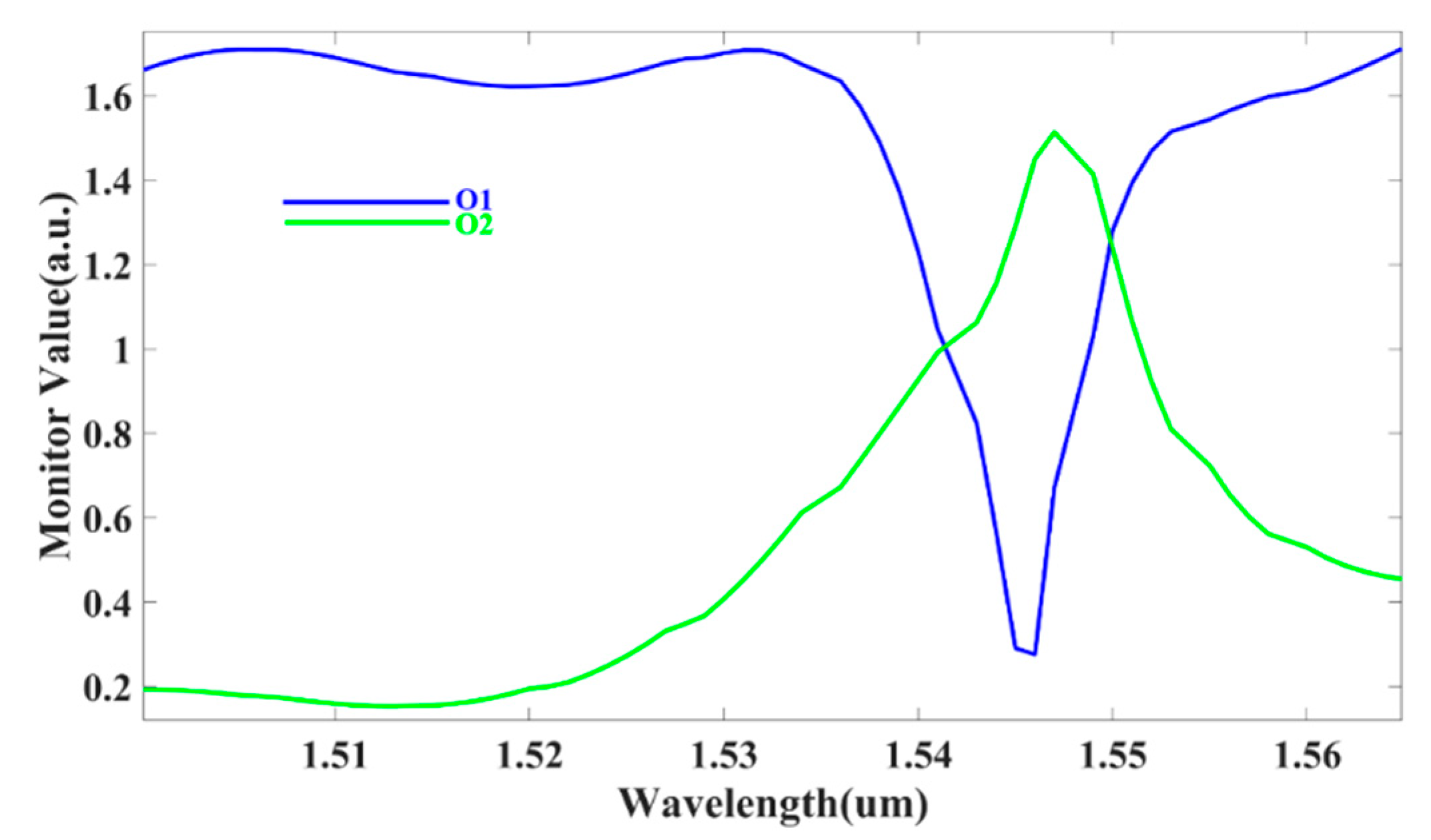
where c is the speed of light in vacuum, Δt is the time step, and Δx and Δz are mesh sizes in both X and Z directions. The second condition is about the grid spacing that should be less than λ/10. The time step was assumed Δt = 0.2 fs and the structure was discretized in which the length of unit cells was Δx = Δz = 100 nm. In the first stage, an optical pulse was applied to the input port and the pulse response was calculated at output ports. Figure 3 shows the frequency harmonic amplitude for O1 and O2 ports. It can be seen that the optical intensity between two output ports at λ = 1547 nm can be approached for switching applications.
To evaluate the resonance phenomenon, the transmission ratio for different input intensities was simulated (see in Figure 4). In this study, the intensity value at output port divides to input intensity is defined as the transmission ratio factor. When a signal is introduced to the input port, the output ports will be ON depending on the entrance optical intensity. If the input intensity is less than 0.235 W/µm2, the resonance wavelength of the ring will not change. As a result, O1 and O2 ports will be ON and OFF, respectively. The resonance wavelength can be changed because of the Kerr effect, so the optical waves will considerably be coupled to the O2 port for amounts of more than 0.235 W/µm2. In this case, O1 and O2 ports will be OFF and ON, respectively. It can be concluded that the threshold intensity for switching is around 0.235 W/µm2. This value is less than one in other works [45,57,59,60], so it can be considered an advantage of the proposed switch.
Figure 5 shows the normalized electric field distribution for two optical intensities, 0.1 W/µm2 and 0.45 W/µm2. A color bar has been inserted on the right side in which the red and black colors are the response in +1 and −1 for the domain amplitude of the field. It can be seen that optical waves are dropped from the upper waveguide to the lower waveguide for I = 0.45 W/µm2 while the dropping operation is not done for I = 0.1 W/µm2.
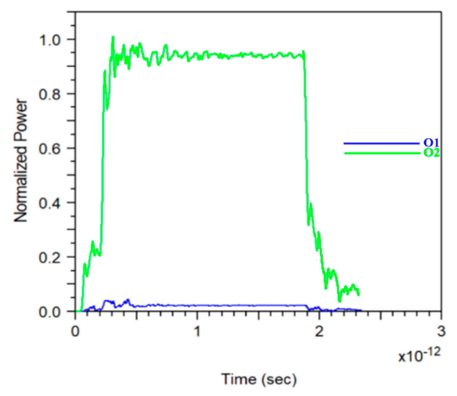
For more evaluation, the pulse response of the presented structure corresponding to Figure 5 has been calculated. As shown in Figure 6, the normalized powers at port O1 and O2 are obtained by 86% and 2% for I = 0.1 W/µm2, respectively, while ones are reached to 4% and 95% for I = 0.45 W/µm2. Also, as Figure 7 presents, the rise and fall times of the structure are obtained by 0.3 ps and 0.4 ps, respectively. The rise time is defined as the needed time for coupling the optical waves from one waveguide to another. This time is recorded when the power at the output port reaches 90% steady-state value. The fall time is assumed as the during time for decreasing power from a steady-state value to 10% of it. Comparing the obtained times with the ones in other works [75] demonstrates that the proposed graphene-based switch is faster than them. This characteristic is an essential factor in optical switching applications.
4. Discussion
Approaching the fast response of a switch is one of the main challenges for designing different switched-based applications. Furthermore, the small size of the structure results in it being capable of being considered for integrated circuits. Also, the low power and high contrast ratio are other important parameters for designing different switches. Some attempts have been done to improve the characteristics of optical switches [61,75].
In this study, a graphene-based all-optical switch has been presented in Section 2. Figure 5 and Figure 6 demonstrate the correct operation of the switch. To assess this work, the obtained results have been compared with references [57,58,59,60] in Table 1.
As presented in Figure 6, the time analysis shows that the proposed switch is faster than the one in other works [60]. Approaching the amount of 0.3 ps and 0.4 ps for rise and fall times is the main advantage of this work. Because of the large nonlinear coefficient of graphene in comparison with materials such as chalcogenide, silicon, nanocrystals, and gallium arsenide, the needed threshold intensity for switching operation in this study has been reduced to 0.235 W/µm2 in comparison to references [57,58,59,60]. This is another advantage of the graphene-based switch. Furthermore, the size of the proposed structure is less than the one in references [57,58,59,60]. It is obvious that the compactness of the switch is necessary for use in optical integrated circuits.
Contrast ratio of the output ports is calculated at 82%. The presented switch covers the high contrast ratio while this parameter has not been reported in references [57,58,59,60]. Besides all of these advantages, tuneability of some electrical and optical parameters for graphene is a principal characteristic for designing photonic crystal-based devices. Changing the refractive index of graphene in response to electric field affects optical power transmission toward the output ports. Also, the resonant frequency (or wavelength) of the switch could be changed to reach the desired value after the fabrication process.
5. Conclusions
In this study, a photonic crystal-based structure was proposed as an all-optical switch. Using the graphene-SiO2 stacks as rods in the resonant ring, switching operation was correctly approached. The rise and fall times of the device were obtained by 0.3 ps and 0.4 ps, respectively, that were less than the ones in other reports. The size of the presented structure was just about 70 µm2 and hence was smaller than the one in the aforementioned works of Section 1. The high nonlinear coefficient of the graphene resulted in a decreasing of the needed optical intensity to 0.235 W/µm2 for switching operation in comparison with other works. Furthermore, simulation results showed the contrast ratio of the switch was about 82%. In respect of the obtained results, it can be concluded that the presented all-optical switch is capable of consideration for optical integrated circuits.
Author Contributions
Formal analysis, M.R.J.A. and N.D.; Methodology, M.S. and M.R.J.A.; Writing-Original Draft, M.R.J.A.; Writing-Review and editing, M.S. and Y.S.-K.
Funding
This research received no external funding.
Conflicts of Interest
The authors declare no competing financial interest.
References
- Nagarajan, R.; Joyner, C.H.; Schneider, R.P.; Bostak, J.S.; Butrie, T.; Dentai, A.G.; Dominic, V.G.; Evans, P.W.; Kato, M.; Kauffman, M. Large-scale photonic integrated circuits. IEEE J. Sel. Top. Quantum 2005, 11, 50–65. [Google Scholar] [CrossRef]
- Bogaerts, W.; Chrostowski, L. Silicon photonics circuit design: Methods, tools and challenges. Laser Photonics Rev. 2018, 12, 1700237. [Google Scholar] [CrossRef]
- Yablonovitch, E. Inhibited spontaneous emission in solid-state physics and electronics. Phys. Rev. Lett. 1987, 58, 2059. [Google Scholar] [CrossRef] [PubMed]
- John, S. Strong localization of photons in certain disordered dielectric superlattices. Phys. Rev. Lett. 1987, 58, 2486. [Google Scholar] [CrossRef] [PubMed]
- Pu, S.; Dong, S.; Huang, J. Tunable slow light based on magnetic-fluid-infiltrated photonic crystal waveguides. J. Opt. 2014, 16, 045102. [Google Scholar] [CrossRef]
- Soljačić, M.; Johnson, S.G.; Fan, S.; Ibanescu, M.; Ippen, E.; Joannopoulos, J. Photonic-crystal slow-light enhancement of nonlinear phase sensitivity. JOSA B 2002, 19, 2052–2059. [Google Scholar] [CrossRef] [Green Version]
- Vlasov, Y.A.; O’boyle, M.; Hamann, H.F.; McNab, S.J. Active control of slow light on a chip with photonic crystal waveguides. Nature 2005, 438, 65. [Google Scholar] [CrossRef]
- Noori, M.; Soroosh, M.; Baghban, H. Highly efficient self-collimation based waveguide for Mid-IR applications. Photonics Nanostruct. 2016, 19, 1–11. [Google Scholar] [CrossRef]
- Noori, M.; Soroosh, M.; Baghban, H. All-angle self-collimation in two-dimensional square array photonic crystals based on index contrast tailoring. Opt. Eng. 2015, 54, 037111. [Google Scholar] [CrossRef]
- Witzens, J.; Loncar, M.; Scherer, A. Self-collimation in planar photonic crystals. IEEE J. Sel. Top. Quantum 2002, 8, 1246–1257. [Google Scholar] [CrossRef] [Green Version]
- Kosaka, H.; Kawashima, T.; Tomita, A.; Notomi, M.; Tamamura, T.; Sato, T.; Kawakami, S. Self-collimating phenomena in photonic crystals. Appl. Phys. Lett. 1999, 74, 1212–1214. [Google Scholar] [CrossRef]
- Rani, P.; Kalra, Y.; Sinha, R. Realization of AND gate in Y shaped photonic crystal waveguide. Opt. Commun. 2013, 298, 227–231. [Google Scholar] [CrossRef]
- Mansouri-Birjandi, M.A.; Tavousi, A.; Ghadrdan, M. Full-optical tunable add/drop filter based on nonlinear photonic crystal ring resonators. Photonics Nanostruct. 2016, 21, 44–51. [Google Scholar] [CrossRef]
- Tavousi, A.; Mansouri-Birjandi, M.A.; Ghadrdan, M.; Ranjbar-Torkamani, M. Application of photonic crystal ring resonator nonlinear response for full-optical tunable add–drop filtering. Photonic Netw. Commun. 2017, 34, 131–139. [Google Scholar] [CrossRef]
- Musavizadeh, S.M.; Soroosh, M.; Mehdizadeh, F. Optical filter based on photonic crystal. Indian J. Pure Appl. Phys. 2015, 53, 736–739. [Google Scholar]
- Qiang, Z.; Zhou, W.; Soref, R.A. Optical add-drop filters based on photonic crystal ring resonators. Opt. Express 2007, 15, 1823–1831. [Google Scholar] [CrossRef] [PubMed]
- Ying, C.; Jing, D.; Jia, S.; Qiguang, Z.; Weihong, B. Study on tunable filtering performance of compound defect photonic crystal with magnetic control. Optik 2015, 126, 5353–5356. [Google Scholar] [CrossRef]
- Dideban, A.; Habibiyan, H.; Ghafoorifard, H. Photonic crystal channel drop filter based on ring-shaped defects for DWDM systems. Phys. E 2017, 87, 77–83. [Google Scholar] [CrossRef]
- Mehdizadeh, F.; Soroosh, M. A new proposal for eight-channel optical demultiplexer based on photonic crystal resonant cavities. Photonic Netw. Commun. 2016, 31, 65–70. [Google Scholar] [CrossRef]
- Mehdizadeh, F.; Soroosh, M.; Alipour-Banaei, H. An optical demultiplexer based on photonic crystal ring resonators. Optik 2016, 127, 8706–8709. [Google Scholar] [CrossRef]
- Talebzadeh, R.; Soroosh, M.; Mehdizadeh, F. Improved low channel spacing high quality factor four-channel demultiplexer based on photonic crystal ring resonators. Opt. Appl. 2016, 46, 553–564. [Google Scholar]
- Talebzadeh, R.; Soroosh, M.; Kavian, Y.S.; Mehdizadeh, F. Eight-channel all-optical demultiplexer based on photonic crystal resonant cavities. Optik 2017, 140, 331–337. [Google Scholar] [CrossRef]
- Zavvari, M. Design of photonic crystal-based demultiplexer with high-quality factor for DWDM applications. J. Opt. Commun. 2019, 40, 135–138. [Google Scholar] [CrossRef]
- Khorshidahmad, A.; Kirk, A.G. Composite superprism photonic crystal demultiplexer: Analysis and design. Opt. Express 2010, 18, 20518–20528. [Google Scholar] [CrossRef] [PubMed]
- Jiu-Sheng, L.; Han, L.; Le, Z. Compact four-channel terahertz demultiplexer based on directional coupling photonic crystal. Opt. Commun. 2015, 350, 248–251. [Google Scholar] [CrossRef]
- Mehdizadeh, F.; Soroosh, M.; Alipour-Banaei, H. A novel proposal for optical decoder switch based on photonic crystal ring resonators. Opt. Quantum Electron. 2016, 48, 20. [Google Scholar] [CrossRef]
- Nozhat, N.; Taher Rahmati, A.; Granpayeh, N. An all optical switch based on nonlinear photonic crystal microcavities. In Proceedings of the Progress in Electromagnetics Research Symposium, Moscow, Russia, 18–21 August 2009. [Google Scholar]
- Serajmohammadi, S.; Alipour-Banaei, H.; Mehdizadeh, F. All optical decoder switch based on photonic crystal ring resonators. Opt. Quantum Electron. 2015, 47, 1109–1115. [Google Scholar] [CrossRef]
- Ouahab, I.; Naoum, R. A novel all optical 4 × 2 encoder switch based on photonic crystal ring resonators. Optik 2016, 127, 7835–7841. [Google Scholar] [CrossRef]
- Teo, H.; Liu, A.; Singh, J.; Yu, M.; Bourouina, T. Design and simulation of MEMS optical switch using photonic bandgap crystal. Microsyst. Technol. 2004, 10, 400–406. [Google Scholar] [CrossRef]
- Bai, J.; Wang, J.; Jiang, J.; Chen, X.; Li, H.; Qiu, Y.; Qiang, Z. Photonic not and nor gates based on a single compact photonic crystal ring resonator. Appl. Opt. 2009, 48, 6923–6927. [Google Scholar] [CrossRef]
- Hussein, H.M.; Ali, T.A.; Rafat, N.H. A review on the techniques for building all-optical photonic crystal logic gates. Opt. Laser Technol. 2018, 106, 385–397. [Google Scholar] [CrossRef]
- Saidani, N.; Belhadj, W.; AbdelMalek, F. Novel all-optical logic gates based photonic crystal waveguide using self-imaging phenomena. Opt. Quantum Electron. 2015, 47, 1829–1846. [Google Scholar] [CrossRef]
- haq Shaik, E.; Rangaswamy, N. Improved design of all-optical photonic crystal logic gates using T-shaped waveguide. Opt. Quantum Electron. 2016, 48, 33. [Google Scholar] [CrossRef]
- Andalib, P.; Granpayeh, N. All-optical ultracompact photonic crystal AND gate based on nonlinear ring resonators. J. Opt. Soc. Am. Rev. B 2009, 26, 10–16. [Google Scholar] [CrossRef]
- Fasihi, K. Design and simulation of linear logic gates in the two-dimensional square-lattice photonic crystals. Optik 2016, 127, 4669–4674. [Google Scholar] [CrossRef]
- Moniem, T.A. All-optical digital 4 × 2 encoder based on 2D photonic crystal ring resonators. J. Mod. Opt. 2016, 63, 735–741. [Google Scholar] [CrossRef]
- Hassangholizadeh-Kashtiban, M.; Sabbaghi-Nadooshan, R.; Alipour-Banaei, H. A novel all optical reversible 4 × 2 encoder based on photonic crystals. Optik 2015, 126, 2368–2372. [Google Scholar] [CrossRef]
- Haddadan, F.; Soroosh, M. Low-power all-optical 8-to-3 encoder using photonic crystal-based waveguides. Photon. Net. Comm. 2019, 37, 83–89. [Google Scholar] [CrossRef]
- Alipour-Banaei, H.; Rabati, M.G.; Abdollahzadeh-Badelbou, P.; Mehdizadeh, F. Application of self-collimated beams to realization of all optical photonic crystal encoder. Phys. E 2016, 75, 77–85. [Google Scholar] [CrossRef]
- Mehdizadeh, F.; Soroosh, M.; Alipour-Banaei, H. Proposal for 4-to-2 optical encoder based on photonic crystals. IET Optoelectron. 2016, 11, 29–35. [Google Scholar] [CrossRef]
- Rajasekar, R.; Latha, R.; Robinson, S. Ultra-contrast ratio optical encoder using photonic crystal waveguides. Matt. Lett. 2019, 251, 144–147. [Google Scholar] [CrossRef]
- Alipour-Banaei, H.; Ghorbanzadeh Rabati, M.; Abdollahzadeh-Badelbou, P.; Mehdizadeh, F. Effect of self-collimated beams on the operation of photonic crystal decoders. J. Electromagn. Wave 2016, 30, 1440–1448. [Google Scholar] [CrossRef]
- Mehdizadeh, F.; Alipour-Banaei, H.; Serajmohammadi, S. Study the role of non-linear resonant cavities in photonic crystal-based decoder switches. J. Mod. Opt. 2017, 64, 1233–1239. [Google Scholar] [CrossRef]
- Daghooghi, T.; Soroosh, M.; Ansari-Asl, K. A novel proposal for all-optical decoder based on photonic crystals. Photonic Netw. Commun. 2018, 34, 335–341. [Google Scholar] [CrossRef]
- Chattopadhyay, T.; Roy, J.N. An all-optical technique for a binary-to-quaternary encoder and a quaternary-to-binary decoder. J. Opt. A Pure Appl. Opt. 2009, 11, 075501. [Google Scholar] [CrossRef]
- Alipour-Banaei, H.; Mehdizadeh, F.; Serajmohammadi, S.; Hassangholizadeh-Kashtiban, M. A 2*4 all optical decoder switch based on photonic crystal ring resonators. J. Mod. Opt. 2015, 62, 430–434. [Google Scholar] [CrossRef]
- Zhang, C.; Qiu, K. Design and analysis of coherent OCDM en/decoder based on photonic crystal. Opt. Lasers Eng. 2008, 46, 582–589. [Google Scholar] [CrossRef]
- Tavousi, A.; Mansouri-Birjandi, M.A.; Saffari, M. Successive approximation-like 4-bit full-optical analog-to-digital converter based on Kerr-like nonlinear photonic crystal ring resonators. Phys. E 2016, 83, 101–106. [Google Scholar] [CrossRef]
- Mehdizadeh, F.; Soroosh, M.; Alipour-Banaei, H.; Farshidi, E. Ultra-fast analog-to-digital converter based on a nonlinear triplexer and an optical coder with a photonic crystal structure. Appl. Opt. 2017, 56, 1799–1806. [Google Scholar] [CrossRef]
- Mehdizadeh, F.; Soroosh, M.; Alipour-Banaei, H.; Farshidi, E. All optical 2-bit analog to digital converter using photonic crystal based cavities. Opt. Quantum Electron. 2017, 49, 38. [Google Scholar] [CrossRef]
- Mehdizadeh, F.; Soroosh, M.; Alipour-Banaei, H.; Farshidi, E. A novel proposal for all optical analog-to-digital converter based on photonic crystal structures. IEEE Photonics J. 2017, 9, 1–11. [Google Scholar] [CrossRef]
- Xu, C.; Liu, X. Photonic analog-to-digital converter using soliton self-frequency shift and interleaving spectral filters. Opt. Lett. 2003, 28, 986–988. [Google Scholar] [CrossRef] [PubMed]
- Youssefi, B.; Moravvej-Farshi, M.K.; Granpayeh, N. Two-bit all-optical analog-to-digital converter based on nonlinear Kerr effect in 2D photonic crystals. Opt. Commun. 2012, 285, 3228–3233. [Google Scholar] [CrossRef]
- Tajaldini, M.; Jafri, M.Z. An optimum multimode interference coupler as an all-optical switch based on nonlinear modal propagation analysis. Optik 2015, 126, 436–441. [Google Scholar] [CrossRef]
- Haché, A.; Bourgeois, M. Ultrafast all-optical switching in a silicon-based photonic crystal. Appl. Phys. Lett. 2000, 77, 4089–4091. [Google Scholar] [CrossRef]
- Alipour-Banaei, H.; Serajmohammadi, S.; Mehdizadeh, F. All optical NOR and NAND gate based on nonlinear photonic crystal ring resonators. Optik 2014, 125, 5701–5704. [Google Scholar] [CrossRef]
- Serajmohammadi, S.; Absalan, H. All optical NAND gate based on nonlinear photonic crystal ring resonator. IPA 2016, 3, 119–123. [Google Scholar] [Green Version]
- Alipour-Banaei, H.; Serajmohammadi, S.; Mehdizadeh, F. All optical NAND gate based on nonlinear photonic crystal ring resonators. Optik 2017, 130, 1214–1221. [Google Scholar] [CrossRef]
- Daghooghi, T.; Soroosh, M.; Ansari-Asl, K. A low power all optical decoder based on photonic crystal nonlinear ring resonators. Optik 2018, 174, 400–408. [Google Scholar] [CrossRef]
- Ogusu, K.; Yamasaki, J.; Maeda, S.; Kitao, M.; Minakata, M. Linear and nonlinear optical properties of Ag–As–Se chalcogenide glasses for all-optical switching. Opt. Lett. 2004, 29, 265–267. [Google Scholar] [CrossRef]
- Soh, D.B.S.; Hamerly, R.; Mabuchi, H. Comprehensive analysis of the optical Kerr coefficient of graphene. Phys. Rev. A 2016, 94, 023845. [Google Scholar] [CrossRef] [Green Version]
- Soavi, G.; Wang, G.; Rostami, H.; Purdie, D.G.; Fazio, D.D.; Ma, T.; Luo, B.; Wang, J.; Ott, A.K.; Yoon, D.; et al. Broadband, electrically tunable third-harmonic generation in graphene. Nat. Nanotechnol. 2018, 13, 583–588. [Google Scholar] [CrossRef] [PubMed] [Green Version]
- Jiang, T.; Huang, D.; Cheng, J.; Fan, X.; Zhang, Z.; Shan, Y.; Yi, Y.; Dai, Y.; Shi, L.; Liu, K.; et al. Gate-tunable third-order nonlinear optical response of massless Dirac fermions in graphene. Nat. Nanotechnol. 2018, 12, 430–436. [Google Scholar] [Green Version]
- Hendry, E.; Hale, P.J.; Moger, J.; Savchenko, A.K. Coherent Nonlinear Optical Response of Graphene. Phys. Rev. Lett. 2010, 105, 091401. [Google Scholar] [CrossRef] [PubMed]
- Virga, A.; Ferrante, C.; Batingnani, G.; Fazio, D.D.; Nunn, A.D.G.; Ferrari, A.C.; Cerullo, G.; Scopigno, T. Coherent anti-Stokes Raman Spectroscopy of single and multi-layer graphene. Nat. Commun. 2019, 10, 3658. [Google Scholar] [CrossRef] [PubMed]
- Khurgin, J.B. Graphene—A rather ordinary nonlinear optical material. Appl. Phys. Lett. 2014, 104, 16116. [Google Scholar] [CrossRef]
- Zhang, H.; Virally, S.; Bao, Q.; Ping, L.K.; Massar, S.; Godbout, N.; Kockaert, P. Z-scan measurement of the nonlinear refractive index of graphene. Opt. Lett. 2012, 37, 1856–1858. [Google Scholar] [CrossRef]
- Cheng, J.L.; Vermeulen, N.; Sipe, J.E. Third order optical nonlinearity of graphene. New J. Phys. 2014, 16, 053014. [Google Scholar] [CrossRef]
- Gu, T.; Petrone, N.; McMillian, J.F.; Zande, A.V.D.; Yu, M.; Lo, G.Q.; Kwong, D.L.; Hone, J.; Wong, C.W. Regenerative oscillation and four-wave mixing in graphene optoelectronics. Nat. Photonics 2012, 6, 554–559. [Google Scholar] [CrossRef] [Green Version]
- Johnson, S.G.; Joannopoulos, J.D. Block-iterative frequency-domain methods for Maxwell’s equations in a planewave basis. Opt. Express 2001, 8, 173–190. [Google Scholar] [CrossRef]
- Berman, O.L.; Boyko, V.S.; Kezerashvili, R.Y.; Kolesnikov, A.A.; Lozovik, Y.E. Graphene-based photonic crystal. Phys. Lett. A 2010, 374, 4784–4786. [Google Scholar] [CrossRef] [Green Version]
- Saleh, B.E.A.; Teich, M.C. Fundamentals of Photonics; John Wiley & Sons: Hoboken, NJ, USA, 1991; Chapter 19. [Google Scholar]
- Sullivan, D.M. Electromagnetic Simulation Using the FDTD Method; John Wiley & Sons: Hoboken, NJ, USA, 2013. [Google Scholar]
- Daghooghi, T.; Soroosh, M.; Ansari-Asl, K. Ultra-fast all-optical decoder based on nonlinear photonic crystal ring resonators. Appl. Opt. 2018, 57, 2250–2257. [Google Scholar] [CrossRef] [PubMed]
Figure 1.
The band diagram of the proposed structure.
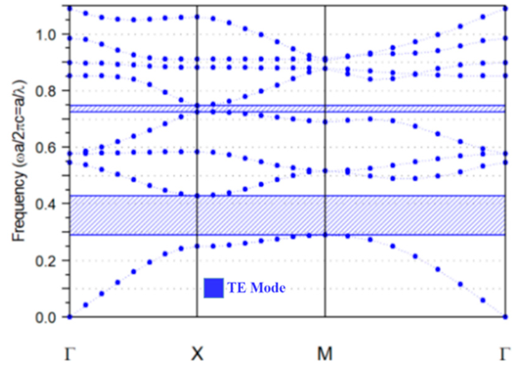
Figure 2.
The proposed all-optical switch.
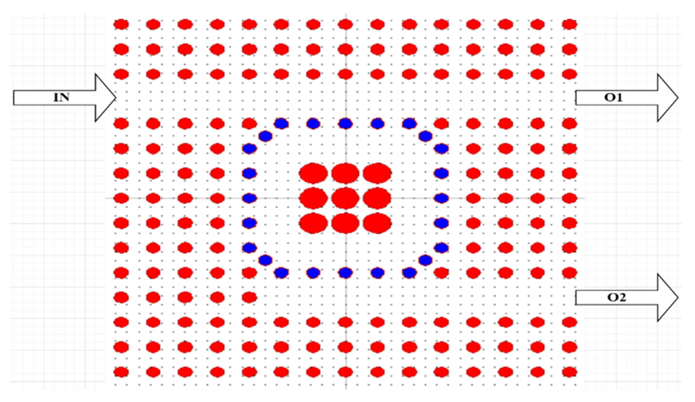
Figure 3.
Response of the switch for different wavelengths.

Figure 4.
Transmission ratio of the structure for different input intensities.
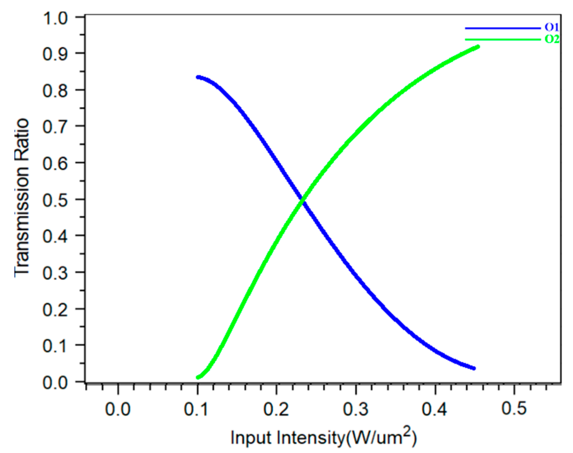
Figure 5.
Electric field distribution into the structure for: (a) I = 0.45 W/µm2; (b) I = 0.1 W/µm2.
Figure 5.
Electric field distribution into the structure for: (a) I = 0.45 W/µm2; (b) I = 0.1 W/µm2.
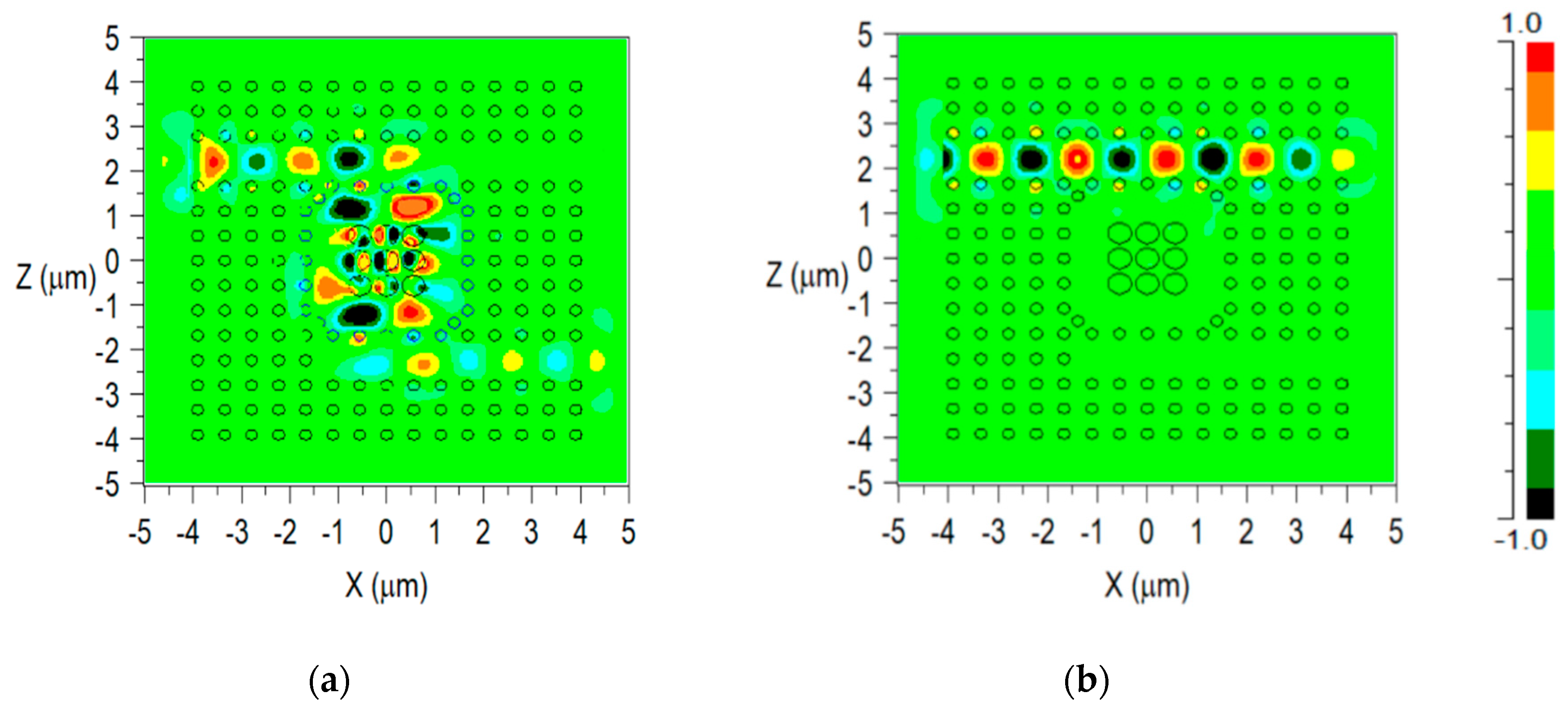
Figure 6.
The normalized output power for: (a) I = 0.45 W/µm2; (b) I = 0.1 W/µm2.
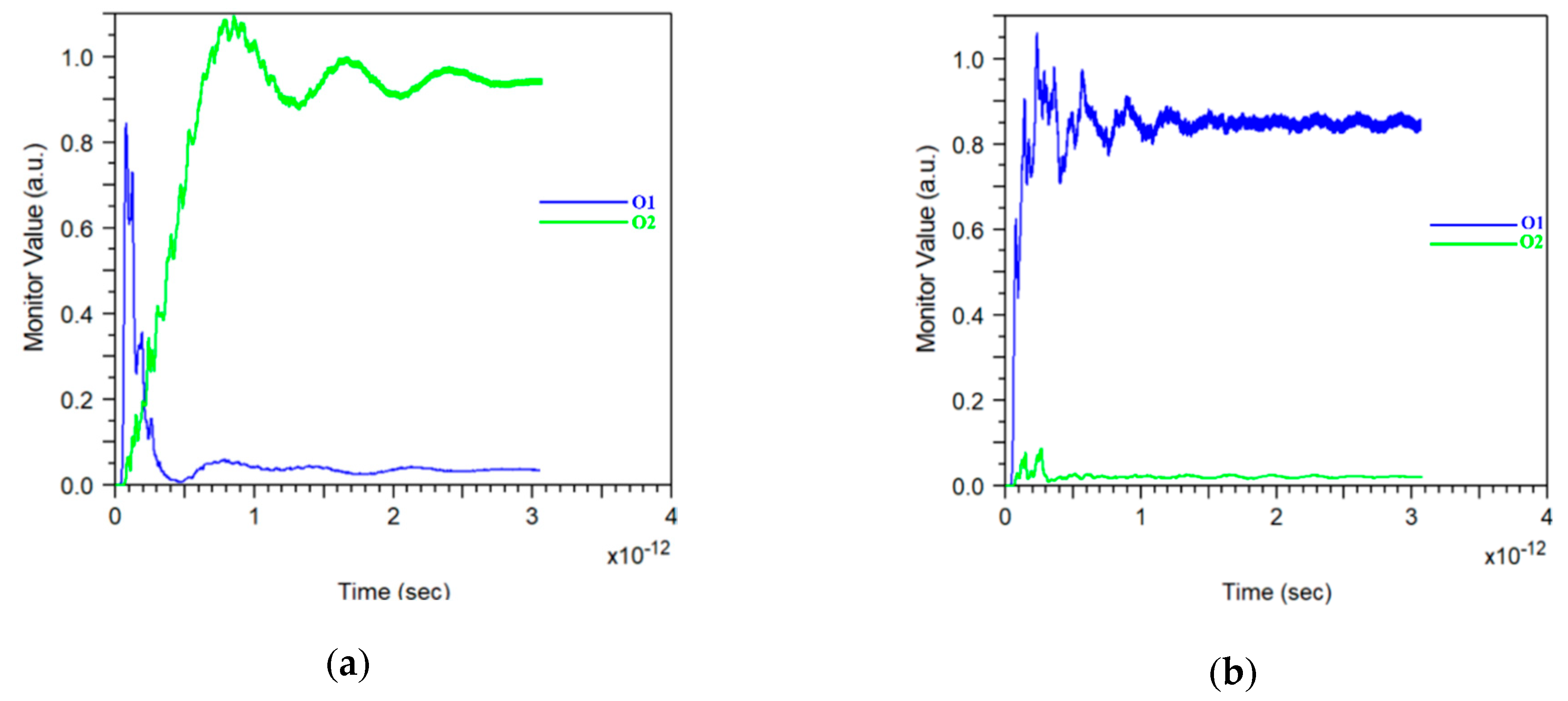
Figure 7.
The pulse response for proposed optical switch.

© 2019 by the authors. Licensee MDPI, Basel, Switzerland. This article is an open access article distributed under the terms and conditions of the Creative Commons Attribution (CC BY) license (http://creativecommons.org/licenses/by/4.0/).
Share and Cite
MDPI and ACS Style
Jalali Azizpour, M.R.; Soroosh, M.; Dalvand, N.; Seifi-Kavian, Y. All-Optical Ultra-Fast Graphene-Photonic Crystal Switch. Crystals 2019, 9, 461. https://doi.org/10.3390/cryst9090461
AMA Style
Jalali Azizpour MR, Soroosh M, Dalvand N, Seifi-Kavian Y. All-Optical Ultra-Fast Graphene-Photonic Crystal Switch. Crystals. 2019; 9(9):461. https://doi.org/10.3390/cryst9090461
Chicago/Turabian StyleJalali Azizpour, Mohammad Reza, Mohammad Soroosh, Narges Dalvand, and Yousef Seifi-Kavian. 2019. "All-Optical Ultra-Fast Graphene-Photonic Crystal Switch" Crystals 9, no. 9: 461. https://doi.org/10.3390/cryst9090461
Note that from the first issue of 2016, this journal uses article numbers instead of page numbers. See further details here.