1. Introduction
Photonic crystal (PC), an artificial material in which the refractive index is modulated at wavelength scale, offers presently many interesting applications in different domains [
1,
2]. The most important property of the PCs is the existence of a so-called photonic bandgap (PBG). In case of one-dimensional (1D) PCs, the PBG can be easily obtained by assembling multiple layers of two different materials with very low refractive indices contrast [
3,
4,
5,
6]. However, in case of two- and three-dimensional (2D and 3D) PCs, it requires that the refractive indices contrast should be as high as possible. Some 2D and 3D PCs are made by polystyrenes or SiO
nanoparticles [
7,
8,
9,
10], which are fabricated by a simple fabrication method, but these PCs do not have a true PBG, or in other word, they have a so-called pseudo or partial PBG, due to their weak refractive index. Therefore, most 2D and 3D PCs are made by semiconductor materials with high refractive indices, which however makes the fabrication procedure complicated and expensive. Different optimizations have been proposed to obtain the PBG as large as possible and with a material with a smaller refractive index. By increasing the symmetry of the PCs, for example in the case of 2D PCs, from square (four-fold) to hexagon (six-fold), and to quasi-periodic PCs, such as Penrose structure [
11,
12], the PBG can be opened at lower refractive index materials, such as polymers [
13,
14].
The most difficult task of PCs investigations is the fabrication, which should satisfy several conditions, such as simple, rapid, inexpensive, and particularly flexible. Today, many fabrication techniques have been proposed to realize PCs, for example, e-beam lithography, self-assembly of opals, laser interference, and direct laser writing. The choice of fabrication technique depends on desired applications. Among available fabrication technologies, the direct laser writing (DLW) is the most powerful one allowing fabrication of any desired PCs, in multi-dimension ((1D, 2D, 3D) PCs) [
15,
16]. The working principle of the DLW is to focus tightly a laser beam into a small region of a photoresist to induce a local polymerization or depolymerization effect. By moving the focusing spot following a well-designed structure, a corresponding polymeric pattern can be obtained.
In this work, we demonstrated an optimization of the 2D PCs to obtain a large PBG even with low refractive index materials, such as polymer. We proposed an original idea of high symmetry 2D PCs, and a new experimental way to realize these PCs by the DLW technique. The PBGs of a standard honeycomb structure and of a newly proposed structure are calculated and compared by using a Finite-difference time-domain (FDTD) method. These structures are then fabricated by a new scanning method using the one-photon absorption-based DLW technique [
17].
2. Theoretical Calculation
For calculation of the PBG of different PCs, we have used the FDTD method (Lumerical Software) with Bloch boundary conditions. We assumed that the refractive index of material is 1.6, a typical value of polymer without considering the dispersion effect of the material. This choice is justified by the values experimentally measured in our case, i.e.; the refractive index of the used polymer is in between 1.55 and 1.62 for the wavelengths ranging from 400 nm to 800 nm. For simulations of 2D PCs, we distinguished two different modes, TM and TE, which are the transverse magnetic or transverse electric modes where the magnetic or electric field is parallel to the PC plane, respectively.
It is well-known that the honeycomb lattice is the best 2D PC, which provides a largest PBG, as compared to the square or hexagonal lattice. We first calculated the PBG of this structure at low refractive index material, by considering two types: one is the honeycomb lattice comprising of polymeric cylinders (
n = 1.6) in an air background (
n = 1) and the another is an inverse geometry consisting of air-holes in the polymeric background.
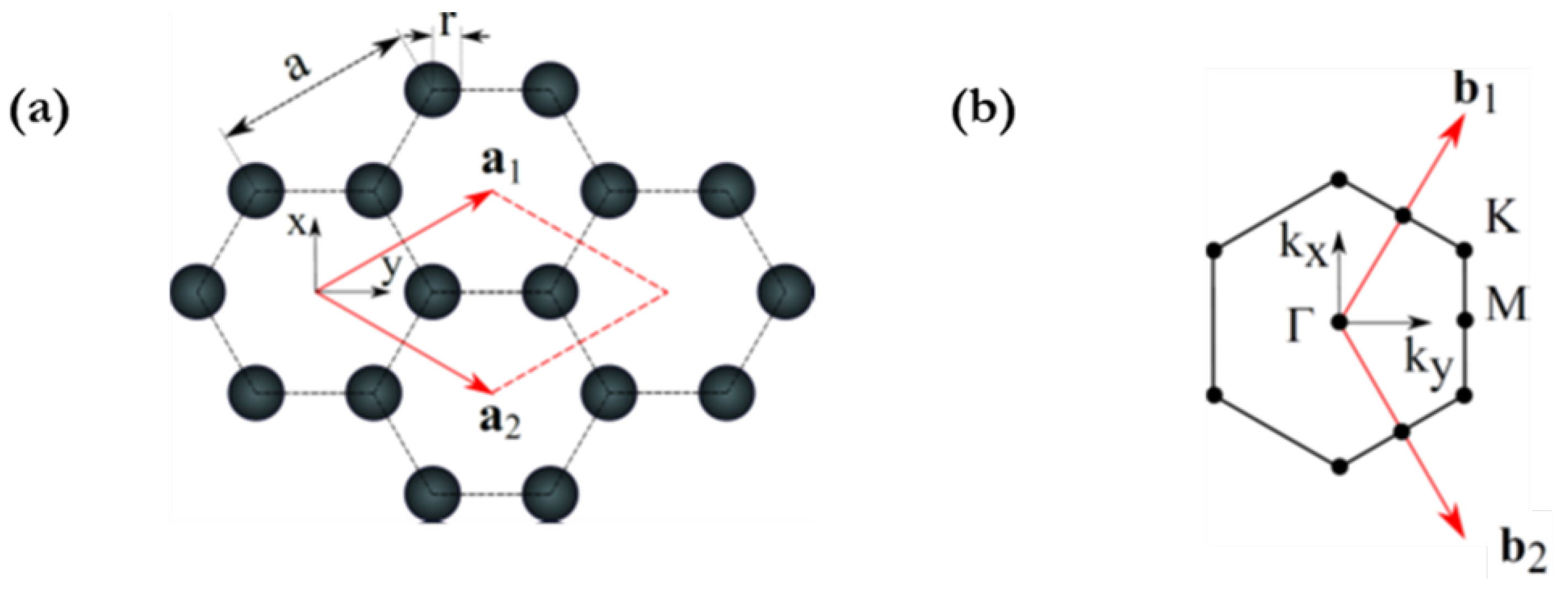
Figure 1a,b show a honeycomb lattice and its reciprocal space, where a is lattice constant, and r is the radius of polymeric cylinders or air-holes. For the case of polymeric cylinders in the air background, the PBG only reveals a small gap for TE mode.
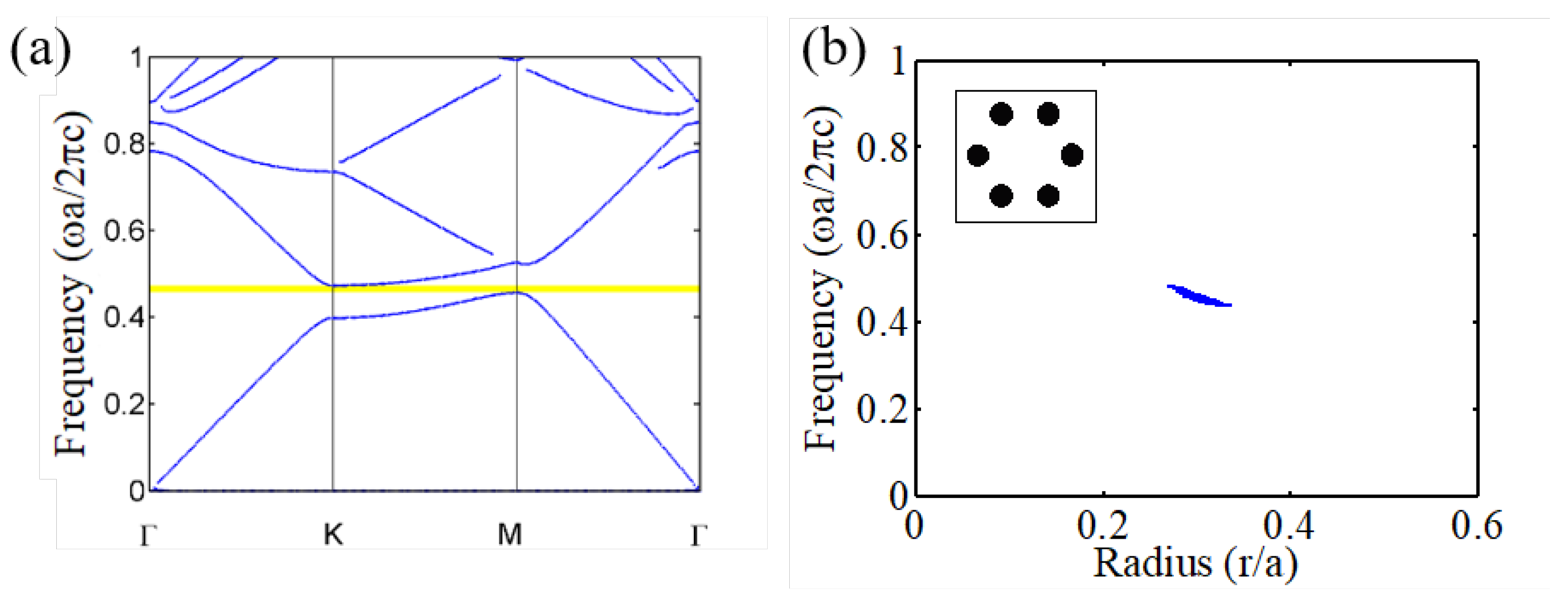
Figure 2a shows a band structure for TE mode, obtained with an optimum radius of r/a = 0.3.
Figure 2b shows gap map obtained with various filling factors (different ratios of r/a). We see that the largest PBG for TE mode is about 0.02 at r = 0.3a. When considering a honeycomb lattice made of air cylinders in the polymeric background, we found that the PBG only reveals for TM mode. A band structure for TM mode (r/a = 0.35) is shown in
Figure 3a. The PBG (for TM mode) as a function of the r/a ratio was also calculated, and a gap map is presented in the
Figure 3b. We can see that the PBG is increased as compared to the one obtained in previous case, and reaches 0.05 at r = 0.35a. These results are somehow similar to results obtained with higher refractive index [
1,
2]. But at low refractive index material, the PBG exists but not complete, i.e.; no common PBG for both TE and TM modes.
Table 1 summarizes the PBG of the honeycomb lattice at low refractive index material for both configurations.
It has been well-known that the larger PBG can be obtained by increasing the structure symmetry [
18]. Different structures have been proposed [
11,
12,
13,
14], and larger PBG are obtained, even at low refractive index materials. In particular, it is important to emphasis on the most symmetric one, called circular photonic crystal (CPC) [
19,
20], which possesses a perfect symmetry in a 2D plane. This CPC structure enables particularly an isotropic PBG, and consequently a PBG at low refractive index. However, the CPC is a non-periodic structure and usually developed around a symmetric point. Therefore, its photonic property is only characterized by a transmission calculation or measurement but not its PBG.
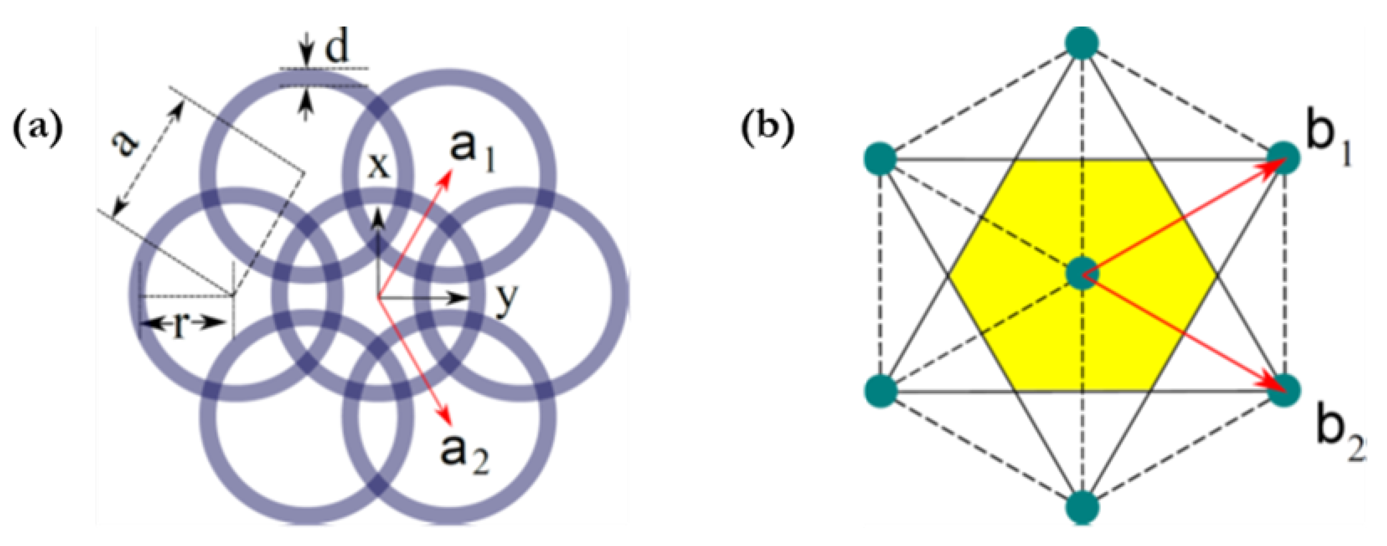
In this work, we proposed a novel kind of equivalent 2D PC by arranging multi-rings in a periodic configuration, such as a hexagonal lattice. This novel structure allowed us to combine the advantages of both CPC structure, thanks to the perfect symmetry of the rings (dielectric or air), and the periodic organization of these rings in a well-known hexagonal lattice, which can be numerically simulated to obtain a true PBG. As it will be shown in the experimental part, the proposed structure is also matched to the capacity of the fabrication technology.
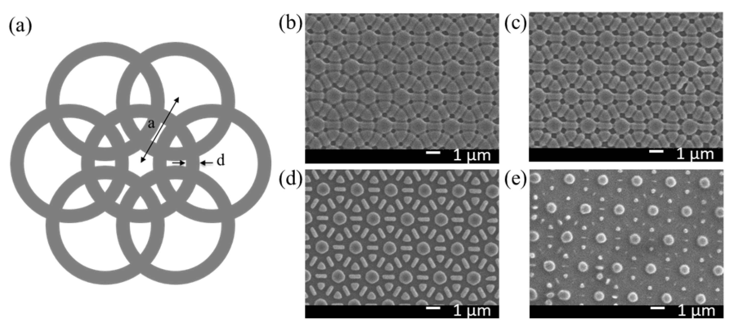
Figure 4a presents an assembled multi-rings lattice and
Figure 4b illustrates its corresponding reciprocal space, where a is the lattice constant, r is the radius of the rings, and d is the width of rings. Similar to honeycomb PC, the PBG of the assembled multi-rings lattice can be calculated for two possible configurations: the lattice containing multi-rings of air (
) in the polymeric background (
) and the another is an inverse geometry consisting of multi-rings of polymer in the air background. In practices, these two configurations can be optically realized by using a negative photoresist or a positive photoresist, or simply by using a positive photoresist with controllable laser power [
17]. We demonstrated that the multi-rings assembly allowed obtaining different 2D PCs with various filling factors. That can be done by changing the r/a ratio. It is clear that if a > 2r, all rings will be separated, and the structure is a simple hexagonal PC with a ring as an “artificial atom”. However, if a < 2r, multiple rings will overlap to each other, resulting in a complicated 2D PC, with a perfect symmetry determined by the ring.
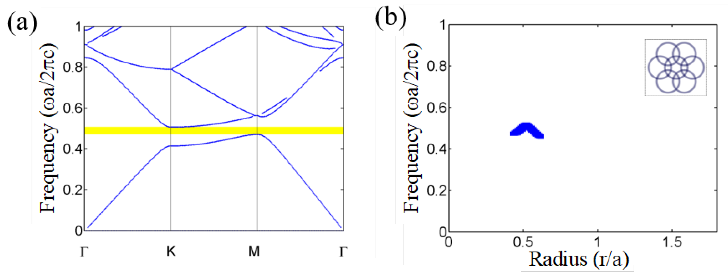
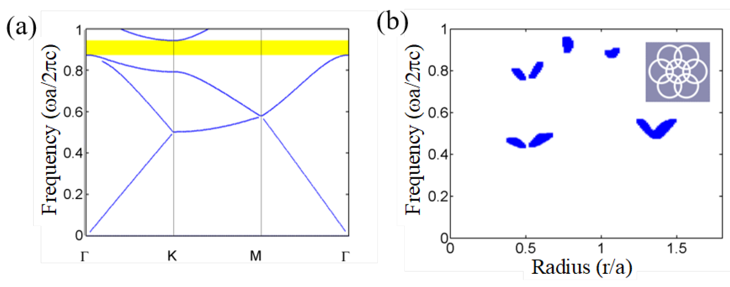
Figure 5 shows the simulation results for the case of assembled polymeric multi-rings (
) in the air background. Similar to the case of the honeycomb, it has seen that the PBG reveals only for TE mode. For the simulation shown in
Figure 5a, we assumed that the ring width is 300 nm, the ring separation a = 1.5
m, and the ring radius r/a = 0.51, which is suitable to the fabrication capacity. A larger PBG is obtained, as compared to similar case of the honeycomb lattice shown in
Figure 2a. By changing the radius of rings, a gap map (shaded blue region) as a function of r/a for TE mode has been carried out, and shown in
Figure 5b. It can be seen that the largest PBG is obtained with a value of a
/2
c = 0.035 with r = 0.51a.
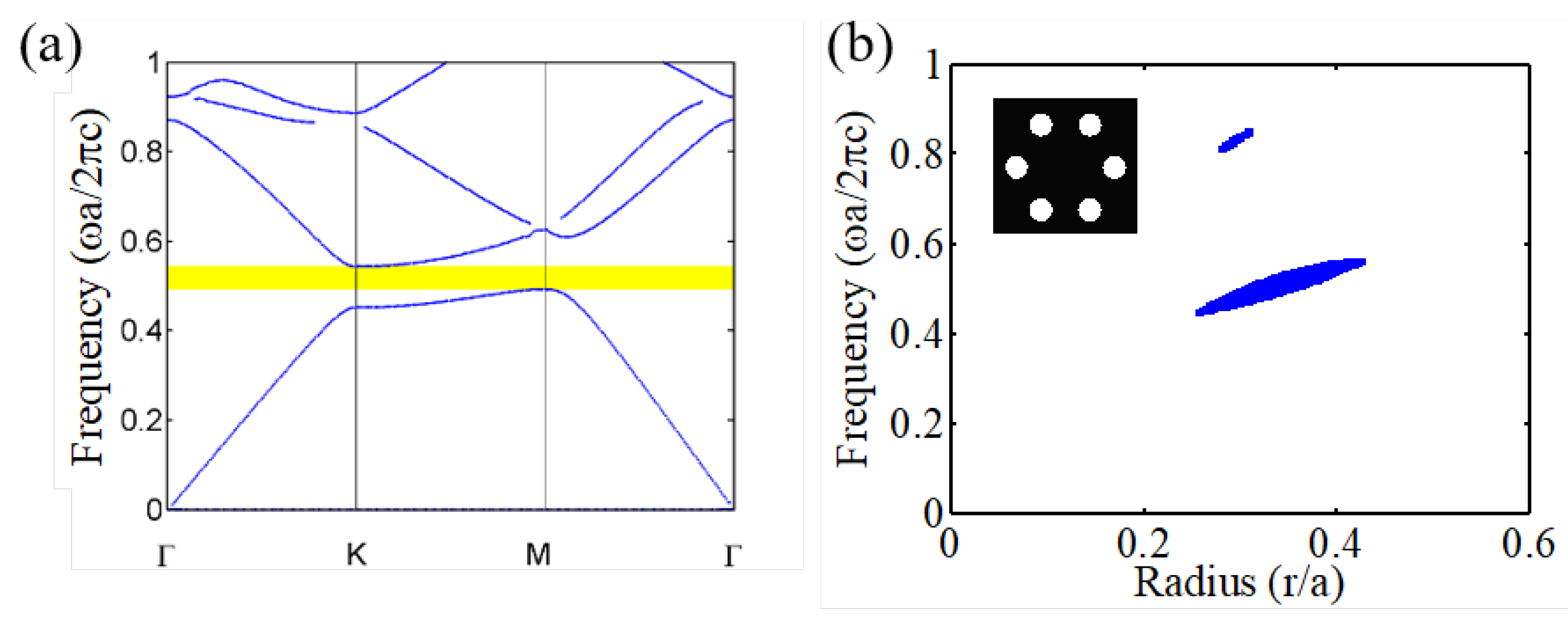
For the case of a 2D lattice consisting of air rings (
n = 1) in the polymeric background, in contrast, the PBG reveals only for TM mode.
Figure 6a shows its PBG obtained with a radius ratio of r/a = 0.78 with a = 1.5
m. Again, the PBG is larger, as compared to that obtained by the honeycomb lattice shown in
Figure 3a. A map of PBGs for TM mode versus the ratio of r/a is shown in
Figure 6b. It can be seen that multiple gaps can be obtained with this structure, even with low refractive index contrast. The PBG can reach a value of a
/2
c = 0.089 at r = 0.78a, which is larger than 0.05, obtained by the honeycomb PC. A summary of PBGs of multi-rings lattice is shown in
Table 2. This novel PC still does not produce a complete PBG, but the individual PBG (for TE or TM mode) is better than those obtained by a best standard 2D PC (e.g., honeycomb).
We note that in a standard case of square or hexagonal 2D PCs, the rod-type has a TM-bandgap and the hole-type has a TE-bandgap, respectively [
1,
2]. However, when working with particular structures, such as honeycomb or multi-ring PCs, the situation changes. In these cases, the existence of TM or TE bandgaps varies as a function of the ratio between the rod size and the lattice periodicity. With low refractive index, we can see that the rod-type favors a TE-bandgap while the hole-type favors a TM-bandgap, respectively.
3. Fabrication of Proposed Structure by Direct Laser Writing Method
To fabricate these proposed PCs, two possible methods can be used, such as e-beam lithography and DLW method. In this work, we have demonstrated the fabrication by using one-photon absorption-based DLW method, which is simple, low cost, and it can even produce 3D PCs [
16,
17,
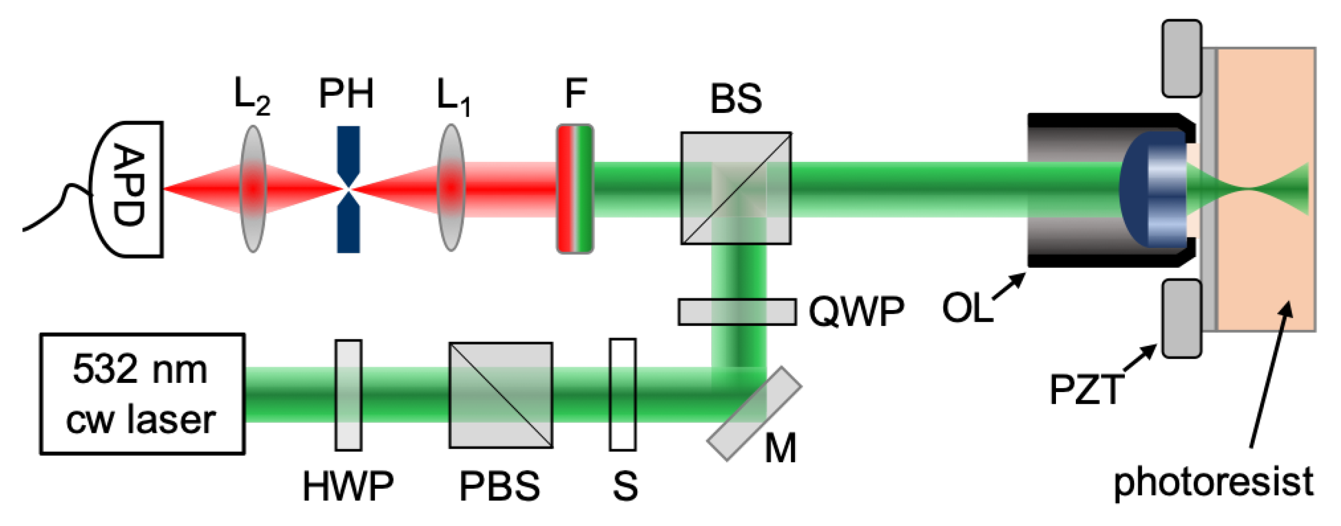
21]. The experimental setup is shown in
Figure 7 and can be explained as follows. A simple and low-cost continuous-wave (cw) 532 nm laser was used to write the desired structures. The laser power was adjusted by using a combination of a half-wave plate and a polarizing beam splitter. The laser beam is sent through an electronic shutter (S), which allows controlling the exposure time. The quarter-wave plate was used to obtain a circular polarization of the excitation beam, just before focusing. The laser beam was sent on a 50/50 beam-splitting cube (BS), after which one part goes to a powermeter and the other is directed to an oil-immersion objective lens (OL) with a numerical aperture (NA) of 1.3, which focuses the laser beam on the photoresist sample. The last one was placed on a piezoelectric translation stage (PZT), which allows moving the sample in 3D with a resolution of 0.1 nm. Thanks to the high NA OL, the laser is tightly focused onto the sample with a focusing spot of about 300 nm. To determine the focusing position, the same OL is used to collect the fluorescence photons, emitted from the photoresist sample, which then propagate in opposite direction with respect to the excitation beam. The fluorescence beam is passed through a long-pass filter (F) with a cut-off wavelength of 580 nm, to remove the excitation laser light, and directed towards an avalanche photodiode (APD). It has been demonstrated that this technique can fabricate structures with a thickness as large as 100 micrometers, depending on the absorption coefficient of the photoresist [
16,
21], with a periodicity down to 400 nm and the smallest size of pattern can be as small as 57 nm [
17].
In this work, we proposed a new way to realize desired structures. Indeed, in e-beam lithography or DLW, the structures are usually created by moving the focusing spot following a design. We proposed to assembly multiple lines or rings to achieve desired structures. Various structures can be created with the same lines or rings assembly, which simplifies a lot for fabrication procedure. For demonstration, we used a positive S1818 photoresist with a thickness of
m. With low excitation laser power, the focusing spot produced an air-hole in polymer thin film (after development), and by moving this focusing, we obtained an assembly of air multi-rings lattice. Please note that with the same photoresist and with higher excitation laser power, we can obtain a polymeric multi-ring thanks to the optically induced thermal effect [
17].
Figure 8a shows a new proposed trajectory of the focusing laser beam to draw a honeycomb lattice. By this method, we can obtain different structures, starting from a standard air-hole hexagonal structure to a honeycomb structure with controllable filling factors and dots shape.
Figure 8b–e show scanning electron microscope (SEM) images of different structures (period of a = 1.5
m) fabricated by a constant laser power of
W and by different moving velocities from
m/s to
m/s. We can see that with velocities of
m/s and
m/s, typical hexagons with air-holes are obtained, while with velocities of
m/s and
m/s (higher dose), honeycombs with different filling factors are demonstrated. Thus, by using the simple scanning scheme shown in
Figure 8a, and by controlling the scanning speed, various types of honeycomb lattices can be obtained.
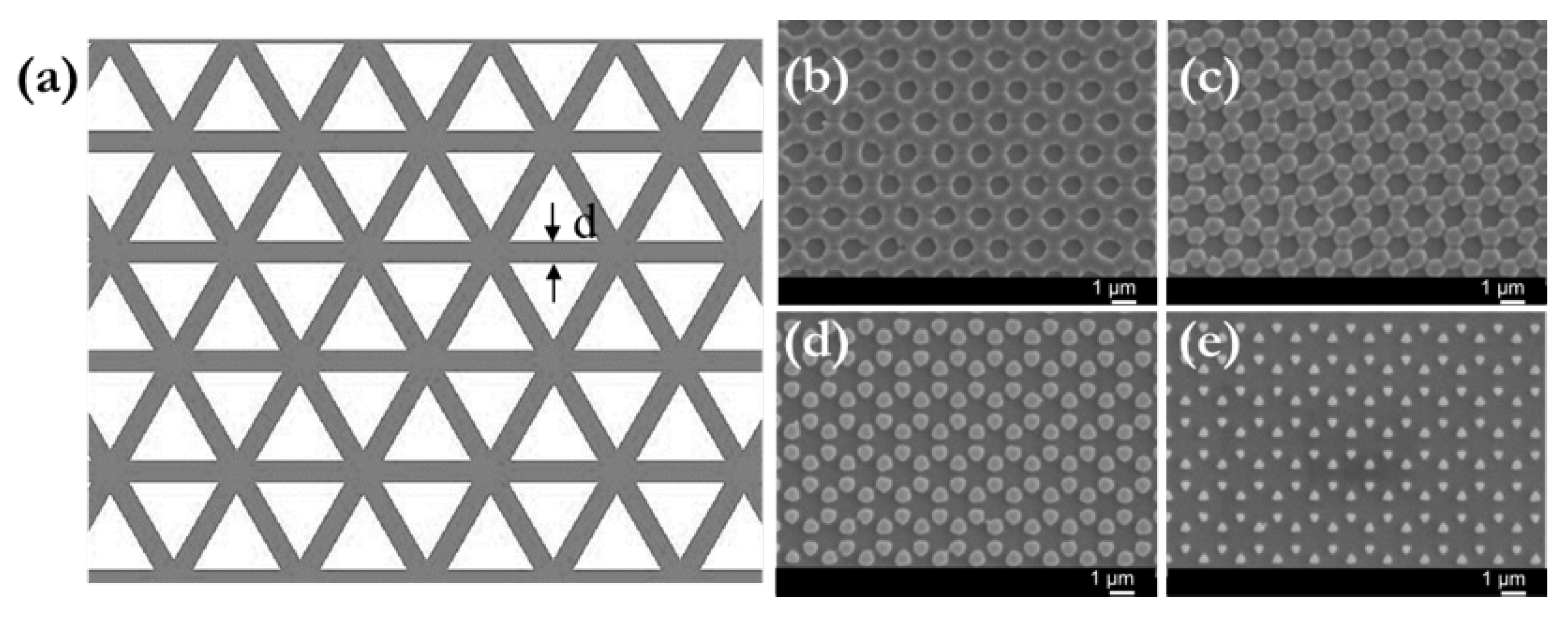
By the same method, assembled multi-rings lattices were fabricated by scanning the focusing laser beam following the trajectory shown in
Figure 9a. Different structures have been demonstrated by changing the structures parameters, such as the ring width, d, the lattice constant, a, as well as the ring radius, r.
Figure 9b–e show SEM images of four structures realized by keeping the same laser power,
W while changing the moving velocities of laser beam from
m/s to
m/s. The lattice constant and the ring radius were chosen as 2
m and 1.51
m, respectively. When varying the scanning velocities, the ring width changes from 150 nm (
Figure 9b), 200 nm (
Figure 9c), 300 nm (
Figure 9d), to 400 nm (
Figure 9e), resulting in different 2D structures with different filling factors and structure compositions. This perfectly agrees with the theoretical prediction, and their PBGs are also demonstrated to be better than those obtained by the standard 2D PCs.
Please note that it is not possible at this moment to experimentally characterize the PBGs of these fabricated structures, because the structures sizes are limited to m × 100 m due to the scanning system of the DLW technique. Also, with a lattice constant of 2m, an assembled multi-rings PC produces a PBG in the range of 2.85–3.15 m, which is in the mid-infrared domain. The limited PC thickness (1m) also makes the direct PBG characterization difficult. Further reduction of the lattice constant (a) and of the ring radius (r), and increase of the PCs thickness are therefore necessary to obtain a PBG in visible or near IR range, which can be very promising for many applications. A direct application of such fabricated structures is to make PC-based organic laser, with controllable emission wavelength and desired beam shape.


