Article

Liquid-Phase Epitaxial Growth and Characterization of Nd:YAl3(BO3)4 Optical Waveguides

MQ Photonics, Department of Physics and Astronomy, Macquarie University, 2109 Sydney, Australia
*
Author to whom correspondence should be addressed.
Crystals 2019, 9(2), 79; https://doi.org/10.3390/cryst9020079
Submission received: 16 December 2018 / Revised: 25 January 2019 / Accepted: 28 January 2019 / Published: 1 February 2019
(This article belongs to the Special Issue Crystal Growth of Multifunctional Borates and Related Materials)

Abstract

:
We investigated the fabrication of neodymium doped thin film optical waveguide-based devices as potential active sources for planar integrated optics. Liquid-phase epitaxial growth was used to fabricate neodymium-doped yttrium aluminum borate films on compatible lattice-matched, un-doped yttrium aluminum borate substrates. We observed the refractive index contrast of the doped and un-doped crystal layers via differential interference contrast microscopy. In addition, characterization by X-ray powder diffraction, optical absorption and luminescence spectra demonstrated the crystal quality, uniformity and optical guiding of the resulting thin films.

Graphical Abstract

1. Introduction

Integrated optics and photonics are increasingly important for optical signal processing in many applications. They rely on the development of compact, robust planar optical devices. Integrated optics employ waveguides as the building blocks for optical components, which are then connected into circuits [1]. In particular, integrated optical systems using waveguide-based components typically include active devices such as lasers and modulators that are integrated into photonic circuits. In each case, the structure must be designed to guide and confine the light within the active region of the device via the careful design of the refractive index contrast between the cladding and the active layer. Optical waveguides are described as single mode or multimode, based on the properties of the structure, as determined by the refractive index and dimensions of the guiding layer and substrate or cladding [2]. Active waveguide devices offer particular advantages over their bulk counterparts, because the optical confinement increases the intensity of the signal and pump light within the waveguide, hence ensuring that the amplification or nonlinear optical frequency conversion is more efficient than comparable bulk devices [3]. Here, we consider multimode active planar dielectric devices.
Fabrication of planar waveguide devices has been accomplished by a variety of approaches [3]. For example, the refractive index inside a dielectric material may be modified using nonlinear multiphoton processes [4,5], or ion-exchange [6]. In another approach, two crystals may be optically polished and then thermally bonded to achieve strong adhesion between the crystal layers [7]. This typically requires careful polishing to ensure that the active layer is sufficiently flat and thin. Epitaxial growth processes [8], such as liquid phase epitaxy (LPE) [9], pulsed laser deposition [10], molecular beam epitaxy (MBE) [11], hydrothermal epitaxy [12], metal oxide chemical vapor deposition (MOCVD) [13], and halide vapor phase epitaxy (HVPE) [14], enable the production of high-quality crystalline materials, which are practical for waveguide fabrication.
There has been long-standing interest in multifunctional-doped borate laser crystals [15,16,17,18,19,20,21,22,23,24], which are used in compact robust lasers emitting fundamental or self-frequency-doubled wavelengths, with Q-switched, mode-locked or continuous wave operation. The thermal conductivity of these crystals facilitates the operation of the lasers at high power and in thin disk geometries [25,26,27]. In addition, un-doped borates have been adopted for nonlinear optics [28,29]. This has led to a new drive for improved growth techniques for these crystals. Various approaches to optimize the crystal growth—the choice, preparation, mixing of the flux, and the temperature profile—have been reported [15,16,17]. There is a balance between the relatively slow growth of the crystals, and the control of the crystal phase and uniformity, due to the formation of crystal twins [30,31]. However, following an early report of epitaxial film growth [32], there has been recent interest in developing borate crystals for waveguide devices that are compatible with integrated optics. This geometry enables the concentration of the light in the active layer to enhance both the amplification and the optical nonlinearity of the device [33,34,35,36].
The liquid phase epitaxial growth technique has several advantages compared with other waveguide fabrication techniques. The layers are grown isothermally with homogeneous composition, so the quality of the epitaxial layer is comparable with that of bulk materials. The interface between the thin film and the substrate exhibits a step profile in the refractive index, whereas other waveguide fabrication techniques typically lead to graded index profiles. Generally, the modes propagating inside a multimode step index profile structure have a uniform effective index, whereas for a graded index profile, different modes have a different effective index. The thickness of the waveguide structure can be controlled accurately by the growth duration and growth temperature. Finally, liquid phase epitaxy is adaptable for any single crystalline layer or active dopant, using an appropriate flux system and growth conditions [8].
We investigated liquid phase epitaxy as an effective growth method for Nd:YAl3(BO3)4 (Nd:YAB) thin films on compatible lattice-matched un-doped borate substrates. The resulting films, whose lattice constants are consistent with R32 crystal symmetry, exhibit very good optical properties. Differential interference contrast microscopy, X-ray powder diffraction and optical absorption and luminescence spectra were used to characterize the optical quality and uniformity of these thin films.

2. Crystal Growth

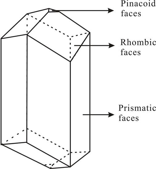
2.1. Crystal Growth Methods

The flux system for the Nd:YAB epitaxial growth was chosen to be K2Mo3O10 with excess Y2O3 and B2O3 [16]. This flux system offers advantages, because it has lower volatility than the PbF2-3B2O3 flux system, and excess Y2O3 and B2O3 were added to the initial flux to suppress Al5BO9 inclusions and to compensate for the volatility of B2O3 during crystal growth [16]. The mix for the growth was calculated as 8 at. % Nd/(Nd + Y) with 24.4 wt. % of Nd:YAB in the solution. The solvent composition was 91.9 wt. % of K2Mo3O10 + 5.4 wt. % B2O3 + 0.25 wt. % Y2O3. All the chemicals were obtained from local suppliers and heat-treated in a 300 °C furnace to remove adsorbed water before weighing. They were completely ground and mixed in the platinum crucible (5 cm diameter) and heated in an electric resistance furnace at 1150 °C for 24 h. The temperature was then dropped to about 1000 °C to find the actual saturation point by repeated seeding. The seed was settled to the mid part of the solution to ensure a homogeneous temperature gradient.
The substrate for the thin film growth needs to be selected carefully. It must permit reasonable lattice matching with the epitaxial layer to avoid strain due to lattice mismatch, and it must ensure a refractive index contrast, so that the active layer is the guiding layer with a higher refractive index. We selected un-doped YAl3(BO3)4 (YAB), as it satisfies these criteria well. We also determined that a neodymium fraction of 8% permitted waveguide confinement, without excessive lattice mismatch. The calculated refractive index contrast for 8 at % Nd dopant is 0.0632 for no and 0.0608 for ne [16]. Figure 1a shows the prismatic faces {11 2 ¯ 0} and {2 1 ¯ 1 ¯ 0} and the rhombic face {01 1 ¯ 1} for Nd:YAB, along with the crystal axes in Figure 1b. Previous liquid phase epitaxial growth of NdAB yielded thin films of good quality using Gd0.59La0.41Al3(BO3)4 substrates with growth rates of around 1 μm/min [32].
The substrates were cut on the rhombic face {01 1 ¯ 1} from bulk YAB crystals grown in our own laboratory and that of Professor N. Leonyuk. The surfaces of the substrates were left unpolished. The substrates were dipped vertically into the melt with platinum wire wrapped around the top of the substrates. The {01 1 ¯ 1} cut pure YAB substrate (typical dimension 1 mm × 2 mm × 5 mm) was introduced and placed in the centre of the flux in the crucible.
Liquid phase epitaxial growth of thin films is typically similar to that of bulk crystals. The temperature is selected to be below the saturation point to allow the thermodynamic growth of layers with the same orientation as the substrate while immersed in a super-saturated solution. At conditions that are close to equilibrium, the deposition of the crystal on the substrate is slow and uniform. In our case, the temperature was initially set to 1 °C above the saturation point to smooth and dissolve the surface (which becomes the substrate–film interface) and the temperature was then ramped down to 4 °C below the saturation point (around 1000 °C) to start thin film growth. The growth rate was about 5 μm per hour at this temperature, as seen in Figure 2. This growth condition was chosen to ensure the thermodynamic growth regime and avoid any risk of spontaneous nucleation, which appears to occur for ΔT of 8 °C or more. After growth, the substrate was carefully removed from the flux and slowly cooled down to room temperature over 24 h. Bulk Nd:YAB crystals were also grown in our lab using the liquid phase epitaxy technique in the same solution. The solution mix was the same as for the thin film growth, with a small YAB seed.

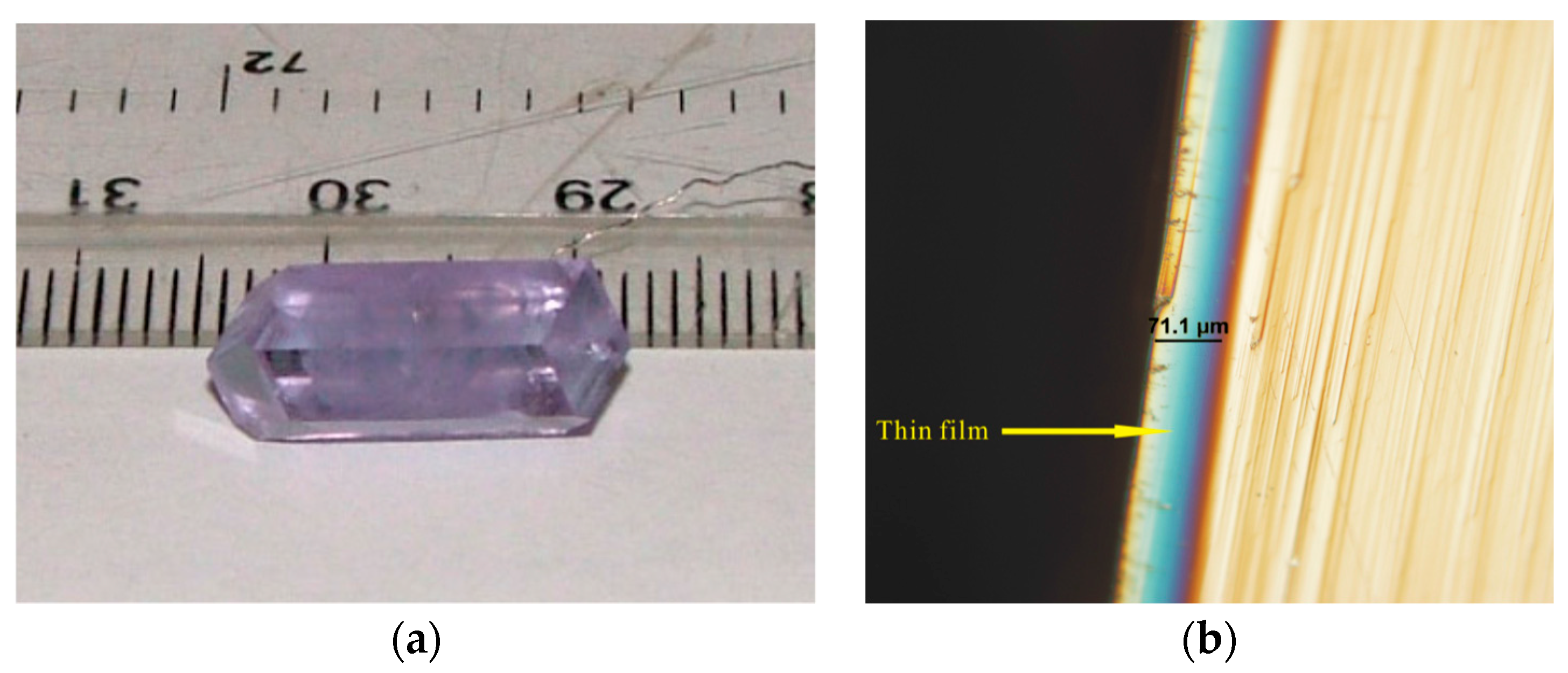
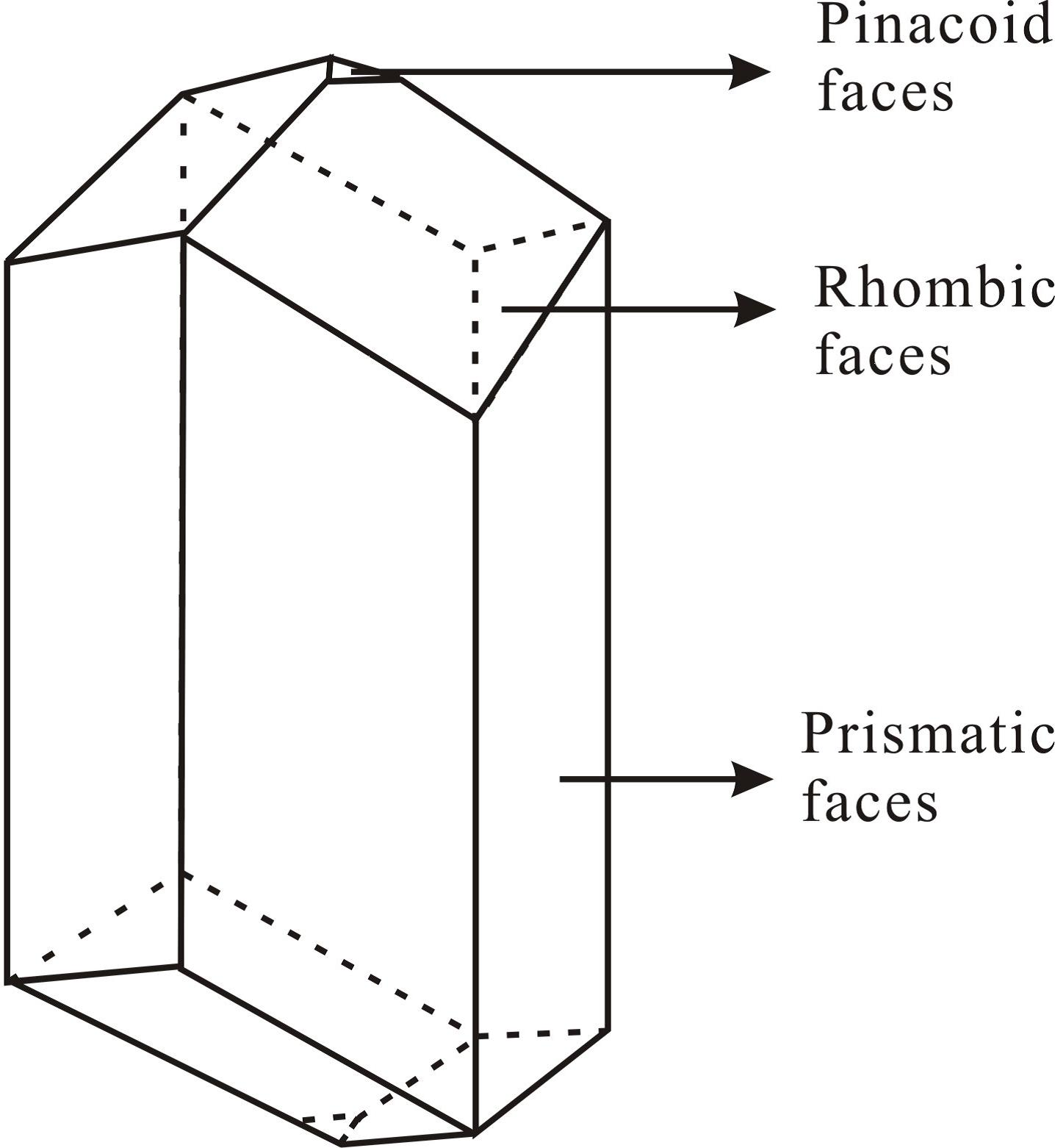
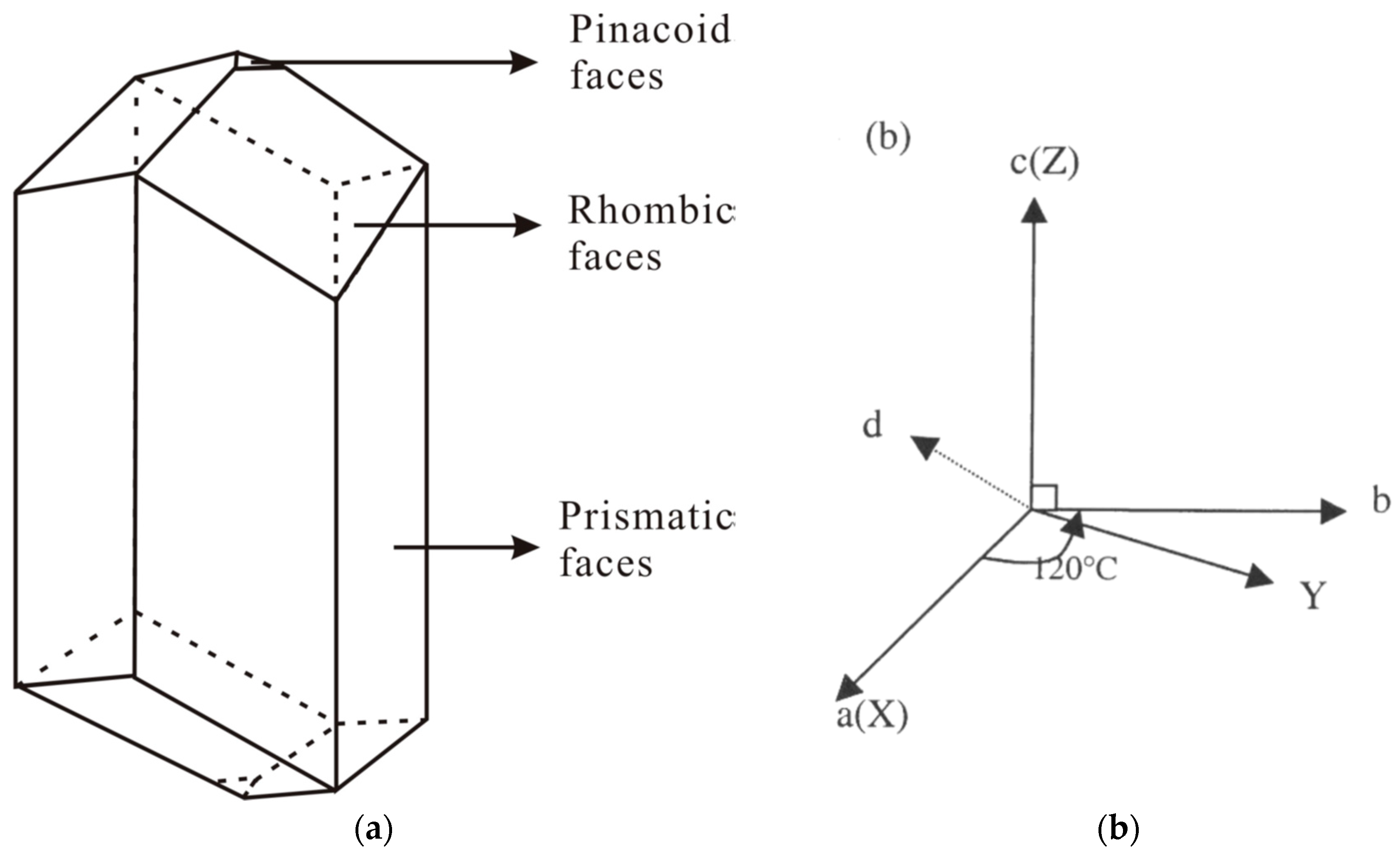
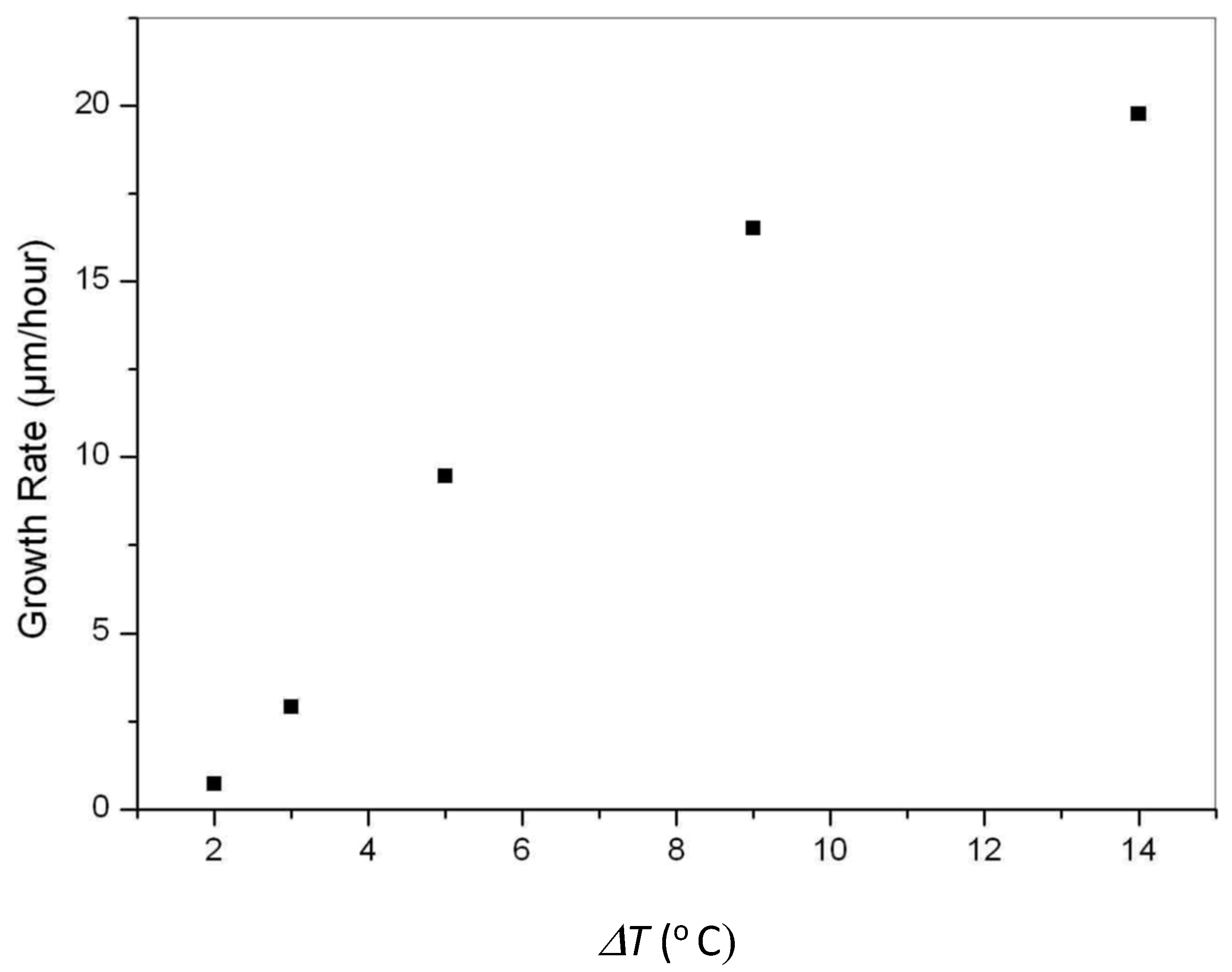
2.2. Results of Crystal Growth

Figure 3a shows an image of an as-grown Nd:YAB bulk crystal, with the growth facets visible, grown for two weeks under similar conditions as the thin films, with the temperature ramping down by 0.5 °C per day. Figure 3b shows an as-grown Nd:YAB crystalline thin film with un-doped YAB substrate that has been side-polished and imaged by a differential interference contrast microscope (Olympus BX60, Olympus Life Science, Sydney, Australia). The Nd:YAB thin film layer appears as a uniform, smooth blue stripe in the microscope image with a sharp change and an apparent phase contrast with the pure YAB substrate, which suggests a step-like refractive index profile. The film thickness was measured to be 71 ± 0.5 μm. The film shown in Figure 3b was obtained after epitaxial growth for 12 h at the conditions specified above. The as-grown thin film sample was transparent and homogeneous with a smooth surface. No noticeable crystallites of the monoclinic form of Nd:YAB were obtained, as discussed in Ref [35]. We attribute this to the moderate Nd dopant fraction and the lower temperature growth process that we used.

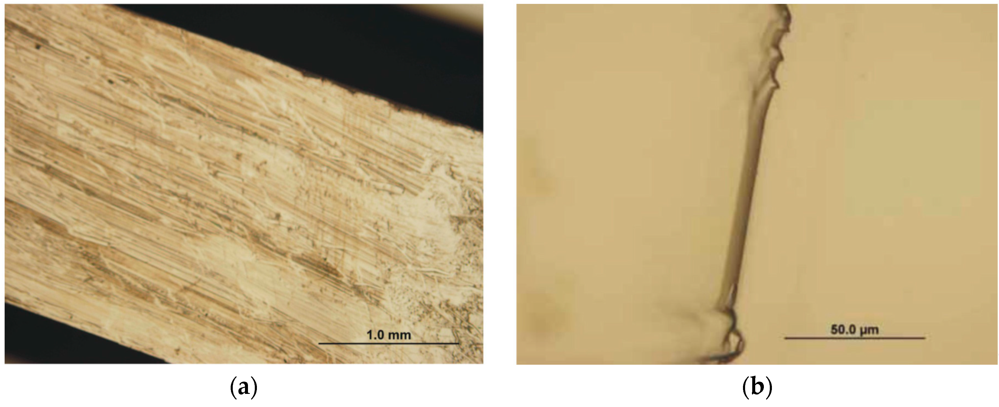
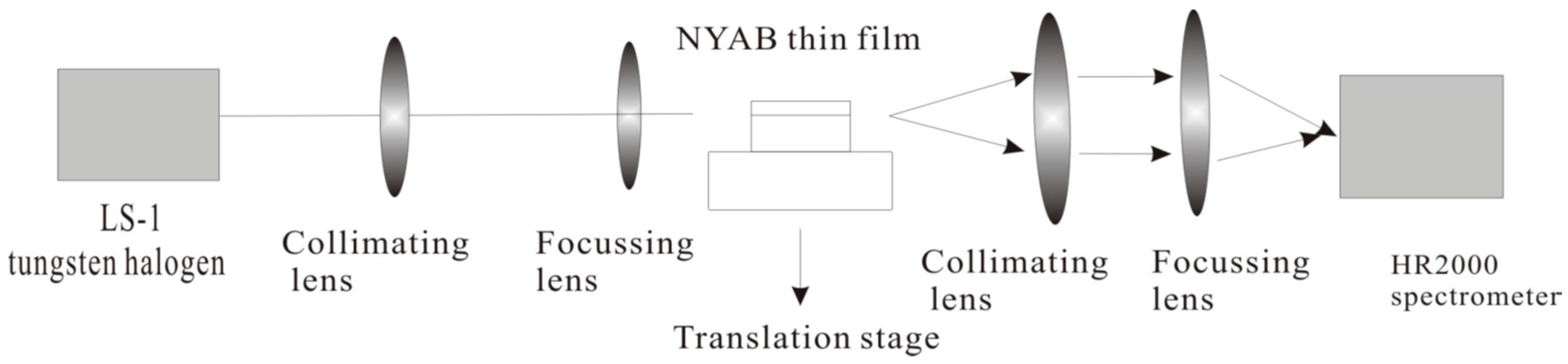
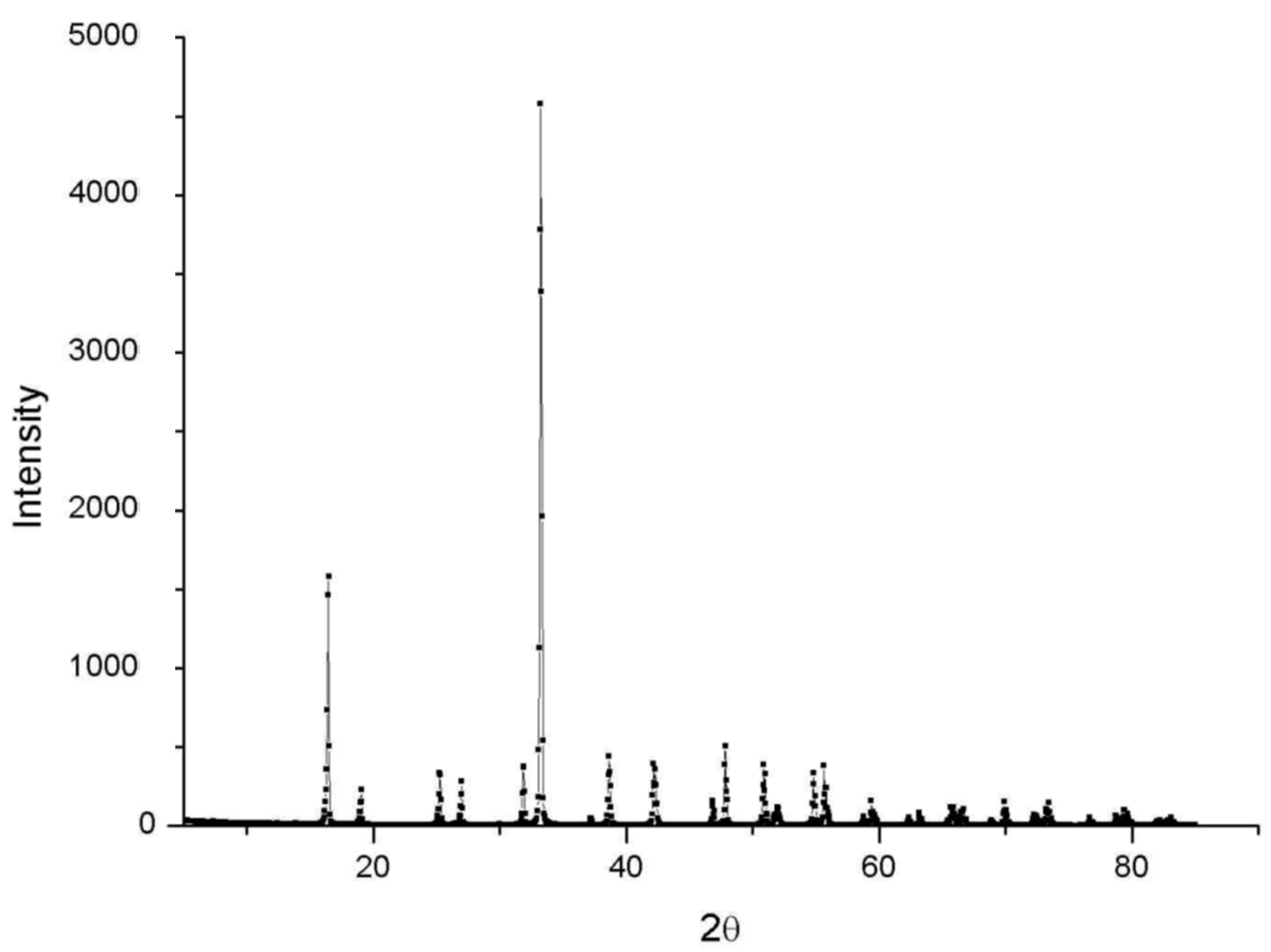
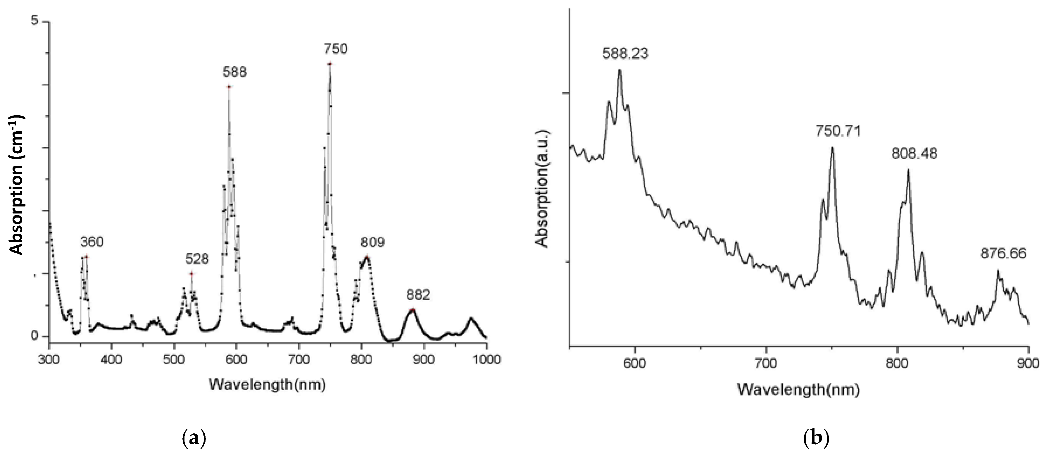
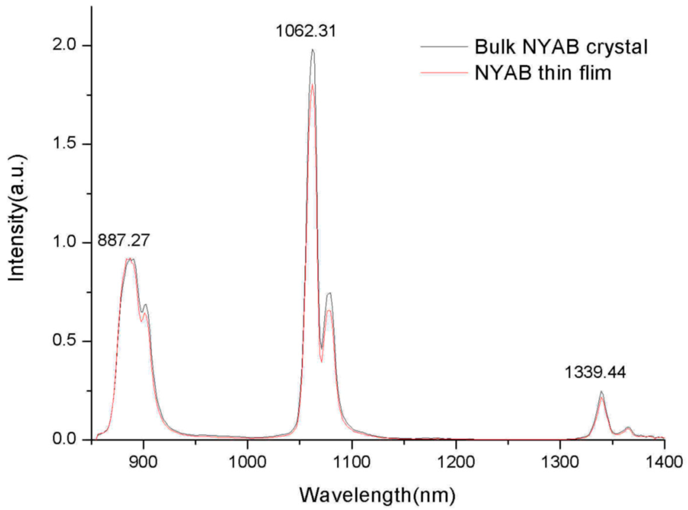
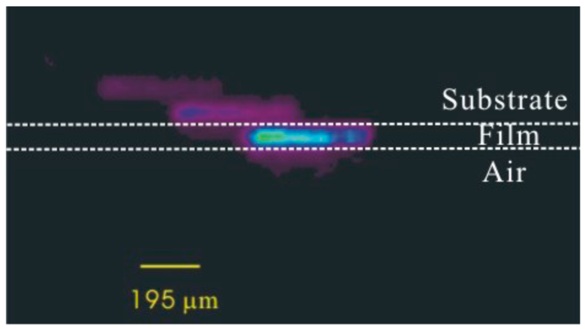
3. Crystal Characterization Methods and Results

Crystal Characterization Results

X-ray powder diffraction was used to characterise the crystallographic structure, and the results were compared with the diffraction patterns in an existing database. The X-ray powder diffraction (XRD) pattern of ground Nd:YAB bulk crystals grown by top-seeded solution growth was measured using a D/max-rA type X-ray diffractometer (Rigaku, Rigaku Americas Corp, The Woodlands, TX USA) with CuKα radiation (λ = 1.54056 Å) at room temperature, and is shown in Figure 4. The X-ray powder diffraction pattern of the Nd:YAB crystals was found to be consistent with the reference pattern of YAl3(BO3)4 and (JCPDS card No. 15-117) [37], indicating that the neodymium dopant does not significantly perturb the lattice and the crystal belongs to the R32 space group. The lattice parameters were calculated by the least-squares method.
According to the X-ray diffraction data, the calculated lattice constants of the Nd:YAB crystals were a = b = 9.298 Å and c = 7.2406 Å. In comparison with the data presented in Ref [16], the measured lattice constants of the bulk Nd:YAB crystal were close to those of Nd0.09Y0.91Al3(BO3)4, which were 9.295 Å and 7.236 Å. Thus our crystal properties are consistent with 9 at. % N dopant concentration within experimental error. Lattice constants of YAB crystals with different dopants are listed in Table 1. Assuming that the thin film has a similar Nd concentration to that of the bulk crystal, the lattice mismatch of the as-grown Nd:YAB thin film is about 0.11% and 0.2% for the lattice constants a and c, respectively. From optical microscopy and visual inspection, the Nd dopant distribution in the film appeared uniform. This is expected, as the solute concentration does not vary significantly during thin film growth.
The substrate crystal surface quality is shown in Figure 5a before thin film growth, and it shows the rough unpolished surface, which was smoothed in the initial period at a higher melt temperature. Figure 5b shows the as-grown crystalline film image in cross-section. The epitaxial growth results in a smooth surface with no additional crystallite formation. For the purposes of crystal characterization, the absorption spectrum of a 2 mm × 4 mm × 1.1 mm slice cut and polished from a bulk Nd:YAB crystal was measured using a Cary 5E spectrophotometer. This was compared with the absorption along the guiding direction of the epitaxial layer, as measured in the set up shown in Figure 6. Figure 7a shows the (unpolarised) absorption spectrum of bulk Nd:YAB (thickness 1.1 mm) in the wavelength range 300–1000 nm. There are six main absorption peaks in the spectrum at 360, 528, 588, 750, 809, and 882 nm, which may be assigned according to Reference [16]. The uncorrected absorption spectrum for the thin film is illustrated in Figure 7b. The absorption peak positions and features are similar to those for the bulk sample. The drifting base line is attributed to the wavelength response of the detector in the Ocean Optics HR2000 spectrometer.
The near-infrared fluorescence spectra of the Nd:YAB thin film (thickness 71 μm), and a bulk Nd:YAB crystal sample at room temperature, are overlaid in Figure 8. This spectrum was obtained by coupling light from an 808 nm diode laser into the thin film and focussing the output by a lens into a fibre-coupled spectrometer. The 887 nm, 1062 nm and 1339 nm peaks correspond to the fluorescence of the 4F3/2 level into the 4I9/2, 4I11/2, and 4I13/2 multiplets, respectively. The room temperature fluorescence peak at 1062 nm is very strong, and the bandwidth (FWHM) of the 1062 nm peak is about 10 nm. The fluorescence spectrum of the thin film Nd:YAB crystal is well-correlated with that of the bulk Nd:YAB sample.
A near-field image of the Nd:YAB thin film luminescence emitted from the end of the waveguide, as longitudinally pumped by the 808 nm diode laser, is shown in Figure 9. This was captured by a CCD camera (Pulnix, JAI Pulnix, Sydney, Australia) through a 1064 nm band pass filter. The camera was coupled to a laser beam analyser (Spiricon LBA100A, Ophir-Spiricon Photonics, West North Logan, UT, USA). The luminescence image size is about 71 µm in the guided direction and 400 µm in the unguided direction. Two subsidiary images, probably due to back reflections, are also observable to the upper left. This image shows strong evidence of effective guiding within the epitaxial film layer.

4. Discussion and Conclusions

Nd:YAB planar waveguides with 9% Nd dopant were successfully grown by the top-seeded solution method from the K2Mo3O10 and B2O3 flux system. The growth rates were measured and the growth conditions and procedure were selected for high-quality film growth in the thermodynamic regime. Nd:YAB thin film layers were obtained at 4 °C below the saturation temperature, with a growth rate about 5 μm/h on an un-doped {01 1 ¯ 1} YAB substrate. The growth of the thin films occurred over about 12 h, with additional time for cooling. The as-grown thin films have good surface and optical quality and homogeneity, and exhibit effective waveguiding of the strong luminescence at 1062 nm. Future measurements of optical gain and transmission losses in the devices are planned.

Author Contributions

Conceptualization J.M.D. and Y.L.; crystal growth methods and experiments Y.L.; crystal characterization Y.L. and P.D.; writing J.M.D. and Y.L. with editing by P.D.; and project administration J.M.D.

Funding

The authors acknowledge funding support to establish the crystal growth and characterization facility by Macquarie University and the Australian Research Council.

Acknowledgments

The authors acknowledge valuable advice and discussions on crystal growth and flux preparation from Nikolay Leonyuk and Robert Feigelson. Leonyuk provided bulk YAB crystals, which were used as substrates for the thin film growth.

Conflicts of Interest

The authors declare no conflict of interest.

References

  1. Tien, P.K. Light waves in thin films and integrated optics. Appl. Opt. 1971, 10, 2395–2413. [Google Scholar] [CrossRef] [PubMed]
  2. Snyder, A.W.; Love, J. Optical Waveguide Theory; Chapman and Hall: London, UK, 1983; pp. 6–26. ISBN 0-412-24250-8. [Google Scholar]
  3. Mackenzie, J.I. Dielectric solid state planar waveguide lasers: A review. IEEE J. Sel. Top. Quantum Electron. 2007, 13, 626–637. [Google Scholar] [CrossRef]
  4. Chen, F.; Vazquez de Aldana, J.R. Optical waveguides in crystalline dielectric materials produced by femtosecond-laser micromachining. Laser Photonics Rev. 2014, 8, 251–275. [Google Scholar] [CrossRef]
  5. Ams, M.; Marshall, G.D.; Dekker, P.; Piper, J.A.; Withford, M.J. Ultrafast laser-written active devices. Laser Photonics Rev. 2009, 3, 535–544. [Google Scholar] [CrossRef]
  6. Honkanen, S.; West, B.R.; Tliniemi, S.; Madasamy, P.; Morrell, M.; Auxier, J.; Geraghty, D. Recent advances in ion exchanged glass waveguides and devices. Phys. Chem. Glass. Eur. J. Glass Sci. Technol. B 2006, 47, 110–120. [Google Scholar]
  7. Brown, C.T.A.; Bonner, C.L.; Warburton, T.J.; Shepherd, D.P.; Tropper, A.C.; Hanna, D.C.; Meissner, H.E. Thermally bonded planar waveguide lasers. Appl. Phys. Lett. 1997, 71, 1139–1141. [Google Scholar] [CrossRef]
  8. Capper, P.; Irvine, S.; Joyce, T. Epitaxial Crystal Growth: Methods and Materials. In Springer Handbook of Electronic and Photonic Materials; Springer Handbooks; Kasap, S., Capper, P., Eds.; Springer: Cham, Switzerland, 2017. [Google Scholar]
  9. Ferrand, B.; Chambaz, B.; Couchaud, M. Liquid phase epitaxy: A versatile technique for the development of miniature optical components in single crystal dielectric media. Opt. Mater. 1999, 11, 101–114. [Google Scholar] [CrossRef]
  10. Beecher, S.J.; Grant-Jacob, J.A.; Hua, P.; Prentice, J.J.; Eason, R.W.; Shepherd, D.P.; Mackenzie, J.I. Ytterbium-doped-garnet crystal waveguide lasers grown by pulsed laser deposition. Opt. Mater. Express 2017, 7, 1628–1633. [Google Scholar] [CrossRef]
  11. Cho, A.Y. Advances in Molecular Beam Epitaxy. J. Cryst. Growth 1991, 111, 1–13. [Google Scholar] [CrossRef]
  12. Terry, R.J.; McMillen, C.D.; Chen, X.; Wen, Y.; Zhu, L.; Chumanov, G.; Kolis, J.W. Hydrothermal single crystal growth and second harmonic generation of Li2SiO3, Li2GeO3, and Li2Si2O5. J. Cryst. Growth 2018, 493, 58–64. [Google Scholar] [CrossRef]
  13. Sun, H.; Li, K.H.; Torres Castanedo, C.G.; Okur, S.; Tompa, G.S.; Salagaj, T.; Lopatin, S.; Genovese, A.; Li, X. HCl Flow-Induced Phase Change of α-, β-, and ε-Ga2O3 Films Grown by MOCVD. Cryst. Growth Des. 2018, 18, 2370–2376. [Google Scholar] [CrossRef]
  14. Tassev, V.; Vangala, S.; Peterson, R.; Kimani, M.; Snure, M.; Markov, I. Homo and heteroepitaxial growth and study of orientation-patterned GaP for nonlinear frequency conversion devices. Proc. SPIE 2016, 9731, 97310G, “Nonlinear Frequency Generation and Conversion: Materials, Devices, and Applications XV, (4 March 2016); Vodopyanov, K.L.; Schepler, K.L.; Eds”. [Google Scholar] [CrossRef]
  15. Ballman, A.A. A new series of synthetic borates isostructural with the carbonate mineral huntite. Am. Mineral. 1962, 47, 1380–1383. [Google Scholar]
  16. Leonyuk, N.I.; Leonyuk, L.I. Growth and characterization of RM3(BO3)4 crystals. Prog. Cryst. Growth Charact. 1995, 31, 179–278. [Google Scholar] [CrossRef]
  17. Wang, P.; Dawes, J.M.; Dekker, P.; Knowles, D.S.; Piper, J.A.; Lu, B.S. Growth and evaluation of ytterbium doped yttrium aluminum borate as a potential self-doubling laser crystal. J. Opt. Soc. Am. B 1999, 16, 63–69. [Google Scholar] [CrossRef]
  18. Jaque, D.; Enguita, O.; Garcia Sole, J.; Jiang, A.D.; Luo, Z.D. Infrared continuous wave laser gain in neodymium aluminum borate: A promising candidate for microchip diode-pumped solid-state lasers. Appl. Phys. Lett. 2000, 76, 2176–2178. [Google Scholar] [CrossRef]
  19. Wang, P.; Dekker, P.; Dawes, J.M.; Piper, J.A.; Liu, Y.G.; Wang, J.Y. Efficient continuous wave self-frequency doubling green diode pumped Yb:YAB lasers. Opt. Lett. 2000, 25, 731–733. [Google Scholar] [CrossRef] [PubMed]
  20. Dekker, P.; Dawes, J.M.; Piper, J.A.; Liu, Y.G.; Wang, J.Y. 1.1W CW self-frequency doubled diode-pumped Yb:YAl3(BO3)4 laser. Opt. Commun. 2001, 195, 431–436. [Google Scholar] [CrossRef]
  21. Lederer, M.J.; Hildebrandt, M.; Kolev, V.Z.; LutherDavies, B.; Taylor, B.; Dawes, J.M.; Dekker, P.; Piper, J.A.; Tan, H.H.; Jagadish, C. Passive mode locking of a self-frequency doubling Yb:YAl3(BO3)4 laser. Opt. Lett. 2002, 27, 436–438. [Google Scholar] [CrossRef]
  22. Dekker, P.; Dawes, J.M.; Piper, J.A. 2.27 W Q-switched self-doubling Yb:YAB laser with controllable pulse length. J. Opt. Soc. Am. B 2005, 22, 378–384. [Google Scholar] [CrossRef]
  23. Chen, Y.J.; Lin, Y.F.; Gong, X.H.; Tan, Q.G.; Luo, Z.D.; Huang, Y.D. 2.0 W diode-pumped Er,Yb:YAl3(BO3)4 efficient 1.5 m laser crystal. Appl. Phys. Lett. 2006, 89, 241111. [Google Scholar] [CrossRef]
  24. Lagatsky, A.A.; Sibbett, W.; Kisel, V.E.; Troshin, A.E.; Tolstik, N.A.; Kuleshov, N.V.; Leonyuk, N.L.; Zhukov, A.E.; Rafailov, E.U. Diode-pumped passively mode locked Er,Yb:YAl3(BO3)4 laser at 1.5–1.6 m. Opt. Lett. 2008, 33, 83–85. [Google Scholar] [CrossRef] [PubMed]
  25. Blows, J.L.; Dekker, P.; Wang, P.; Dawes, J.M.; Omatsu, T. Thermal lensing measurements and thermal conductivity of Yb:YAB. Appl. Phys. B 2003, 76, 289–292. [Google Scholar] [CrossRef]
  26. Liu, J.; Mateos, X.; Zhang, H.J.; Li, J.; Wang, J.Y.; Petrov, V. High power laser performance of Yb:YAl3(BO3)4 crystals cut along the crystallographic axes. IEEE J. Quantum Electron. 2007, 43, 385–390. [Google Scholar] [CrossRef]
  27. Weichelt, B.; Rumpet, M.; Voss, A.; Wesemann, V.; Rytz, D.; Abdou Ahmed, M.; Graf, T. Yb:YAl3(BO3)4 as gain material in thin disk oscillators: Demonstration of 109 W of IR output power. Opt Expr. 2013, 21, 25709. [Google Scholar] [CrossRef] [PubMed]
  28. Yu, X.; Yue, Y.; Yao, J.; Hu, Z.G. YAl3(BO3)4 crystal growth and characterization. J. Cryst. Growth 2010, 312, 3029–3033. [Google Scholar] [CrossRef]
  29. Yu, J.; Liu, L.; Zhai, N.; Zhang, X.; Wang, G.; Wang, X.; Chen, C. Crystal growth and optical properties of YAl3(BO3)4 for UV applications. J. Cryst. Growth 2012, 341, 61–65. [Google Scholar] [CrossRef]
  30. Dekker, P.; Dawes, J.M. Characterisation of nonlinear conversion and crystal quality in Nd and Yb doped YAB. Opt. Expr. 2004, 12, 5922–5930. [Google Scholar] [CrossRef]
  31. Dekker, P.; Dawes, J.M. Twinning and natural quasi-phase matching in Yb:YAB. Appl. Phys. B 2006, 83, 267. [Google Scholar] [CrossRef]
  32. Lutz, F.; Leiss, M.; Muller, J. Epitaxy of NdAl3(BO3)4 for thin film miniature lasers. J. Cryst. Growth 1979, 47, 130–132. [Google Scholar] [CrossRef]
  33. Volkova, E.; Leonyuk, N. Growth of Yb:YAl3(BO3)4 thin films by liquid-phase epitaxy. J. Cryst. Growth 2005, 275, e2467–e2470. [Google Scholar] [CrossRef]
  34. Volkova, E.; Markin, V.; Leonyuk, N.I. High temperature growth and characterization of (Er,Yb):YAl3(BO3)4 single crystal layers. J. Cryst. Growth 2017, 468, 258–261. [Google Scholar] [CrossRef]
  35. Volkova, E.; Maltsev, V.; Kolganova, O.; Leonyuk, N.I. High temperature growth and characterization of Er,Yb:YAl3(BO3)4 and NdAl3(BO3)4 epitaxial layers. J. Cryst. Growth 2014, 401, 547–549. [Google Scholar] [CrossRef]
  36. Tolstik, N.; Heinrich, S.; Kahn, A.; Volkova, E.; Maltsev, V.; Kuleshov, V.; Huber, G.; Leonyuk, N.I. High temperature growth and spectroscopic characterization of Er,Yb:YAl3(BO3)4 epitaxial thin layers. Opt. Mater. 2010, 32, 1377–1379. [Google Scholar] [CrossRef]
  37. Mills, A.D. Crystallographic data for new rare earth borate compounds RX3(BO3)4. Inorg. Chem. 1962, 1, 960–961. [Google Scholar] [CrossRef]
Figure 1. (a) The growth habit of Nd:YAB crystals and (b) the hexagonal crystal axes for the crystals.
Crystals 09 00079 g001
Figure 2. Nd:YAB crystal growth rate on the rhombic face seed crystal versus temperature below saturation ΔT (°C).
Crystals 09 00079 g002
Figure 3. (a) As-grown bulk Nd:YAB crystal and (b) differential interference contrast image of the Nd:YAB thin film and YAB substrate in cross-section.
Crystals 09 00079 g003
Figure 4. X-ray powder diffraction for as-grown Nd:YAB crystal.
Crystals 09 00079 g004
Figure 5. (a) Microscope images of substrate surface (5×) and (b) after growth thin film surface (20×) for Nd:YAB on a YAB substrate. The substrate is held vertically in the flux.
Crystals 09 00079 g005
Figure 6. Experimental setup for measuring absorption spectra along guiding direction.
Crystals 09 00079 g006
Figure 7. (a) Absorption spectrum of a polished slice of bulk Nd:YAB and (b) uncorrected absorption spectrum of Nd:YAB crystalline thin film, along the guiding direction, showing intensity peaks at 588, 750 and 808 nm, attributed to transitions from 4I9/2 to 4G5/2, 4F7/2 and 2H9/2, respectively.
Crystals 09 00079 g007
Figure 8. Luminescence spectrum of Nd:YAB thin film overlaid with that of the bulk Nd:YAB sample.
Crystals 09 00079 g008
Figure 9. Luminescence image of Nd:YAB thin film (image artefacts to the upper left).
Crystals 09 00079 g009
Table 1. Lattice parameters of YAl3(BO3)4.
Crystalsa (Å)c (Å)Reference
YAB (JCPDS No. 15-117)9.28727.2433[37]
Nd0.09Y0.91Al3(BO3)49.2957.236[16]
NdAl3(BO3)49.3657.262[16]
Nd:YAB crystal9.2987.2406This work

