Article

Hysteresis Reduction for Organic Thin Film Transistors with Multiple Stacked Functional Zirconia Polymeric Films

1
School of Electronics Engineering, Kyungpook National University, Daegu 41566, Korea
2
Department of Electronic Engineering, Hallym University, Chuncheon 24252, Korea
*
Authors to whom correspondence should be addressed.
Crystals 2019, 9(12), 634; https://doi.org/10.3390/cryst9120634
Submission received: 4 November 2019 / Revised: 24 November 2019 / Accepted: 27 November 2019 / Published: 28 November 2019
(This article belongs to the Special Issue Advances in Thin Film Materials and Devices)

Abstract

:
We show that transfer hysteresis for a pentacene thin film transistor (TFT) with a low-temperature solution-processed zirconia (ZrOx) gate insulator can be remarkably reduced by modifying the ZrOx surface with a thin layer of crosslinked poly(4-vinylphenol) (c-PVP). Pentacene TFTs with bare ZrOx and c-PVP stacked ZrOx gate insulators were fabricated, and their hysteresis behaviors compared. The different gate insulators exhibited no significant surface morphology or capacitance differences. The threshold voltage shift magnitude decreased by approximately 71% for the TFT with the c-PVP stacked ZrOx gate insulator compared with the bare ZrOx gate insulator, with 0.75 ± 0.05 and 0.22 ± 0.03 V threshold voltage shifts for the bare ZrOx and c-PVP stacked ZrOx gate insulators, respectively. The hysteresis reduction was attributed to effectively covering hysteresis-inducing charge trapping sites on ZrOx surfaces.

Graphical Abstract

1. Introduction

Combined metal oxide and organic layers have been extensively studied for research and practical applications [1,2,3], providing key functional materials for next-generation electronics. Applications for metal oxides and organic compounds encompass a wide range of electronic components including thin film transistors (TFTs), light emitting diodes, photovoltaic cells, and biochemical sensors [4,5,6]. One of their most critical features is solution processability, which offers facile low-cost large area production for electronics compared with conventional vacuum processes. Solution processes commonly incorporate sol-gel methods [7]. Diverse metal oxides and organic compounds for electronic applications have been previously demonstrated to provide high optical transparency in the visible region and mechanical flexibility [8,9]. Thus, combined metal oxide and organic layers may provide new concepts for electronics incorporating flexibility, transparency, and other significant technological advantages.
One example application for combined metal oxide and organic layers is gate insulators and active layers for organic TFTs [10]. TFTs are critical components of electronic circuits in displays and sensors, and zirconia (ZrOx), hafnia, yttria, and titania films are attractive candidates for low-voltage organic TFT gate insulators [11,12]. ZrOx offers a good option for organic TFTs due to its solution processability, large band gap, high permittivity, low leakage current, and thermal and mechanical stability [12,13]. One facile sol-gel method for obtaining high-quality defect-minimized ZrOx films is high-temperature annealing, since sol-gel methods are generally based on a series of chemical reactions requiring specific activation energies. However, high-temperature annealing is not suitable for flexible electronics, which are built on plastic substrates with relatively low thermal resistance, since most plastic substrates are severely damaged by process temperatures above 200 °C [14]. Thus, eliminating defects and related effects in low-temperature solution-processed ZrOx films is essential for flexible electronics applications.
Previous studies have shown that TFTs with solution-processed ZrOx gate insulators often exhibit low electrical stability, e.g., large transfer hysteresis [15,16,17]. Interfacial properties between gate insulators and active layers are crucial for TFT electrical characteristics; hence, gate insulator surface properties can greatly affect hysteresis. Therefore, low-temperature solution-processed ZrOx gate insulators need improved TFT hysteresis characteristics. For example, covering ZrOx gate insulators with thin polymeric layers may provide improved interfaces by preventing hysteresis-inducing factors present on the surfaces from forming direct contacts with TFT channels. Although bilayer gate insulators are commonly employed for TFT hysteresis reduction, surface modification of low-temperature solution-processed ZrOx films with polymeric layers has not yet been explored in the context of TFT hysteresis.
This study fabricated pentacene TFTs with bare zirconia (ZrOx) and crosslinked poly(4-vinylphenol) (c-PVP) stacked ZrOx gate insulators and analyzed their hysteresis behaviors. Cross-sectional and surface morphologies for bare and c-PVP stacked ZrOx thin films were examined by scanning electron microscopy (SEM) and atomic force microscopy (AFM), and water contact angles were measured. Morphological properties for pentacene thin films thermally deposited on bare and c-PVP stacked ZrOx thin films were examined by AFM, and their crystalline properties by X-ray diffraction (XRD). Metal–insulator–metal (MIM) capacitor capacitances were also measured.

2. Materials and Methods

We produced ZrOx solution by dissolving 40 mg/mL zirconium (IV) acetylacetonate (487.66 g/mol, Sigma Aldrich) in methanol (32.04 g/mol, Sigma Aldrich) [18], and added monoethanolamine (61.08 g/mol, Sigma Aldrich) as a stabilizer, i.e., molar ratio 1:1 between zirconium (IV) acetylacetonate and monoethanolamine. The ZrOx solution was stirred at 50 °C for 12 hours. To produce c-PVP solution, we dissolved PVP (25,000 g/mol, Sigma Aldrich) in propylene glycol methyl ether acetate (132.16 g/mol, Sigma Aldrich) at 0.1 wt%, and then added methylated poly(melamine-co-formaldehyde) (432.84 g/mol, Sigma Aldrich) at a 1:1.125 weight ratio as a crosslinking agent [19]. The PVP solution was stirred at room temperature for 12 hours.
Top-contact bottom-gate pentacene TFTs with bare and c-PVP stacked ZrOx thin gate insulators were fabricated, and 50 nm aluminum films were thermally evaporated on cleaned glass substrates through a shadow mask at a 0.1 nm/s deposition rate, and bare and c-PVP stacked ZrOx thin films were formed on the substrates. ZrOx solution was spin coated onto the substrate at 3000 rpm with subsequent soft and hard bake two-step thermal treatment. Soft bake samples were annealed on a hotplate at 65 °C for 10 minutes, whereas hard bake samples were annealed on a hotplate at 200 °C for 1 hour in a moisture-rich environment, created by vaporizing water from a reservoir at 7 mg/min. To form c-PVP stacked ZrOx gate insulators, PVP solution was spin-coated on pre-formed ZrOx film at 3000 rpm with subsequent thermal treatment on a hot plate at 200 °C to crosslink PVP chains. Then, 50 nm pentacene (278.35 g/mol, Sigma Aldrich) films were thermally evaporated on the gate insulators at a 0.1 nm/s deposition rate to form active layers. Finally, source/drain electrodes were fabricated by thermally evaporating 50 nm gold films onto the pentacene films through a shadow mask at a 0.1 nm/s deposition rate, creating channels with length L = 50 μm and width W = 400 μm. In addition, two MIM construction capacitors were fabricated using bare and c-PVP stacked ZrOx thin films. Aluminum films (50 nm) were deposited by thermal evaporation to form bottom and top electrodes for the MIM capacitors. All deposition processes were conducted at 1.6 × 10⁻⁶ Torr base pressure.
Electrical characterization for the pentacene TFTs was performed using the EL420C semiconductor parameter analyzer (ELECS, Seoul, South Korea), and MIM capacitor capacitances were measured using the HP4192A impedance analyzer (Hewlett Packard, San Jose, CA, USA). SEM, AFM, and XRD measurements for thin films were performed using S-4800 (Hitachi High-Technologies, Tokyo, Japan), NX20 (Park Systems, Suwon, South Korea), and D/Max-2500 (Rigaku, Tokyo, Japan), respectively.

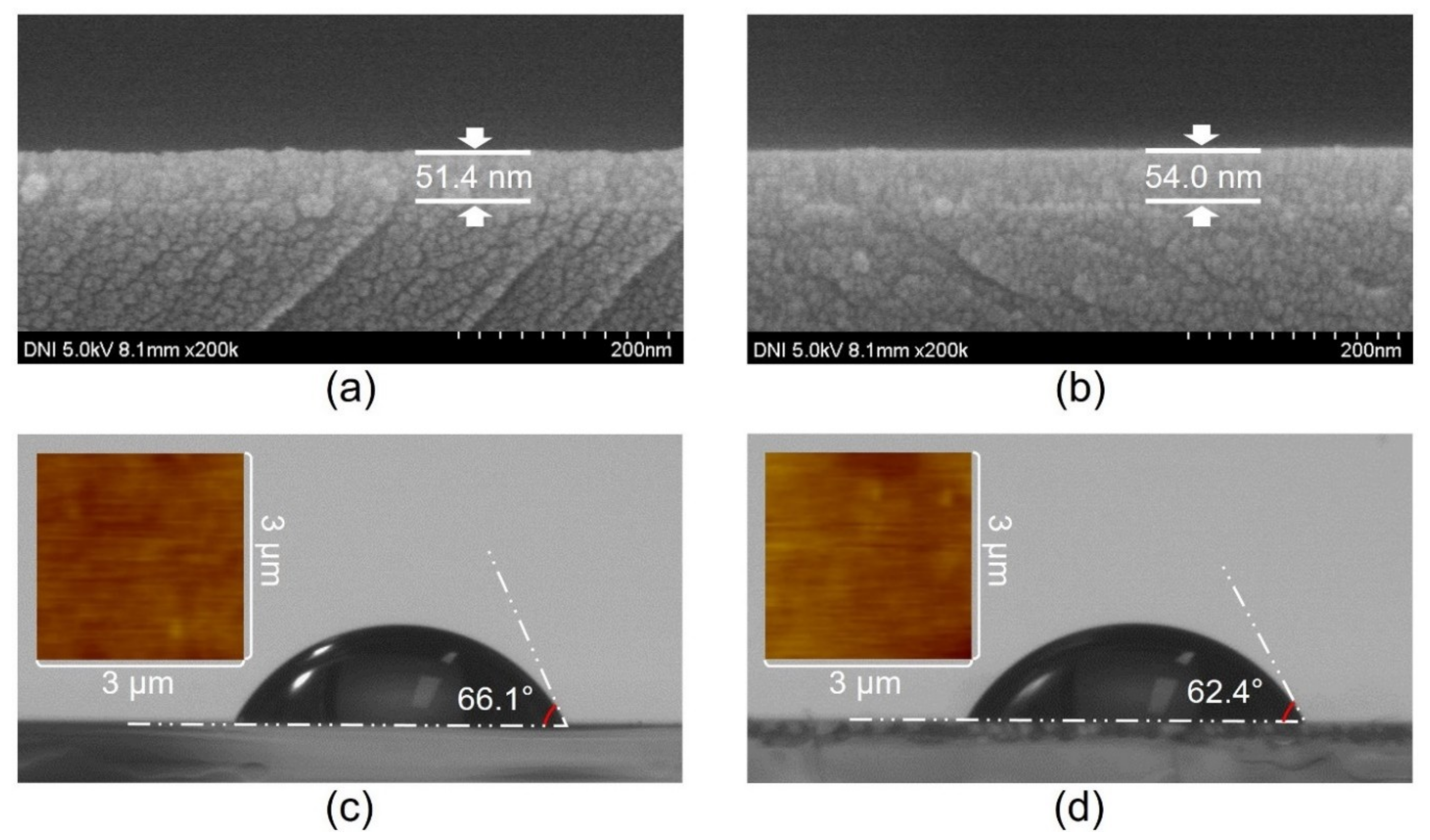
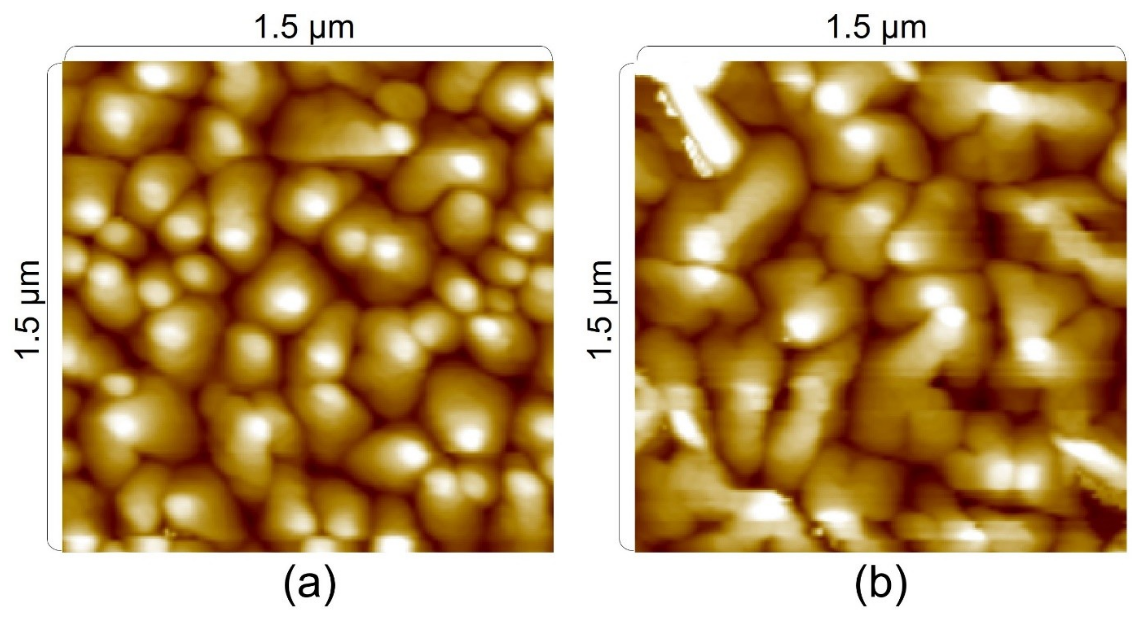
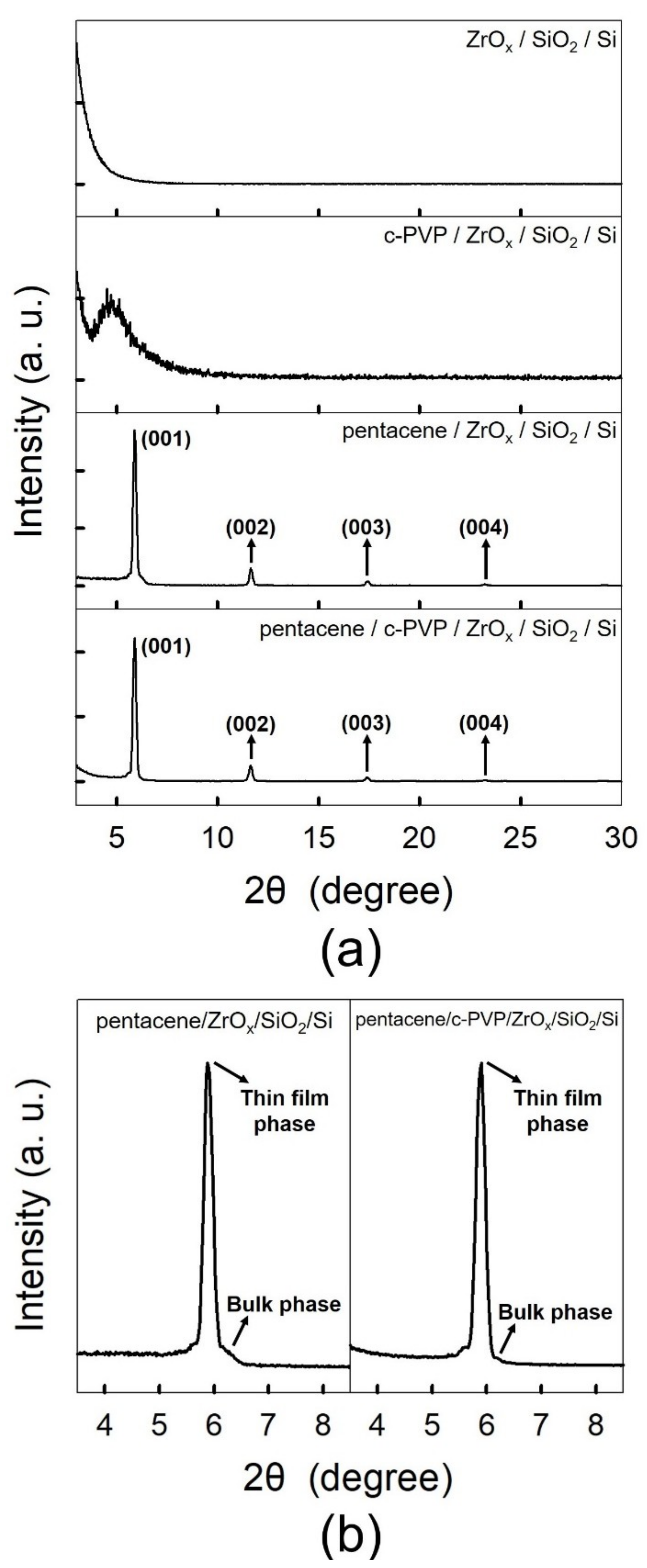
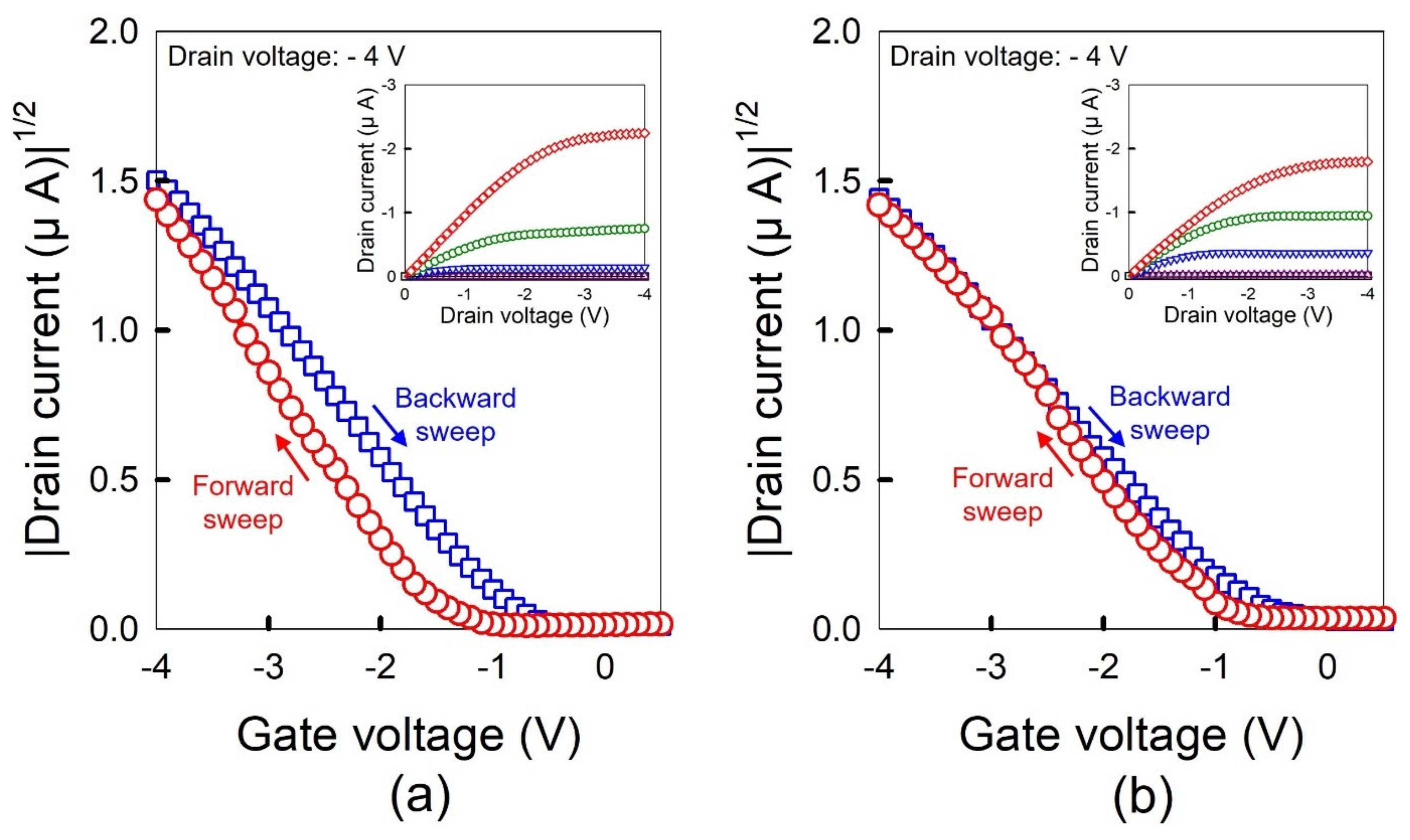
3. Results and Discussion

Figure 1a,b show typical cross-sectional SEM surface images for bare and c-PVP stacked ZrOx thin films. The thin films exhibited thicknesses of approximately 51.4 and 54 nm, respectively, indicating that the stacked c-PVP layer was approximately 2.6 nm. Figure 1c,d show water contact angles on bare and c-PVP stacked ZrOx thin films. The measured contact angles ≈ 66.1° and 62.4°, respectively. We calculated surface energies (γPs) for the bare and c-PVP stacked ZrOx thin films as
γ P = γ W 4 ( 1 + cos θ 0 ) 2
where γW = 73.0 mJ/m2 is the surface free energy for water, and θ0 is the contact angle at equilibrium [20]. Thus, γPs ≈ 36.0 and 39.1 mJ/m2 for bare and c-PVP stacked ZrOx thin films, respectively, i.e., the c-PVP stacked ZrOx thin film exhibited a higher γP than the bare ZrOx thin film. The different γP between the bare ZrOx and c-PVP stacked ZrOx thin films is related to their different chemical states. Figure 1c,d insets show typical surface AFM images (3 × 3 μm) for bare and c-PVP stacked ZrOx thin films, respectively. The thin films exhibit comparable surface morphologies and root-mean-square surface roughness; approximately 0.162 and 0.171 nm, respectively. Structural defects, such as pinholes, were not observed in the AFM analyses, which indicates that the gate stack quality was sufficiently high for both bare ZrOx and c-PVP stacked ZrOx thin films.
Figure 2a,b show typical surface AFM images (1.5 × 1.5 μm) for pentacene thin films thermally deposited on bare and c-PVP stacked ZrOx thin films, respectively. The thin films exhibit an approximate surface roughness equal to 6.55 and 7.72 nm, respectively. The pentacene on the c-PVP stacked ZrOx thin film exhibited more dendritic and larger grains than that on the bare ZrOx thin film. The relatively high γP for c-PVP stacked ZrOx thin films can affect pentacene layer-by-layer growth, yielding relatively larger grains [21].
Figure 3a shows typical XRD patterns for bare and c-PVP stacked ZrOx thin films with thermally deposited pentacene thin films. There were no discernible sharp XRD peaks in either case, indicating that they were formed in amorphous states. All pentacene thin films exhibited (001), (002), (003), and (004) peaks, which agrees well with the typical (00l) pattern for pentacene thin film phase crystallites [22]. Figure 3b shows the (001) diffraction peaks for the pentacene thin films. Examination of (001) diffraction peaks provides critical information on the molecular state of pentacene thin films [23]. The pentacene thin films exhibited similar full width at half maximum (FWHM) values for the (001) peaks, approximately 0.191 ± 0.001°. Since the XRD peak FWHM for organic films is associated with their crystallinity [24], the similar FWHM values suggest comparable crystallinity between the pentacene thin films. The pentacene thin films exhibited similar (001) interlayer spacing values, approximately 1.499 ± 0.001 nm, which were calculated by Bragg’s Law (λ = 2dhkl sin(θ)) [25]. In addition, as shown in Figure 3b, the pentacene thin film deposited on the c-PVP stacked ZrOx thin film exhibited a relatively lower bulk-to-thin film phase XRD intensity ratio than the one deposited on bare ZrOx film. This indicates that the pentacene thin film on the c-PVP stacked ZrOx thin film has a lower density of bulk phase crystallites than that on the bare ZrOx thin film [23]. The variation in the pentacene phase state is related to the different chemical states and γP between bare ZrOx and c-PVP stacked ZrOx thin films.
The MIM capacitor capacitances were measured by applying a small alternating current (AC) signal (10 mV at 100 kHz). MIM capacitors with a c-PVP stacked ZrOx thin film exhibited a comparable but slightly lower capacitance than those with a bare ZrOx thin film (approximately 74.7 and 79.4 nF/cm2, respectively). The calculated capacitance for MIM capacitors with a c-PVP stacked ZrOx film was 74.8 nF/cm2, from the usual series capacitance relationship, which agrees well with the measured value (74.7 nF/cm2). In addition, the dielectric constant of the bare ZrOx thin film was 4.61, and the average dielectric constant of the c-PVP stacked ZrOx thin film was 4.55. It worth noting that the dielectric constant of ZrOx thin film (=4.61) is higher than that for c-PVP (=3.9) and conventional SiO2 (=3.9), since different dipole–channel interactions may lead to different TFT characteristics.
Figure 4a,b show transfer characteristics for pentacene TFTs with bare and c-PVP stacked ZrOx gate insulators, respectively, measured by varying the gate voltage (VG) from 0.5 to −4 V and back in 0.5 V increments and 0.1 V decrements at constant VD = −4 V. Since drain current is
I D = W μ e f f C o x 2 L ( V G V T ) 2
where Cox is the gate insulator capacitance and VT is the threshold voltage [26], we extracted field-effect mobilities (μFEs) from the slope of |ID|1/2 with respect to VG. The pentacene TFTs exhibited comparable μFE values (1.02 ± 0.06 cm2/Vs). The Figure 4a,b insets show output characteristics for pentacene TFTs with bare and c-PVP stacked ZrOx gate insulators, respectively, measured by changing drain voltage (VD) from 0 V to −4 V in 0.1 V increments at different VGs (VG = 0, −1, −2, −3, and −4 V). All devices exhibited a linear ID increase for small VD and ID saturation for high VD. All devices were operated in p-channel accumulation mode.
There were remarkable hysteresis differences between pentacene TFTs with the two gate insulator types. Transfer hysteresis is an important parameter for TFT electrical stability [27]. We extracted VT by linear extrapolation from |ID|1/2 versus VG plots to ID = 0; VT,forward = −1.60, VT,backward = −0.85 V for the bare ZrOx case; and VT,forward = −0.98, VT,backward = −0.76 V for the c-PVP stacked ZrOx case. The TFT with the c-PVP stacked ZrOx gate insulator exhibited a smaller VT magnitude than that with the bare ZrOx gate insulator. In particular, VT,hysteresis = VT,backwardVT,forward = 0.75 ± 0.05 and 0.22 ± 0.03 V for the bare and c-PVP stacked ZrOx cases, respectively. VT,hysteresis decreased by approximately 71% for the TFT with the c-PVP stacked ZrOx gate insulator compared with the bare ZrOx gate insulator. Note that a TFT channel was formed at the gate insulator/semiconductor interface. The relatively smaller VT,hysteresis for the c-PVP stacked ZrOx case indicates that c-PVP stacked ZrOx gate insulator and pentacene film interfaces had a lower number of charge-trapping sites than bare ZrOx gate insulator and pentacene films did, since VT,hysteresis magnitude is directly dependent on the quantity of charge trapped during hysteresis. Sol-gel solution-processed metal oxide thin films often suffer from various defects, including Schottky and Frenkel defects, residual hydroxyl groups and ligands, and various byproducts [28]. Due to the high possibility for the presence of such diverse defects, we consider that solution-processed bare ZrOx gate insulators created more defect-induced charge-trapping sites at pentacene film interfaces, whereas c-PVP layer defects were limited to mainly residual hydroxyl groups, inducing less interfacial charge-trapping sites [19]. Moreover, high-k ZrOx dipoles, strongly interacting with TFT channel charge carriers, possibly contributed to the TFT hysteresis. Covering the ZrOx gate insulator with a c-PVP layer provided an improved interface by preventing surface charge-trapping sites from forming a direct contact with the TFT channel. Consequently, the c-PVP stacked ZrOx gate insulator led to significantly reduced hysteresis in pentacene TFTs.
Further study is needed to identify the fundamental hysteresis mechanisms through optical and thermal analyses, and theoretical calculations for individual defect species. Moreover, devising methods of modifying the ZrOx dielectric constant and bandgap will be important for further advancement of ZrOx. The current study regarding low-temperature solution-processed ZrOx films in organic TFTs provides a significant step towards developing flexible and transparent electronics.

4. Conclusions

We showed that transfer hysteresis for a pentacene TFT with a low-temperature solution-processed ZrOx gate insulator was remarkably reduced by modifying the ZrOx surface with a thin c-PVP layer. This study compared hysteresis behaviors for pentacene TFTs with bare and c-PVP stacked ZrOx gate insulators. We found VT,hysteresis = 0.75 ± 0.05 and 0.22 ± 0.03 V for bare and c-PVP stacked ZrOx thin films, respectively. MIM capacitors exhibited a comparable capacitance for bare and c-PVP stacked ZrOx thin films (79.4 and 74.7 nF/cm2, respectively). Pentacene TFTs exhibited a comparable μFE (1.02 ± 0.06 cm2/V/s) for both thin film types. These results provide useful background to improve electrical stability for next-generation electronics incorporating combined metal oxide and organic layers.

Author Contributions

Conceptualization, J.-H.B. and J.P.; Formal analysis, J.-H.K., J.-H.C., J.-H.B., and J.P.; Investigation, J.-H.K. and J.-H.C.; Methodology, J.-H.K., J.-H.B., and J.-H.P.; Writing—original draft, J.-H.K.; Writing—review & editing, J.-H.K., J.-H.B., and J.P.

Funding

This research was funded by the Basic Science Research Programs through the National Research Foundation of Korea (NRF) funded by the Ministry of Education, 2017R1D1A1B03034788; the BK21 Plus project funded by the Ministry of Education, Korea, 21A20131600011; and the Basic Science Research Program through the NRF funded by the Ministry of Science and ICT, 2018R1A2B6008815.

Conflicts of Interest

The authors declare no conflicts of interest.

References

  1. Han, C.Y.; Tang, W.M.; Leung, C.H.; Che, C.-M.; Lai, P.T. A study on La incorporation in transition-metal (Y, Zr, and Nb) oxides as gate dielectric of pentacene organic thin-film transistor. IEEE Trans. Electron Devices 2015, 62, 2313–2319. [Google Scholar] [CrossRef]
  2. Li, X.; Xie, F.; Zhang, S.; Hou, J.; Choy, W.C.H. MoOx and V2Ox as hole and electron transport layers through functionalized intercalation in normal and inverted organic optoelectronic devices. Light Sci. Appl. 2015, 4, 1–7. [Google Scholar] [CrossRef]
  3. Pecunia, V.; Banger, K.; Sirringhaus, H. High-performance solution-processed amorphous-oxide-semiconductor TFTs with organic polymeric gate dielectrics. Adv. Electron. Mater. 2015, 1, 1400024. [Google Scholar] [CrossRef]
  4. Chang, J.-F.; Shie, H.-S.; Yang, Y.-W.; Wang, C.-H. Study on correlation between structural and electronic properties of fluorinated oligothiophenes transistors by controlling film thickness. Crystals 2019, 9, 1–14. [Google Scholar] [CrossRef]
  5. Yu, X.; Marks, T.J.; Facchetti, A. Metal oxides for optoelectronic applications. Nat. Mater. 2016, 15, 383–396. [Google Scholar] [CrossRef] [PubMed]
  6. Rim, Y.S.; Bae, S.-H.; Chen, H.; Yang, J.L.; Kim, J.; Andrews, A.M.; Weiss, P.S.; Yang, Y.; Tseng, H.-R. Printable ultrathin metal oxide semiconductor-based conformal biosensors. ACS Nano 2015, 9, 12174–12181. [Google Scholar] [CrossRef]
  7. Esposito, S. “Traditional” sol-gel chemistry as a powerful tool for the preparation of supported metal and metal oxide catalysts. Materials 2019, 12, 668. [Google Scholar] [CrossRef]
  8. Rullyani, C.; Sung, C.-F.; Lin, H.-C.; Chu, C.-W. Flexible organic thin film transistors incorporating a biodegradable CO2-based polymer as the substrate and dielectric material. Sci. Rep. 2018, 8, 1–10. [Google Scholar] [CrossRef]
  9. Sharma, V.; Vyas, R.; Bazylewski, P.; Chang, G.S.; Asokane, K.; Sachdev, K. Probing the highly transparent and conducting SnOx/Au/SnOx structure for futuristic TCO applications. RSC Adv. 2016, 6, 29135–29141. [Google Scholar] [CrossRef]
  10. Kwon, J.-H.; Lee, H.; Bae, J.-H.; Park, J. Surface modification of solution-processed ZrO2 films through double coating for pentacene thin-film transistors. J. Korean Phys. Soc. 2019, 72, 570–576. [Google Scholar] [CrossRef]
  11. Pavlidis, S.; Bayraktaroglu, B.; Leedy, K.; Henderson, W.; Vogel, E.; Brand, O. ALD TiOx as a top-gate dielectric and passivation layer for InGaZnO115 ISFETs. Semicond. Sci. Technol. 2017, 32, 114004. [Google Scholar] [CrossRef]
  12. Ruan, D.-B.; Liu, P.-T.; Chiu, Y.-C.; Kan, K.-Z.; Yu, M.-C.; Chien, T.-C.; Chen, Y.-H.; Kuo, P.-Y.; Sze, S.M. Investigation of low operation voltage InZnSnO thin-film transistors with different high-k gate dielectric by physical vapor deposition. Thin Solid Film. 2018, 660, 885–890. [Google Scholar] [CrossRef]
  13. Choi, W.-H.; Sheng, J.; Jeong, H.-J.; Park, J.-S.; Kim, M.J.; Jeon, W. Improved performance and stability of In-Sn-Zn-O thin film transistor by introducing a meso-crystalline ZrO2 high-k gate insulator. J. Vac. Sci. Technol. A 2019, 37, 020924. [Google Scholar] [CrossRef]
  14. Fang, R.-C.; Sun, Q.-Q.; Zhou, P.; Yang, W.; Wang, P.-F.; Zhang, D.W. High-performance bilayer flexible resistive random access memory based on low-temperature thermal atomic layer deposition. Nanoscale Res. Lett. 2013, 8, 1–7. [Google Scholar] [CrossRef]
  15. Zhu, C.; Liu, A.; Liu, G.; Jiang, G.; Meng, Y.; Fortunato, E.; Martins, R.; Shan, F. Low-temperature, nontoxic water-induced high-k zirconium oxide dielectrics for low-voltage, high-performance oxide thin-film transistors. J. Mater. Chem. C 2016, 4, 10715–10721. [Google Scholar] [CrossRef]
  16. Ha, T.-J.; Dodabalapur, A. Photo stability of solution-processed low-voltage high mobility zinc-tin-oxide/ZrO2 thin-film transistors for transparent display applications. Appl. Phys. Lett. 2013, 102, 123506. [Google Scholar] [CrossRef]
  17. Cai, W.; Zhu, Z.; Wei, J.; Fang, Z.; Ning, H.; Zheng, Z.; Zhou, S.; Yao, R.; Peng, J.; Lu, X. A simple method for high-performance, solution-processed, amorphous ZrO2 gate insulator TFT with a high concentration precursor. Materials 2017, 10, 972. [Google Scholar] [CrossRef]
  18. Adamopoulos, G.; Thomas, S.; Wöbkenberg, P.H.; Bradley, D.D.C.; McLachlan, M.A.; Anthopoulos, T.D. High-mobility low-voltage ZnO and Li-doped ZnO transistors based on ZrO2 high-k dielectric grown by spray pyrolysis in ambient air. Adv. Mater. 2011, 23, 1894–1898. [Google Scholar] [CrossRef]
  19. Vicca, P.; Steudel, S.; Smout, S.; Raats, A.; Genoe, J.; Heremans, P. A low-temperature-cross-linked poly (4-vinylphenol) gate-dielectric for organic thin film transistors. Thin Solid Film. 2010, 519, 391–393. [Google Scholar] [CrossRef]
  20. Duca, M.D.; Plosceanu, C.L.; Pop, T. Surface modifications of polyvinylidene fluoride (PVDF) under rf Ar plasma. Polym. Degrad. Stab. 1998, 61, 65–72. [Google Scholar] [CrossRef]
  21. Kwak, S.-Y.; Choi, C.G.; Bae, B.-S. Effect of surface energy on pentacene growth and characteristics of organic thin-film transistors. Electrochem. Solid State Lett. 2009, 12, G37–G39. [Google Scholar] [CrossRef]
  22. Shioya, N.; Murdey, R.; Nakao, K.; Yoshida, H.; Koganezawa, T.; Eda, K.; Shimoaka, T.; Hasegawa, T. Alternative face-on thin film structure of pentacene. Sci. Rep. 2019, 9, 1–7. [Google Scholar] [CrossRef] [PubMed]
  23. Srnanek, R.; Jakabovic, J.; Dobrocka, E.; Irmer, G.; Heinemeyer, U.; Broch, K.; Schreiber, F.; Vincze, A.; Machovic, V.; Kovac, J.; et al. Evidence of pentacene bulk and thin film phase transformation into an orthorhombic phase by iodine diffusion. Chem. Phys. Lett. 2010, 484, 299–303. [Google Scholar] [CrossRef]
  24. Kwon, J.-H.; Lee, H.; Bae, J.-H.; Park, J. Dimethyl ketone treatment of cross-linked poly(4-vinylphenol) insulators for pentacene thin-film transistors. J. Korean Phys. Soc. 2019, 74, 280–285. [Google Scholar] [CrossRef]
  25. Werzer, O.; Stadlober, B.; Haase, A.; Oehzelt, M.; Resel, R. Full X-ray pattern analysis of vacuum deposited pentacene thin films. Eur. Phys. J. B 2008, 66, 455–459. [Google Scholar] [CrossRef]
  26. Sirringhaus, H. 25th anniversary article: Organic field-effect transistors: The path beyond amorphous silicon. Adv. Mater. 2014, 26, 1319–1335. [Google Scholar] [CrossRef]
  27. Kwon, J.-H.; Zhang, X.; Piao, S.H.; Choi, H.J.; Bae, J.-H.; Park, J. Stability study of flexible 6,13-bis(triisopropylsilylethynyl)pentacene thin-film transistors with a cross-linked poly(4-vinylphenol)/yttrium oxide nanocomposite gate insulator. Polymers 2016, 8, 88. [Google Scholar] [CrossRef]
  28. Banger, K.K.; Yamashita, Y.; Mori, K.; Peterson, R.L.; Leedham, T.; Rickard, J.; Sirringhaus, H. Low-temperature, high-performance solution-processed metal oxide thin-film transistors formed by a ‘sol–gel on chip’ process. Nat. Mater. 2011, 10, 45–50. [Google Scholar] [CrossRef]
Figure 1. Typical SEM images for (a) bare ZrOx and (b) c-PVP stacked ZrOx thin film cross-sections; and water contact angles on (c) bare ZrOx and (d) c-PVP stacked ZrOx thin films. Insets show atomic force microscopy (AFM) images for bare ZrOx and c-PVP stacked ZrOx thin surfaces.
Crystals 09 00634 g001
Figure 2. Typical AFM images of pentacene thin film surfaces deposited on (a) bare ZrOx and (b) c-PVP stacked ZrOx thin films.
Crystals 09 00634 g002
Figure 3. (a) Typical XRD patterns for bare ZrOx and c-PVP stacked ZrOx thin films, and pentacene thin films deposited on bare and c-PVP stacked ZrOx thin films over SiO2/Si substrates. (b) (001) X-ray diffraction peaks of the pentacene thin films formed on bare ZrOx and c-PVP stacked ZrOx thin films.
Crystals 09 00634 g003
Figure 4. Transfer hysteresis characteristics for pentacene thin film transistors TFTs with (a) bare ZrOx and (b) c-PVP stacked ZrOx gate insulators. Insets show pentacene TFT output characteristics.
Crystals 09 00634 g004

