Article

Modeling Energy Bands in Type II Superlattices

by
Zoubir Becer
1,2,3,†,
Abdeldjalil Bennecer
2,*,† and
Noureddine Sengouga
3
1
Faculty of Exact Sciences, El-Oued University, P.O. Box 789, El-Oued 39000, Algeria
2
Faculty of Art, Science and Technology, The University of Northampton, Northampton NN2 6JD, UK
3
LMSE Laboratory, University of Biskra. B.P 145 R.P, Biskra 07000, Algeria
*
Author to whom correspondence should be addressed.
These authors contributed equally to this work.
Crystals 2019, 9(12), 629; https://doi.org/10.3390/cryst9120629
Submission received: 5 November 2019 / Revised: 23 November 2019 / Accepted: 25 November 2019 / Published: 28 November 2019
(This article belongs to the Section Inorganic Crystalline Materials)

Abstract

:
We present a rigorous model for the overall band structure calculation using the perturbative k · p approach for arbitrary layered cubic zincblende semiconductor nanostructures. This approach, first pioneered by Kohn and Luttinger, is faster than atomistic ab initio approaches and provides sufficiently accurate information for optoelectronic processes near high symmetry points in semiconductor crystals. k · p Hamiltonians are discretized and diagonalized using a finite element method (FEM) with smoothed mesh near interface edges and different high order Lagrange/Hermite basis functions, hence enabling accurate determination of bound states and related quantities with a small number of elements. Such properties make the model more efficient than other numerical models that are usually used. Moreover, an energy-dependent effective mass non-parabolic model suitable for large gap materials is also included, which offers fast and reasonably accurate results without the need to solve the full multi-band Hamiltonian. Finally, the tools are validated on three semiconductor nanostructures: (1) the bound energies of a finite quantum well using the energy-dependent effective mass non-parabolic model; (2) the InAs bulk band structure; and (3) the electronic band structure for the absorber region of photodetectors based on a type-II InAs/GaSb superlattice at room temperature. The tools are shown to work on simple and sophisticated designs and the results show very good agreement with recently published experimental works.

1. Introduction

In recent years, developments in crystal growth techniques and in semiconductor device technology has resulted in the fabrication of complicated nano-heterostructures with interesting physical phenomena and promising device applications. Thus, new methods and tools are required for the simulation and analysis of such nanostructures [1]. Among these nanostructures, Antimony-based type-II superlattices (T2SLs) have gained a lot of attention in the field of infrared detectors and lasers due to their high operating temperature. T2SLs combined with unipolar barrier architectures [2,3] have been recently demonstrated to operate at room temperature in infrared photodetectors [4] and interband cascade lasers [5]. Another interesting property of T2SLs is the ability to tune an effective band gap over a wide range by varying layer thicknesses instead of mole compositions [6,7]. The accurate determination of the overall band structure and wave functions of nanostructures is very complicated to tackle analytically except for a few special cases. Therefore, numerical calculations are required to handle complex designs. Among the difficulties of calculating the full band structure for heterostructures is the sensitivity of modeling tools and techniques to the input parameters, namely effective masses, band gap energies, and valence band offset (VBO), especially for structures made of narrow gap materials such as InAs and InSb [7]. Importantly, the exact VBO values are crucial for modeling heterostructures, yet they are very sensitive to the heterointerface imperfections and even a small shift leads to erroneous results. The choice of the modeling technique often comprises a trade-off between accuracy and computational load. Generally, the approaches used for the overall band structure calculation fall into two categories: first principle calculations (i.e., ab initio) [8,9] and empirical methods [10,11,12]. Ab initio calculations such as density functional theory and the quantum Monte Carlo start from atomistic values where information about atomic orbitals and atoms’ positions are required without the need of any fitting and/or empirical parameters [8,9]. Although these methods yield highly accurate results, they require considerably long execution time and hence they are limited to systems of a small number of atoms. In contrast, empirical methods are usually used for band structures calculation of large semiconductor heterostructures where some properties are approximated using experimentally fitted parameters. These fitting parameters give a tremendous reduction to the computational cost. One of the most used empirical methods for the band structure calculation is the k · p method, which treats heterostructures as a stack of bulk materials. The method is convenient to model large complex designs due to its highly computational efficiency and good accuracy, despite the hidden atomic scene. The aim of this work is to develop rigorous modeling tools for calculating the band structure of nanostructures using the k · p approach. Since this method is sensitive to variations of input parameters across the heterointerface, the finite element method (FEM) is chosen as a numerical technique to discretize the k · p Hamiltonians. The finite element method has been applied to many quantum mechanical problems ranging from simple isolated systems such as the hydrogen atom [13,14,15] and the single quantum well [16,17] to more complex problems such as the periodic potential [18] and shown to give very precise numerical results in calculating the energies of the system. However, due to the complexity of the FEM and the complicated formulation of the variational functional for a given multiband k · p Hamiltonian, finite difference method (FDM) is usually favored over FEM. Despite FEM accuracy, its application or use remains limited. In FEM, a non-uniform mesh as well as high order Lagrange/Hermit basis functions can be utilized [19], hence the band structure and wavefunctions for heterostructures with layers of arbitrary thicknesses can be calculated accurately with a smoothed mesh the near heterointerface edges. In this work, we first choose the Luttinger–Kohn Hamiltonian as a case study and present its formulation using k · p theory taking into account strain effects and the coupling between conduction and valence bands. This formulation is adapted to heterostructures by using the envelope function approximation (EFA). Then, the finite element discretization scheme for the k · p Hamiltonian is presented by applying the variational principle [20] to the multiband Hamiltonian, which leads to an equivalent eigenvalue matrix representation of the problem. Next, the accuracy of the tools using energy-dependent effective mass non-parabolic model is investigated and compared to published results on a structure of a single quantum wells using FEM, FDM, and the Transfer Matrix Method (TMM). Then, the tools are applied to calculate the bulk dispersion of InAs material under compressive strain. The tools are also applied to calculate miniband dispersions and absorption coefficient of the active region of an infrared photodetector based on type-II InAs/GaSb superlattices operating at room temperature.

2. k · p Band Structure Theory

2.1. 8 × 8 k · p Hamiltonian Model

Based on the theory of Luttinger–Kohn [21] and Bir–Pikus [22], the 8 × 8 k · p Hamiltonian for bulk zincblende crystal, which describes the interaction between the conduction and the valence bands (heavy-hole (HH), the light-hole (LH), and the spin–orbit split-off (SO)) including strain effects reads:
H 8 × 8 = E c + A 3 ν 2 U U 0 0 ν * 2 ν * 3 ν * E v P Q S 1 2 S 0 0 R 2 R 2 U S * E v P + Q 2 Q ν * R 0 3 2 S U 1 2 S * 2 Q E v P Δ 2 ν * 2 R 3 2 S 0 0 0 ν 2 ν E c + A 3 ν * 2 U U 0 0 R * 2 R * 3 ν E v P Q S * 1 2 S ν R * 0 3 2 S * 2 U S E v P + Q 2 Q 2 ν 2 R * 3 2 S * 0 U 1 2 S 2 Q E v P Δ
where
A = A k + A ϵ P = P k + P ϵ Q = Q k + Q ϵ A k = 2 2 m e * k t 2 + k z 2 P k = 2 2 m 0 γ 1 k t 2 + k z 2 Q k = 2 2 m 0 γ 2 k t 2 2 k z 2 R = 2 2 m 0 3 γ 2 k x 2 k y 2 + 2 i γ 3 k x k y S = 2 2 m 0 2 3 γ 3 k x i k y k z ν = 1 6 P c v k x + i k y U = 1 3 P c v k z P c v = m 0 i S | i x | X = 2 2 m 0 E p A ϵ = a c ϵ x x + ϵ y y + ϵ z z P ϵ = a v ( ϵ x x + ϵ y y + ϵ z z ) Q ϵ = b 2 ( ϵ x x + ϵ y y 2 ϵ z z )
The shape of the Hamiltonian usually depends on the states and on the order of the basis states used for the construction. The above Hamiltonian is formulated using the following basis states where it is assumed that the growth z-axis of the crystal coincides with the crystallographic axis [001]:
| 1 = | i S | 2 = 1 2 | X + i Y = | 3 2 , 3 2 | 3 = 1 6 | X + i Y + 2 Z = | 3 2 , 1 2 | 4 = 1 3 | X + i Y + Z = | 1 2 , 1 2 | 5 = | i S | 6 = 1 2 | X i Y = | 3 2 , 3 2 | 7 = 1 6 | X i Y + 2 Z = | 3 2 , 1 2 | 8 = 1 3 | X i Y Z = | 1 2 , 1 2
These states are formed by an appropriate linear combinations of atomic p-like zone center basis states | X , | Y , | Z and their spin counterpart | X , | Y , | Z , respectively, as described by Kane [23].
In addition, γ 1 , γ 2 , and γ 3 are Kohn–Luttinger parameters; E c and E v stand for the unstrained conduction and valence band edges, respectively; k x , k y , and k z are the wave vector components; k t 2 = k x 2 + k y 2 ; m e * is the conduction-electron effective mass and m 0 * is the free electron mass; P c v is the Kane’s interband momentum-matrix element parameter, which is also related to the Kane’s energy E p ; Δ is the spin–orbit splitting energy; a c , a v , and b are the Bir–Pikus hydrostatic and shear deformation potentials, respectively; and ϵ x x , ϵ y y , and ϵ z z are the nonzero components of the strain tensor in the case of a biaxial Strain. This case covers most of the important strained systems, namely a bulk semiconductor under an external uniaxial stress and a semiconductor strained-layer pseudomorphically grown on a (001) substrate. These components of the strain tensor arise from two strain contributions. Firstly, intrinsic due to lattice constant mismatch defined by:
ϵ x x = ϵ y y = a s u b a a ϵ z z = 2 C 11 C 12 ϵ x x
where a s u b and a are the lattice constant of the substrate and of any layer material within the heterostructures, respectively. C11 and C12 are the elastic stiffness constants. Secondly, extrinsic due to external applied stress, which, for the case of an external uniaxial stress T along the directions [100], [110], and [001], contributes by [24]:
100 : ϵ x x = S 11 T , ϵ y y = ϵ z z = S 12 T . 110 : ϵ x x = ϵ y y = 1 2 S 11 + S 12 T , ϵ z z = S 12 T , ϵ x y = 1 4 S 44 T . 001 : ϵ x x = ϵ y y S 12 T , ϵ z z = S 11 T .
where S 11 , S 12 , and S 44 are compliance constants related to the elastic stiffness constants.

2.2. Non-Parabolic Single Band k · p Model

This model is a simplified version of the multiband model where only a single band is concerned. If one ignores the interaction between the conduction band and the valance bands, which is the case for most III–V direct gap semiconductors, then the conduction band can be described using the following single band parabolic Hamiltonian model [25]:
H ( k ) = 2 2 k x 2 + k y 2 m t * + k z 2 m e * + E c + a c ϵ x x + ϵ y y + ϵ z z
where m e * is the electron effective mass along the growth direction and m t * the transverse one. E c is the unstrained conduction band edge. The fact of using two different effective masses is to account for the anisotropy of the energy band. To increase the accuracy of this model Hamiltonian, the effect of non-parabolicity has to be accounted for, which includes the effect of remote bands in an indirect way without the need to solve the full multi-band Hamiltonian. To this end, an energy-dependent effective mass model has been proposed [26]:
m e * ( E ) = m e * · 1 + E E c E g
where E g is an effective energy gap and does not necessarily match with real energy gap. With this energy dependence, and under the effective mass approximation [27], the eigenvalue problem corresponding to the Hamiltonian in Equation (6) is quadratic and a nonlinear one in terms of energy [28]. To solve such a problem, an iterative algorithm should be invoked to avoid dealing with a fourth-order derivative when ensuring the continuity of probability current across heterointerfaces, which involves only the first derivative of the envelop function.

3. Finite Element Discretization of a K · P Hamiltonian

The Hamiltonian given above is for bulk semiconductors, and all its terms are position independent such as E c and E v . In addition, the wave vector components k x , k y , and k z are input parameters and no space discretization is needed to calculate bulk dispersion. For bulk semiconductors, the overall band structure is determined by solving the following Schrodinger equation with a Hamiltonian using Equation (1) or Equation (6) in a compact form as:
H 8 × 8 ( k ) | φ = E ( k ) | φ
where | φ is a column vector for the basis set given in Equation (3) and k is the wave vector. This gives the energy E versus k in different directions, namely k x , k y , and k z . With heterostructures, the band edges become position dependent, i.e., E c ( r ) and E c ( r ) , and thus constitute the potential profile V ( r ) of the heterostructure. Furthermore, the Hamiltonian needs an adaption using the envelope function approximation EFA, which is the effective mass theory applied to heterostructures [29].
To show the result of using the EFA as well as the FEM, it is convenient to decompose the bulk Hamiltonian in Equation (1) or Equation (6) into six terms, each one being the coefficient of k x 2 , k y 2 , k z 2 , k x k y , k x k z , and k y k z terms:
H 8 × 8 = α = x z β = α z H α β k α k β
where the indices run over the coordinates x, y, and z. Then, if we consider the z-axis to be the quantization axis, the adaption of the Hamiltonian includes replacing the wave vector component k z by the corresponding operator i z where i = 1 , thus the Hamiltonian takes the form:
H 8 × 8 = H z z k z 2 + H x x k x 2 + H y y k y 2 + H x z k x + H y z k y k z + H x y k x k y H A k z 2 + H B k z + H C = H A 2 z 2 i H B z + H C .
This, as shown shortly, turns the problem of solving the Schrödinger Equation (8) for band structure into a set of simultaneous differential equations for the eigen envelope functions and eigen energies. This formulation can be further extended to any size of Hamiltonian. In our case study, the size is 8 × 8. To preserve hermiticity of the Hamiltonian, the resulting derivative operators in Equation (10) are ordered as follows:
H 8 × 8 = z H A z i 1 2 H B z + z H B + H C .
This reordering is known as the symmetrization rules [30] given by:
H ( r ) k α 1 2 H ( r ) k α + k α H ( r ) H ( r ) k α k β 1 2 k α H ( r ) k β + k β H ( r ) k α ) α , β x , y , z .
which ensure hermiticity of the Hamiltonian as well as the flux continuity across the heterointerface and is equivalent to the Ben–Daniel–Duke boundary conditions in the case of single band model. Within the context of EFA, the wave functions are approximated in terms of envelope functions F μ and basis states | μ :
| Ψ n k t ( r ) = 1 S μ = 1 8 F μ n ( k t , z ) e ik t · r t | μ .
where k t = k x e x + k x e y and r t = x e x + y e y . S is a normalization area of the heterostructures. Thus, the final result of EFA is to solve the following multiband effective mass equation in which the Hamiltonian in Equation (11) acts on an eight-component envelop function vector called spinor F :
F = F 1 , F 2 , F 3 , F 4 , F 5 , F 6 , F 7 , F 8 T
[ H 8 × 8 E k t I ] F = 0
Here, I is the identity matrix. E k t are the eigen energies of the multiband effective mass equation at in-plane vector k t . It is worth mentioning that, to reduce the size of the problem to be solved, the 8 × 8 Hamiltonian can be block diagonalized into two 4 × 4 Hamiltonians by choosing an appropriate transformation matrix based on a new set of basis states. More details can be found in [31]. To use FEM analysis to solve the multiband effective mass in Equation (15), it is instructive to use either the Galerkin or variational approach, as both lead to the same final expression. In this work, the variational approach is adopted and briefly discussed, and more details can be found in [20]. The variational approach is based on seeking a variational expression corresponding to the set of differential equations to be solved. Following the steps in [20], we end up with the following variational expression:
V e x p = z F H A z F d z + i 1 2 z F H B F F H B z F d z + F H C E F d z .
The next step is to minimize this functional using FEM to get the solution of the original problem in Equation (15). To achieve this, the envelop functions are approximated over each finite element as F = N ( z ) · F ˜ = N i F ˜ i , where N is an interpolation shape function and F ˜ is a nodal column vector with elements representing the values of the envelope function at the element nodal mesh points [16,19]. Substituting F into Equation (15), we obtain the following matrix form to be minimized:
V e x p = F ˜ N T z H A N z d z F ˜ + i 1 2 F ˜ N T z H B N N T H B N z d z F ˜ + F ˜ N T H C N d z F ˜ E F ˜ N T N d z F ˜ .
which can be cast into a compact form as:
V e x p = F ˜ H ˜ F ˜ E F ˜ D ˜ F ˜ .
where H ˜ is a matrix arising from the first and the second terms, and D ˜ is a matrix from the last term. Both matrices are of size 8 · n s × 8 · n s where n s is the number of degrees of freedom used in the system. The minimization procedure with respect to the unknown nodal values of F ˜ requires V e x p F = 0 , which yields:
H ˜ F ˜ = E D ˜ F ˜ .
This is a generalized eigen value problem for the energies E and the representative nodal values of the envelope functions at the mesh points. In constructing the global matrix H and D, an element matrix overlay approach is usually used, which requires considerable care since we are dealing with up to eight simultaneous equations. The problem in Equation (19) can be efficiently solved using well-established algorithms devoted for large eigenvalue problem.

4. Simulation Results and Discussion

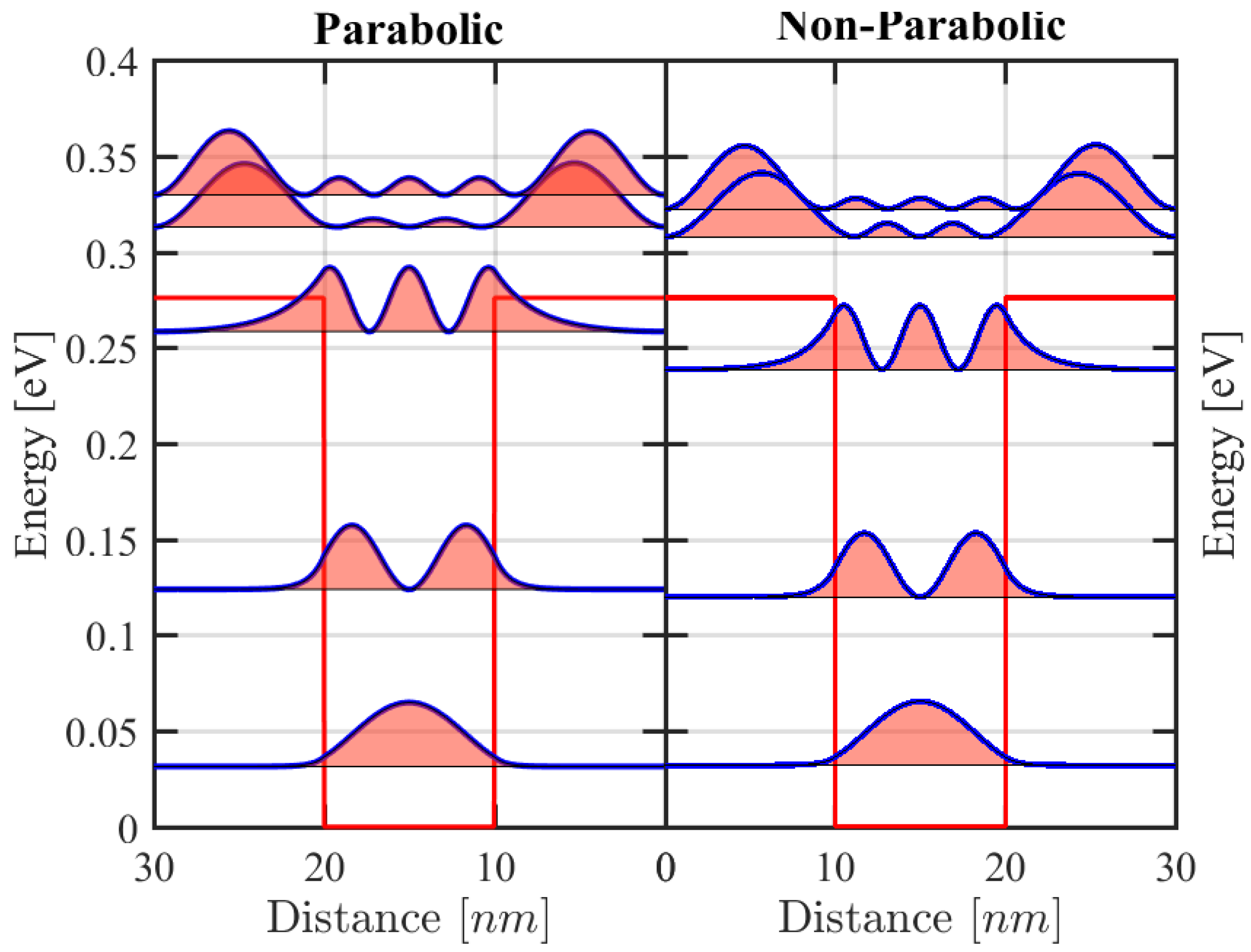
In this section, three applications are shown. First, a case study was solved to validate the accuracy of the simulations to published results using an energy-dependent effective mass non-parabolic model on a structure of a single quantum well [28]. This is a 100 Å GaAs thin well layer surrounded by AlGaAs barrier layers. The barrier height was set to 0.276 eV and the effective masses of electrons at the band edges were taken to be m w / m 0 = 0.067 in the well and m b / m 0 = 0.09 in the barrier. Here, the subscripts w and b denote the well and barrier, respectively, and m 0 is the electron free mass. The in-plane wavevector components k x and k y were set to zero for the purpose of comparison. Using this model, Equations (6) and (7) under the EFA were solved repeatedly by updating the effective masses and eigen energies until their convergence. The results of the second-order Lagrange finite element method are shown in Table 1 along with the results of two other numerical methods, namely the Finite Difference Method (FDM) [32] and the Transfer Matrix Method (TMM) [33], which are also included in the simulation tools developed.
The calculation was carried for both the parabolic and non-parabolic case and the results are compared with Samir et al. [28]. Table 1 lists the confined eigen energies in quantum wells of different widths ranging from 5 Å to 200 Å. The results are in excellent agreement with the reported data. The results also clearly show that the single-band parabolic model leads to energies slightly over estimated for higher lying states. Therefore, our results confirm the effects of including non-parabolicity, which shrinks the confined energy gaps with a noticeable shift in the higher energies.
An illustrative example for such effect is given in Figure 1, where the probability density of the first five states of a 100 Å GaAs quantum well embedded in AlGaAs is shown for the parabolic and non-parabolic case. In both panels, the energies E n are indicated by the thin horizontal lines, and the probability densities | φ ( z ) | 2 by the shaded colored areas. There are only three confined states for electrons. The tunneling of the eigenfunctions through the barriers is larger for states with high energies and decreases from the parabolic to non-parabolic.
The second application that is investigated in this work deals with the calculation of the bulk band structure of InAs material strained by a GaAs substrate of 5.6533 Å lattice constant. Due to the lattice mismatch between these two material, the grown bulk layer experiences an intrinsic compressive strain of −7.09%. The value of strain used in this case is calculated using the formula ( a s u b a ) / a × 100 % where a s u b and a are the lattice constant of the substrate and of InAs material. The overall conduction band and valence bands dispersion using the 8 × 8 k · p Hamiltonian in Equation (1) is obtained by diagonalizing Equation (1) or equivalently by solving the following secular equation at each wavevector k k x , k y , k z :
d e t H α β 8 × 8 ( k ) δ α β E ( k ) = 0 .
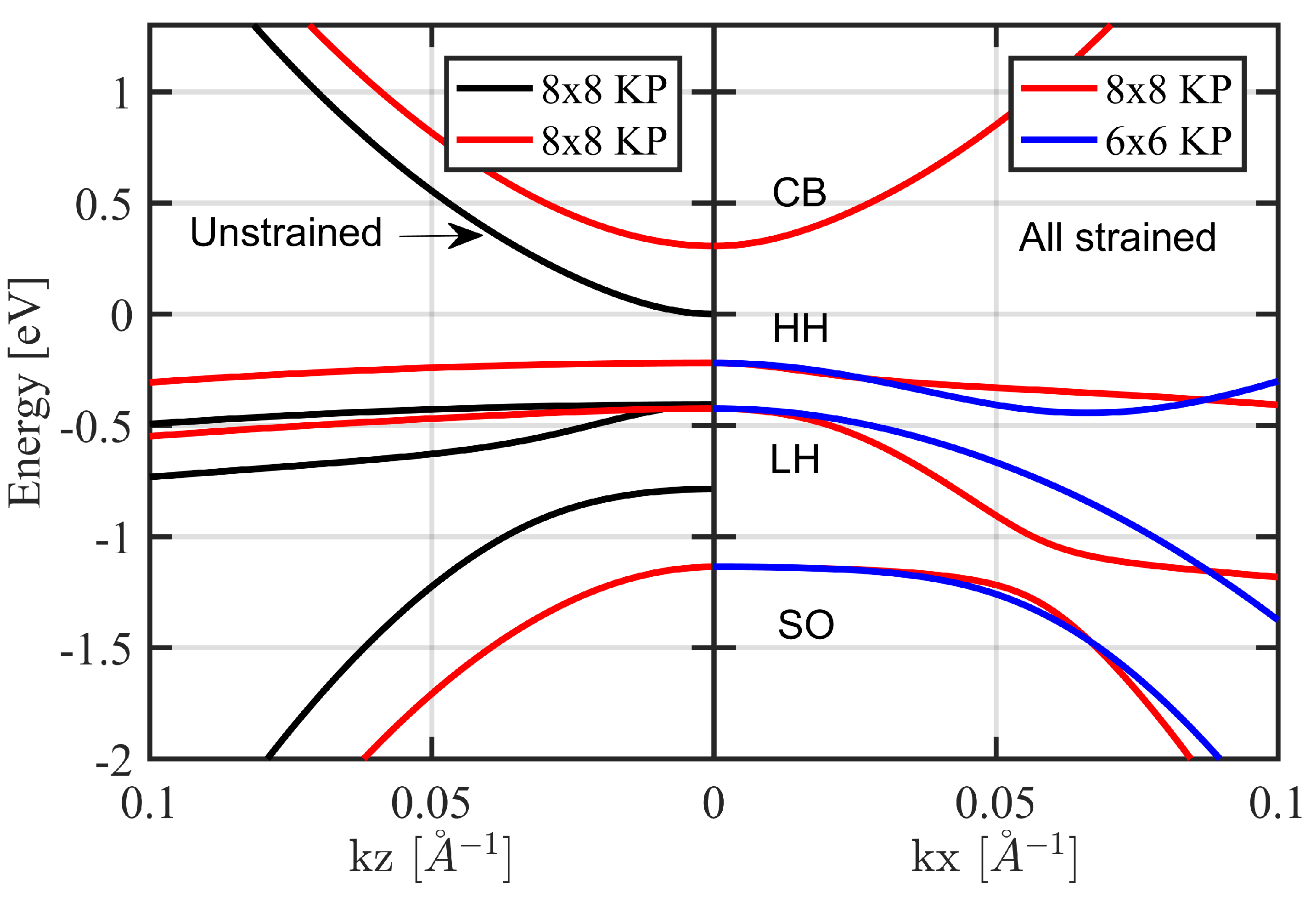
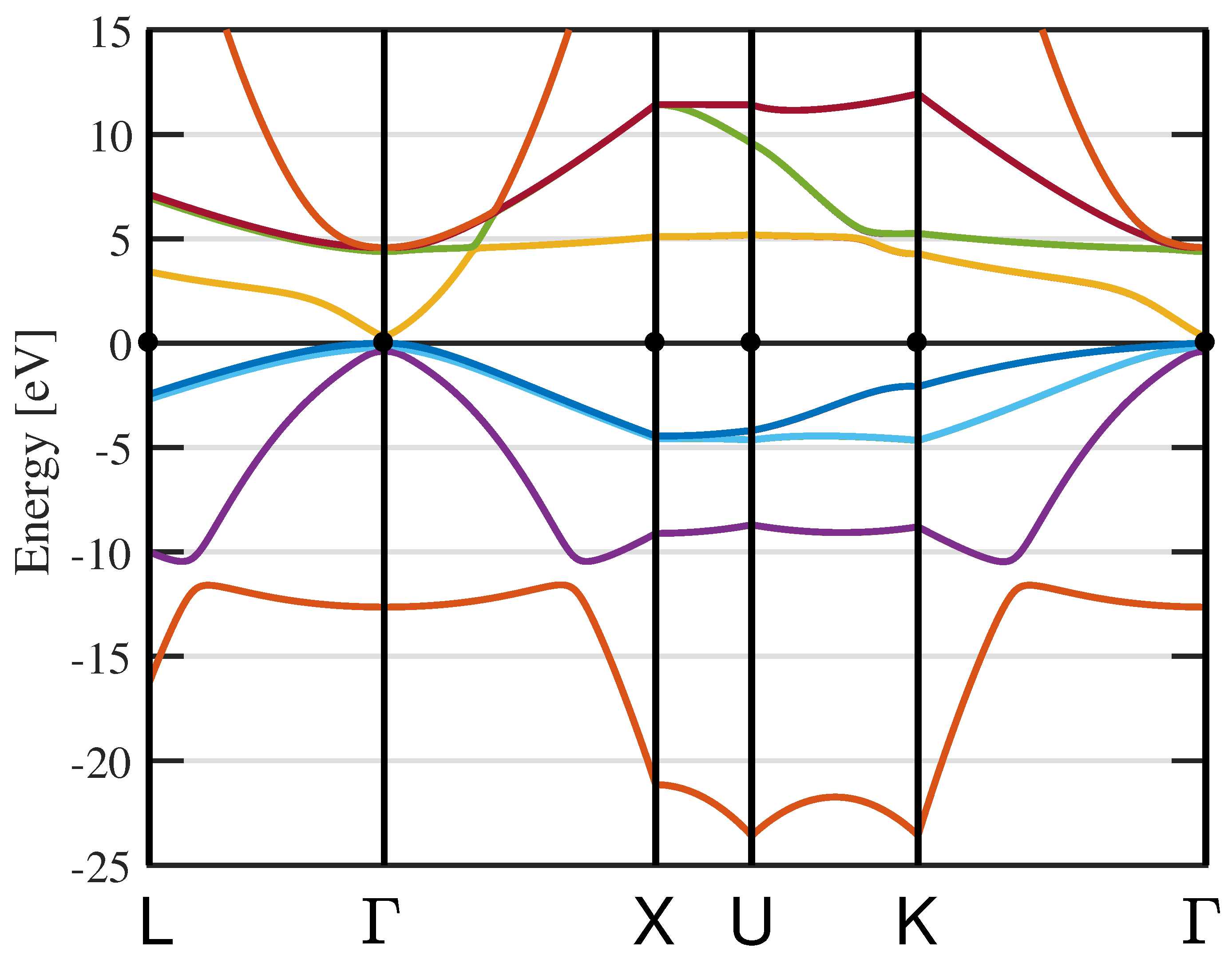
In Figure 2, the overall band structure curves of strained bulk InAs and unstrained standalone bulk InAs are shown along the k x and k z directions, respectively. These curves are dispersions for the conduction band (CB), Heavy Hole (HH), Light Hole (LH), and spin–orbit split-off (SO) valance bands. In Figure 2 (right), the 6 × 6 k · p Hamiltonian curves are shown. This 6 × 6 Hamiltonian couples only the three valance bands and ignores the coupling with conduction band, which is justified only in wide energy gap materials. Within this 6 × 6 Hamiltonian, the conduction-band states, which are not shown in this figure, can be treated separately using single-band model. In narrow energy gap materials such as InAs, the 6 × 6 Hamiltonian results show a discrepancy for higher in-plane wave vectors. Figure 3 shows the band structures of unstrained bulk InA along crystallographic directions pointing to high symmetry points. The Hamiltonian used is the 14 × 14 one from [34], which extends the interaction to more higher bands. The results confirm that including the conduction band into the Hamiltonian increases the conduction band for higher k x values while pushing down LH and SO bands. This effect is negligible on HH band. In Figure 3 (left), the conduction band is parabolic in both directions k x and k z while the valence bands exhibit a non-parabolicity due to mixing effects. The strain lifts the HH and LH bands degeneracy at the zone center. The parabolic isotropy is in fact a reflection of the s-like character of conduction-band states in a bulk semiconductor. Table 2 lists the k · p band parameters used for the calculation [7,35]. It should be noted that the k · p method results are sensitive to the input parameters.
Moreover, the k · p solutions are subject to a well-known problem of unphysical “spurious” solutions, especially with Hamiltonians that include more remote bands or when band parameters have large difference across layers’ interfaces [31].
Such unphysical solutions should be identified and removed from the region of interest. The spurious solutions arise from the incompleteness of the basis states used for the construction of the Hamiltonian [37]. This is still a standing problem; different approaches and models have been proposed to eliminate them but each approach has its drawbacks. Such solutions may appear as highly oscillatory or strongly localized wave functions within the band gap or dispersion curves bending in the wrong direction [38,39,40]. Three main reasons have been identified for the source of the spurious solutions. First, the input experimental parameters can trigger wing-band solutions within the band gap originating from second-order Hamiltonian’s terms at large-k values [38,40,41]. These solutions can be avoided by parameter rescaling procedures [42,43]. Second, the interface between two materials can be subject to localized spurious solutions due to improper boundary condition for the envelope function components. These solutions can be removed by a proper ordering of differential operators [43,44]. Finally, the spurious solutions may also be triggered by the chosen discretization scheme and the mesh width, and it was found to be related to the ill-representation of the first-order derivative terms of the Hamiltonian [40,45].
In the developed simulation tools, two elimination models are implemented. The first one is based on adding a small correction to the off-diagonal elements of the Hamiltonian [41] to discard terms responsible for the spurious solutions and the second one modifies Kane’s parameter P c v [37,38].
Finally, the last test case illustrates the ability of the tools to model a realistic optoelectronic device where the miniband dispersions of the active region of an infrared photodetectors based on type-II InAs/GaSb superlattices are calculated. The studied superlattice is mainly composed of nine InAs/GaSb periods with thicknesses around 44 Å/21 Å, respectively. The InAs layers are chosen to be thicker than GaSb layers to efficiently reduce the dark current [46]. This superlattice is designed to operate in a long wavelength infrared radiation (LWIR) 8–14 μm atmospheric detection window. The potential profile V ( r ) of this active region is periodic and this periodicity is handled using the Bloch theorem, which greatly simplifies the computational task. Within this theorem, the wave function in two adjacent superlattice periods differs only by a phase shift: φ ( z ) = φ ( z p ) e i k p · p where k p is the Bloch wavenumber and p is the superlattice period. From a computational point of view, this boundary condition is implemented by overlaying the last element matrix onto the first one modulated by the factors e ± i k p · p in the global matrix system. The Dirichlet boundary condition is implemented by setting the envelope function to zero at the external borders of the structure. Type II InAs/GaSb superlattice is made of narrow energy gap materials in which the coupling between conduction bands and valance bands is strong; therefore, the 8 × 8 k · p Hamiltonian in Equation (1) should be used. To account for this strong interaction, the original electron effective mass m e * in the diagonal Hamiltonian matrix as well as the original Luttinger parameters γ 1 , γ 2 , and γ 3 should be updated according to:
m 0 m e * = m 0 m c * E p E g + 2 Δ / 3 E g E g + Δ
γ 1 = γ 1 L E p 3 E g + Δ γ 2 = γ 2 L 1 2 E p 3 E g + Δ γ 3 = γ 3 L 1 2 E p 3 E g + Δ
where m c * , γ 1 L , γ 2 L , and γ 3 L are now the original effective mass and the original Luttinger parameters, respectively. These normalizations are only required with Hamiltonians of size greater than 8 × 8. This is because the strong interaction is explicitly included in the formulation of the eight-band model, whereas, in smaller size k · p models, the valence and conduction bands are decoupled and the Luttinger parameters are adjusted using Löwdin perturbation method [47]. Using the Löwdin perturbation, method, the Hamiltonian is reduced to a smaller number of relevant bands, including the effect of the remote bands perturbatively. In all calculations, the symmetrization rules given by Equation (12) are applied to taken into account the real space dependence of the bulk band parameters.
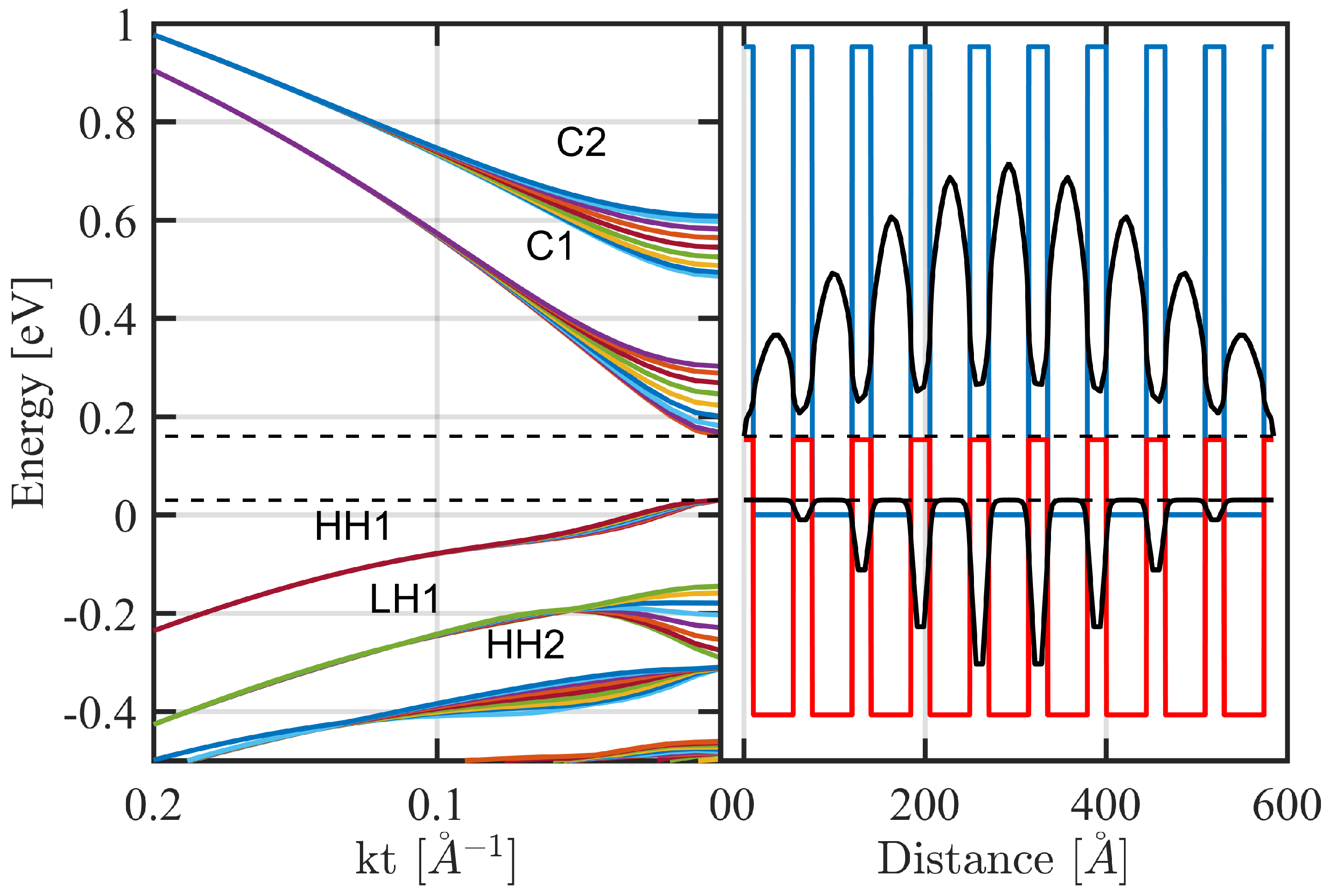
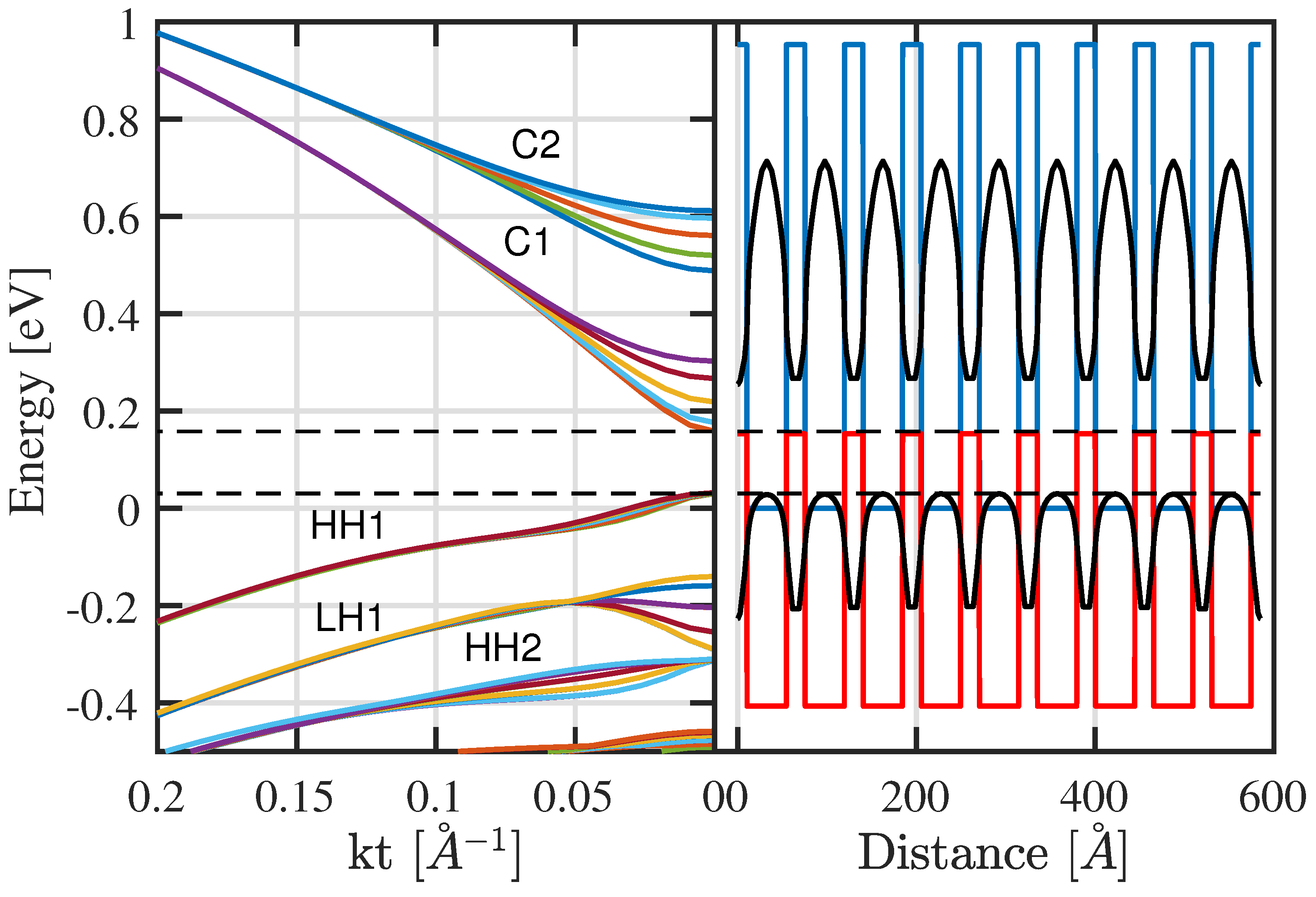
The band edge profile potential emanating from a structure of a nine-period InAs/GaSb44 Å/21 Å superlattice, simulated using our model is shown in Figure 4 (right). The corresponding miniband energy-dispersions versus in-plane wavevector k t solved using Dirichlet boundary conditions are shown in Figure 4 (left). In this figure, the reference of energy is taken to be the unstrained conduction band edge of InAs layers with a VBO value of 560 meV. The formation of minibands confirms the quantum mechanical intuition that, since electrons and holes in InAs/GaSb Type II superlattice are separated in space, confined electrons in thin InAs layers form their mini-bands due to overlap of electron wave functions. Similarly, the interaction among holes in thin GaSb layers leads to hole minibands.
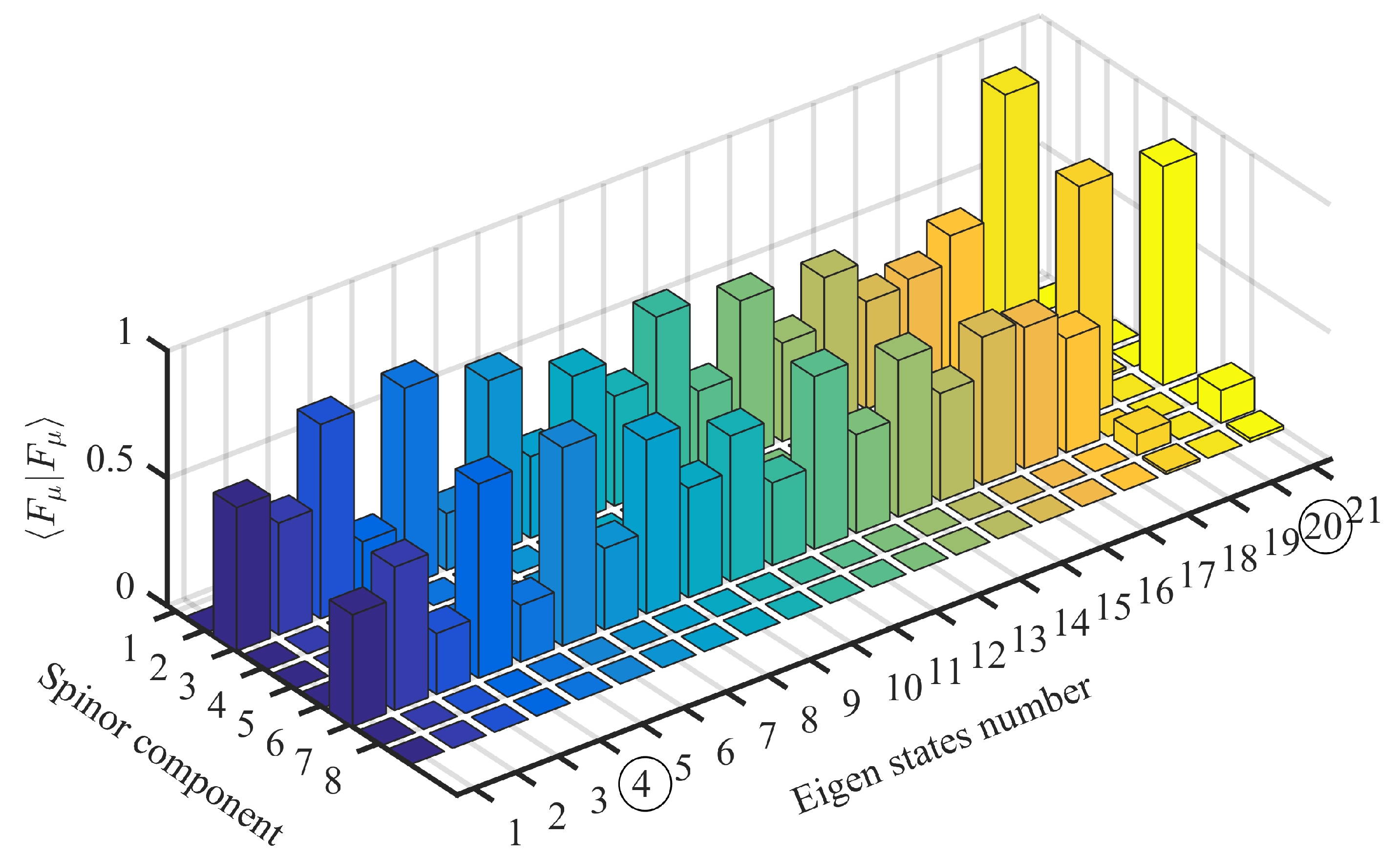
The Hamiltonian used is the full 8 × 8 k · p model without block diagonalization. The fundamental electron and heavy-hole envelope-function component moduli squared for nine periods solved using Dirichlet boundary conditions are shown in Figure 4 (right). At k t = 0 , a classification of minibands states as heavy-hole, light-hole, and split-off states is possible, and are denoted by HHn, LHn, and SOn (n is the quantum number of the subband), respectively. The minibands nomination are assigned based on the dominance of envelope functions at the band edges [7], although this is usually not achievable with the eight band model and with all other higher multi-band k · p models exhibiting strong band mixing. The case is worse with narrow gap systems such as InAs/GaSb and type II heterostructures with a broken gap. The distribution of the eight components of the envelope function spinor F μ | F μ for the 21 eigenstates solution of Equation (19) near the effective gap is plotted in Figure 5. In this figure, the states numbered 4 and 20 have the largest components F μ | F μ among all other states. In addition, State 20 has the largest component F 1 | F 1 corresponding to S | S , indicating a s-like character of conduction-band, while State 4 is mostly dominated by the two largest components F 2 | F 2 and F 6 | F 6 , indicating a mixture of valence band character. Therefore, these two states correspond, respectively, to the lowest state of a conduction miniband C1 and a highest state of a valence miniband HH1. The band dispersion of the SOn states are of less practical interest due to their lower energy range compared to the range of HHn and LHn states and therefore are not shown.
The energy dispersion relations and the corresponding fundamental electron and heavy-hole envelope-function component moduli squared for a nine-period InAs/GaSb 44 Å/21 Å grown on GaSb substrate solved using Periodic boundary conditions are illustrated in Figure 6. Since there are nine degenerate set of subbands under Dirichlet boundary conditions, each of which belongs to one period, the strong interaction lifts the degeneracy into nine states for each subband, as shown in Figure 4. In general, each state splits into N p states where N p is the number of periods. Using periodic boundary conditions, because of the double degeneracy of ± k p states, E ( + k p ) = E ( k p ) , the degeneracy is lifted only into five states for each subband, as shown in Figure 6. For both cases of boundary conditions, the dispersion relations converge at higher in-plane wavevector k t as the interaction becomes weaker. The time for the entire calculation in this case study using coarse meshing is 608.18 s. Obviously, the higher is the complexity of design, the longer is the execution time. This time increases with the increase in the number of layers, the size of the Hamiltonian, and the number of in-plane wave vector sampling points. However, it could be optimized with the FEM approach where, for larger layers, one can use coarse mesh instead of fine mesh for thin layers. In fact, it could be further optimized by using Hermit shape functions.
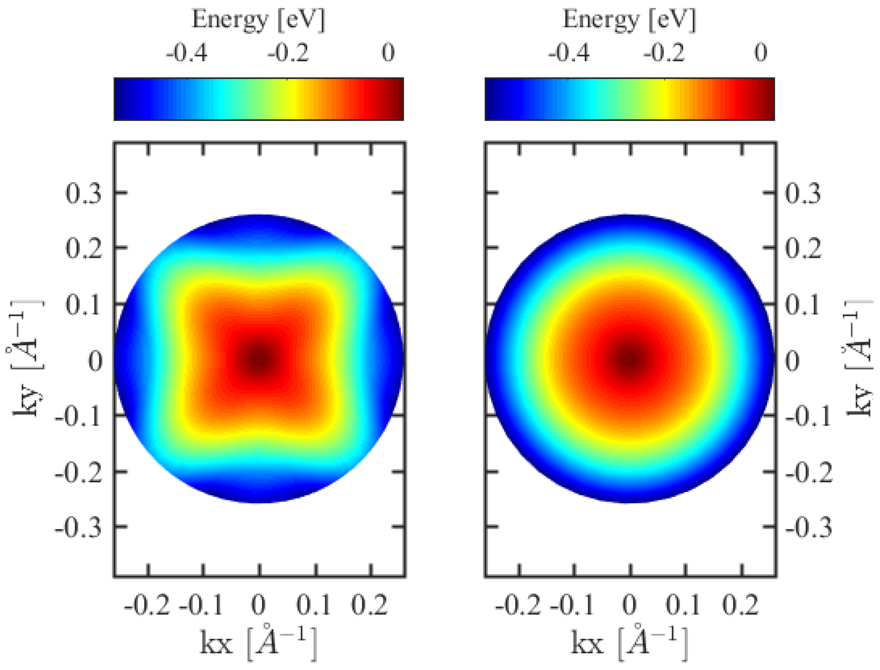
The full form of the 8 × 8 Hamiltonian used in this work is reflected in the anisotropy of band structure. Figure 7 shows the fundamental heavy hole sub-band structure in polar coordinates for both full and block diagonalized Hamiltonian. The anisotropy is strong in the transversal [110] direction for the full form and is absent in the block diagonalized one, which yields unrealistic isotropic in-plane masses in the later case. This anisotropy is usually neglected in previous works where the axial approximation is usually used after block-diagonalization. The transversal directions along which the dispersion relations exhibit the largest difference are [100] and [110]. This anisotropy of the sub-band is estimated by the difference E [ 100 ] ( k t ) E [ 110 ] ( k t ) . Between ( k x = 1 , k y = 0 ) 1 ) and ( k x = 1 , k y = 1 ) 1 ), it was found to be about −90 meV, which indicates that the effective mass is slightly larger along the [110] direction than the [100] direction. This observation confirms that the hole sub-bands are neither parabolic nor isotropic, as can be seen from the dispersion curves.
Despite the difference between the two types of boundary conditions used, the effective band gaps and band edges at the zone center are expected to be comparable since there is no phase shift between the envelope functions at k p = 0 . As indicated in Figure 4 and Figure 6, the effective bandgap is determined by the difference between the bottom of the lowest electron miniband (C1) and the top of the highest hole miniband (HH1) and it has the value of 0.13 eV, which is in excellent agreement with the one experimentally reported by [48] and theoretically with the absorption spectrum reported in Figure 8. This effective gap can be tuned by changing the layer thickness and is primarily determined by the position of the C1 bottom edge since the HH1 band width is less sensitive to layer thickness [49]. The HH1 band width is too small which might be interpreted as it experiences a balanced effect between higher and lower bands. The absorption spectrum at photon energy w is derived from Fermi’s golden rule as:
α w = 4 π 2 e 2 n r c ε 0 m 0 2 w L S n , m k t | Ψ n k t | e ^ · P | Ψ m k t | 2 × f c n ( k t ) f v m ( k t ) × L ( k t , w )
where ε 0 and C are the speed of light and permittivity in a vacuum, and n r and L are the refractive index and the thickness of the superlattice, respectively. f c n and f v m are the Fermi functions for the mth valence sub-band with an energy E v m and the nth conduction sub-band with an energy E c n , respectively, given by:
f c n ( k t ) = 1 1 + e x p E c n ( k t ) F n K B T
f v m ( k t ) = 1 1 + e x p E v m ( k t ) F m K B T
To account for different scattering relaxations causing finite transition linewidth, a normalized Gaussian or Lorentzian L ( k t , w ) distribution function with a broadening γ parameter can be chosen. The summation over k t takes into account the spin degeneracy. The calculation of the optical transition matrix elements Ψ n k t | e ^ · P | Ψ m k t between the hole sub-bands and the electron subbands for TE ( e z ^ )- or TM ( e z ^ )-polarized optical beams requires the evaluation of a dense 8 × 8 momentum matrix P:
P 8 × 8 = m 0 k H
Then, the final expression for the momentum matrix elements reads:
Ψ n k t | e ^ · P | Ψ m k t = e ^ · μ , μ F μ n * ( k t , z ) m 0 k H μ , μ F μ m ( k t , z ) d z
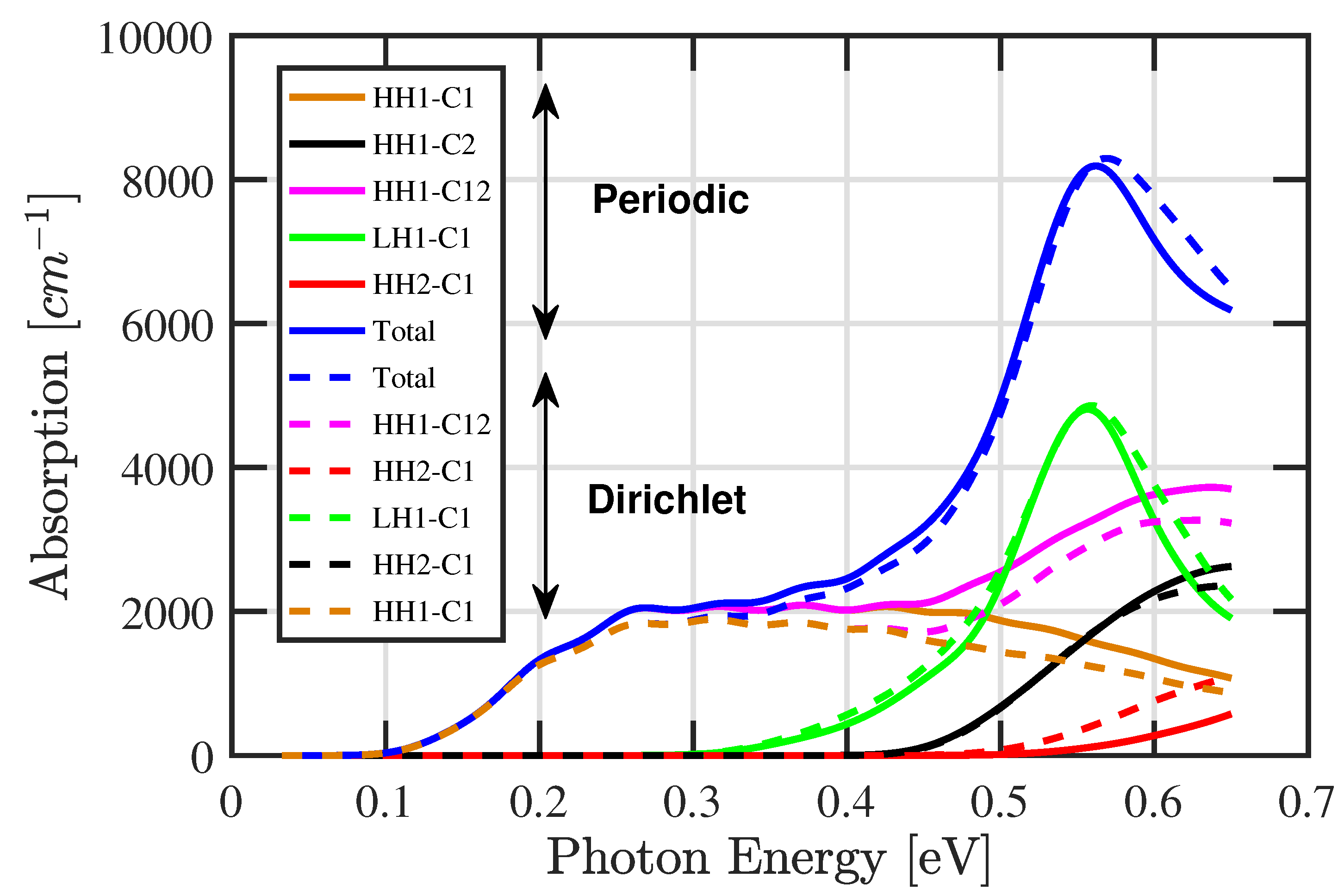
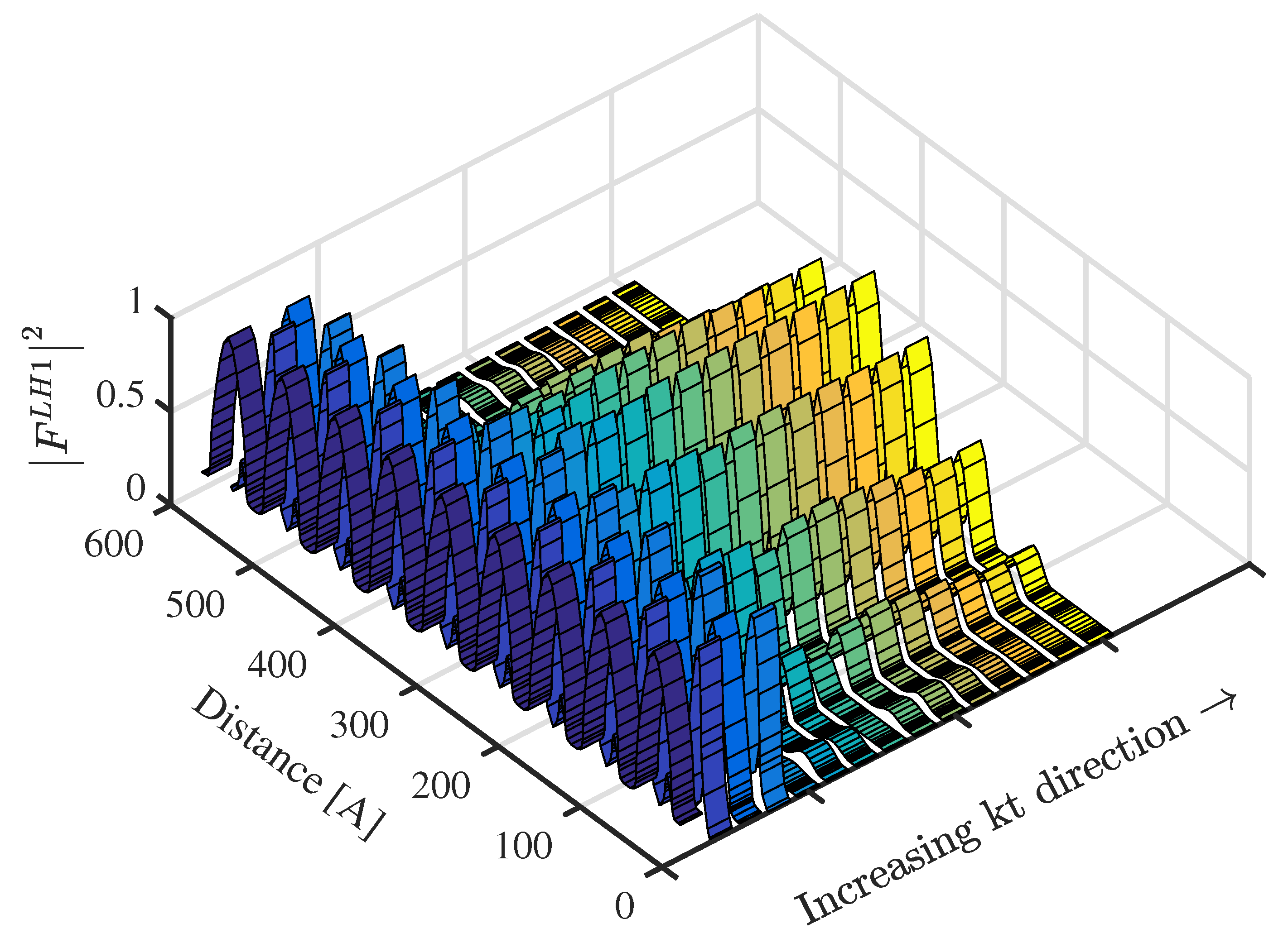
To accelerate the evaluation of these elements, the derivatives of the Hamiltonian elements are calculated explicitly in terms of spinor envelope components and are given in Appendix A. Using Equations (A1) and (A2), the average time required to calculate the matrix element of a single transition at a given in-plane wavevector is reduced from 7 s to 0.7 s compared to the direct Hamiltonian derivation method. Figure 8 shows the total absorption spectrum for nine-period InAs/GaSb 44 Å/21 Å type II superlattice using both kind of boundary conditions. The cutoff energies for different types of interband transitions are consistent with the effective band gaps between different sub-bands predicted in Figure 4 and Figure 6. The maxima observed in Figure 8 of around 550 meV indicate a large wavefunction overlap of around this energy value due to larger in-plane wavevector states’ contributions, where the hole dispersions are neither parabolic nor isotropic. Figure 9 shows the largest envelope function spinor component dependent on in-plane wavevectors near the LH1 miniband. Clearly, the in-plane states’ contributions are high to produce the absorption maxima.
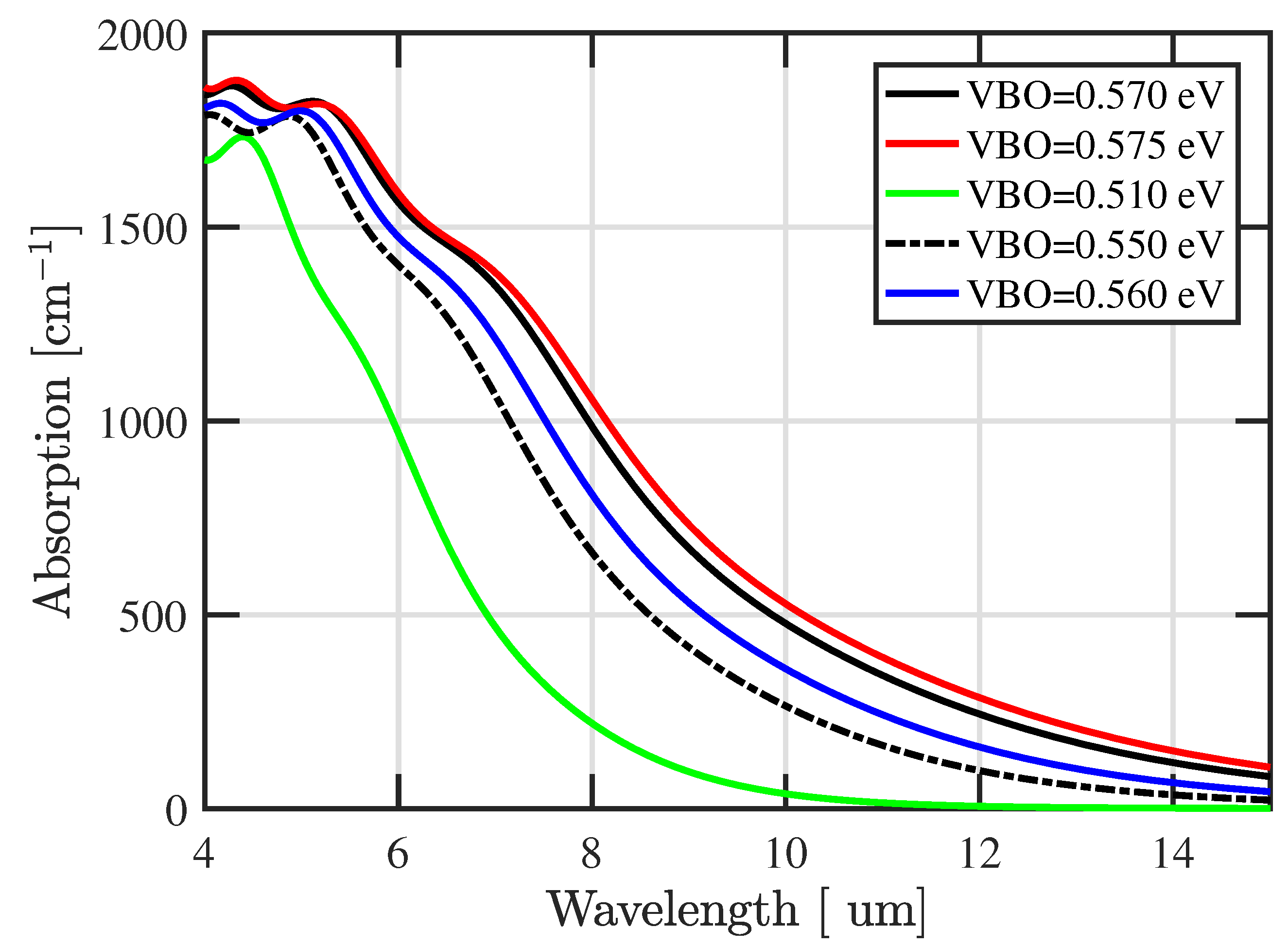
To clarify the sensitivity to the input parameters in Figure 10, the absorption spectrum for different valence band offset (VBO) values is calculated. As could be inferred from Figure 10, an increase of InAs/GaSb superlattice’s VBO from 510 meV to 575 meV leads to an increase of the absorption coefficient. Such a sensitivity indicates that the type II superlattice structure should be properly designed to achieve maximum quantum efficiency in real devices such as infrared detectors. In addition, for the LWIR window, a shift of nearly 1 μm in the cutoff wavelength is due to 5 meV change in the VBO. Our calculations show that the LWIR cutoff wavelength is in a good agreement with the experimental data from reference [48].
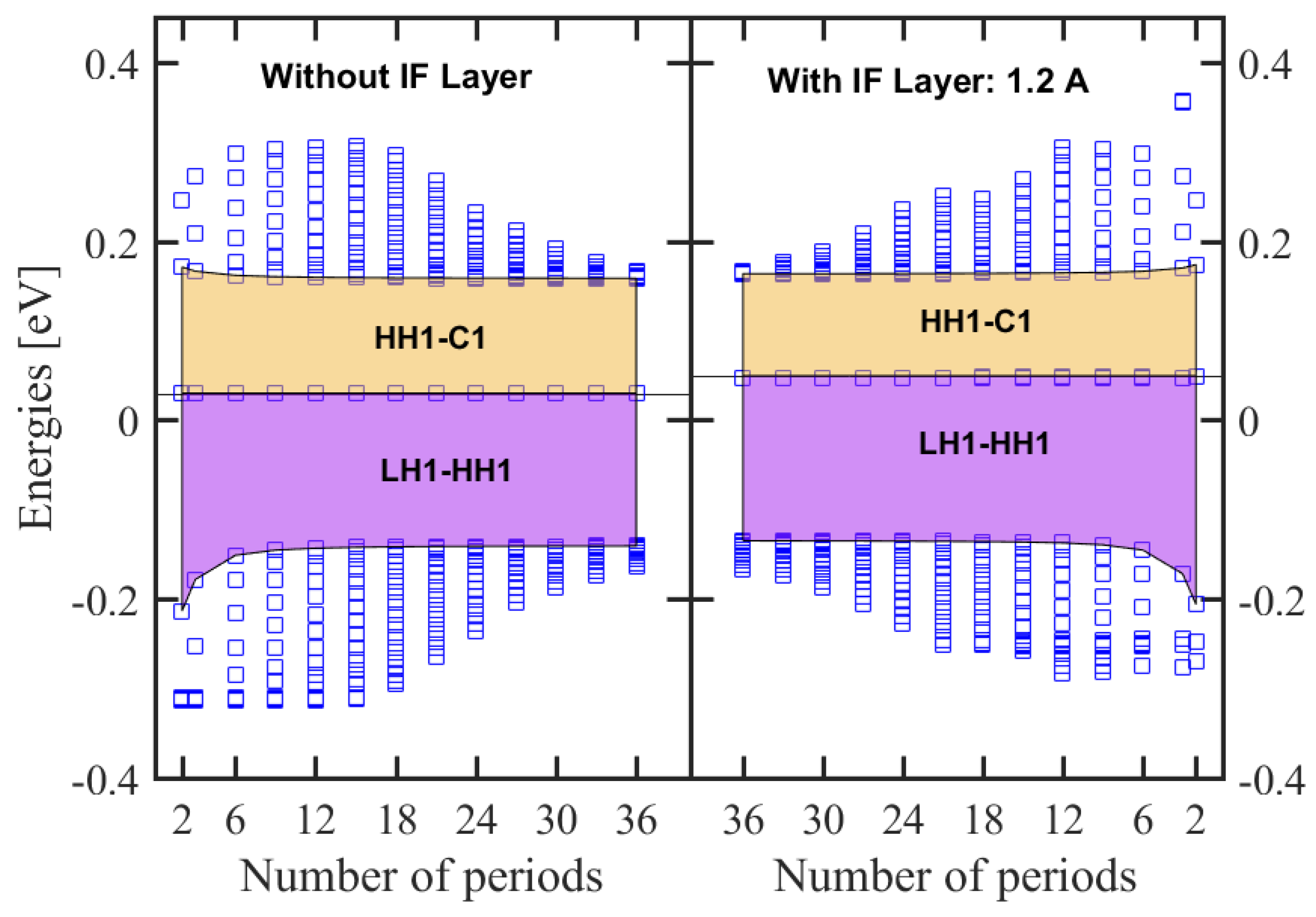
There exists a further complication with InAs/GaSb superlattices. Although the separation of the confined states and minibands can be tuned to a desired IR windows by adjusting the InAs and GaSb layer thicknesses, it was found that the physical and optical properties and device performance depend critically on the composition and structure of interfaces formed at the heterojunctions. Recent studies demonstrated that the interface InAs/GaSb is not always abrupt and in fact has chemical asymmetries in compositional profile due to segregation of Sb and In atoms at the interfaces [50,51]. This segregation leads to the formation of unintentional interfaces (IFs) with different composition configurations. For InAs/GaSb SLs, IFs often turn out to be InSb-like or GaAs-like. Previous studies modeled IF’s effect either by fine-tuning the VBO values or the use of an interface potential profile (short-range delta function potentials centered at the interface [52] and graded or asymmetric interface [53,54]). However, these approaches miss the effect of the intrinsic strained property of IFs on the electronic structure and the optical properties. The most successful approach is to insert InSb layers to account for large IFs lattice mismatch and the strain effect. A structure with an IF layer is obtained by introducing an interface InSb layer between InAs and GaSb on both sides, while the thickness of one superlattice period is kept fixed. The change in the fundamental effective gap as a function of the number of periods N are plotted in Figure 11 for InAs/GaSb 44 Å/21 Å SL without and with InSb IF layer forced at 1.2 Å.
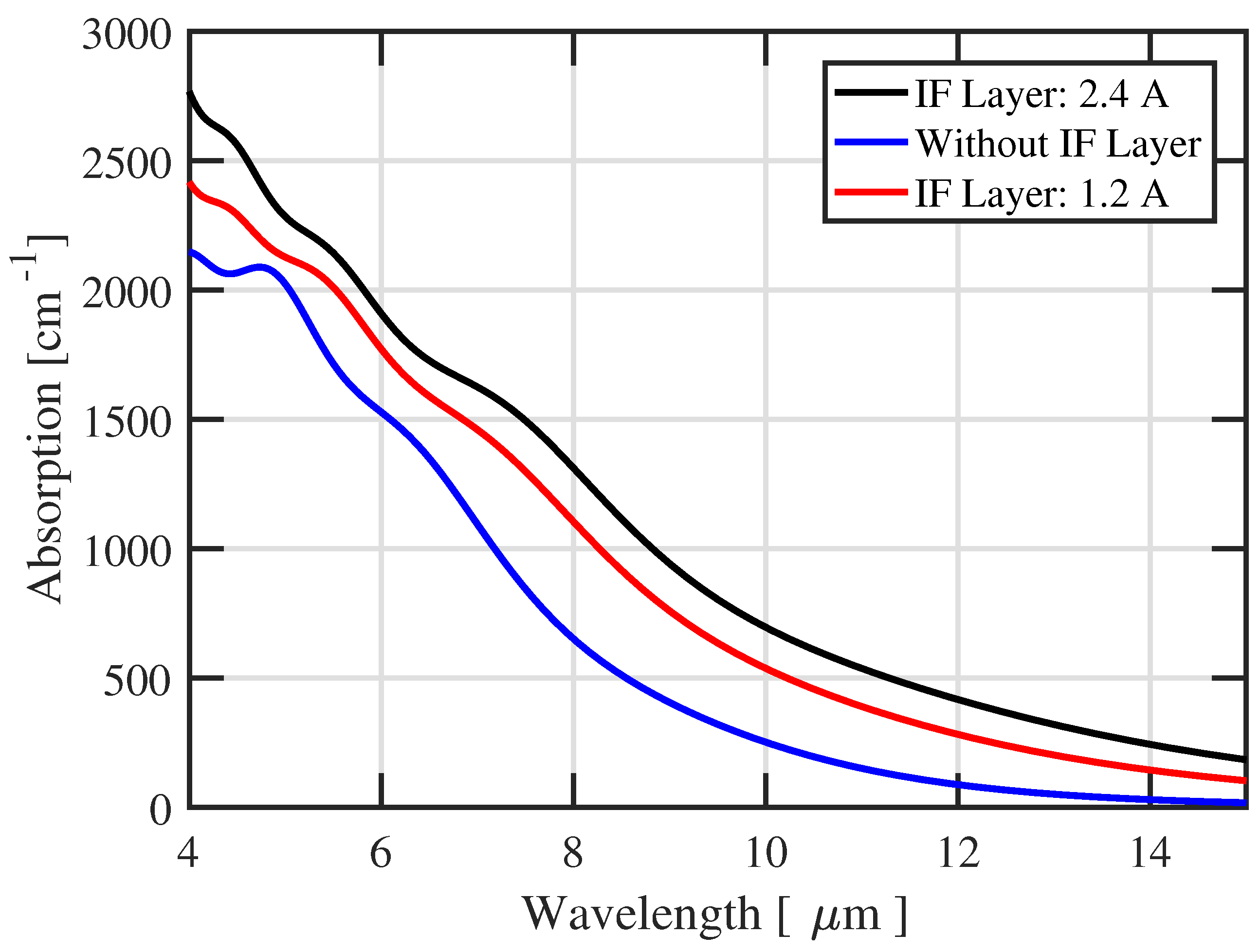
For small number of periods, the effective gap exhibits a strong variation, which indicates the quantum mechanical interaction and the start of miniband formation, while, for a higher number of periods, the effective gap tends to converge to the fundamental minibands gap of the superlattice. For very small periods, the large scatter of eigen energies is a signature of the single quantum well confinement. The presence of InSb IF layer induces a decrease in the effective energy about 25%. This is because the valence band state energies are shifted upward due to the presence of hole states in InSb layer lying in a higher level than those in InAs and GaSb, whereas this effect is negligible with conduction band states since these states in InSb are in between the corresponding ones in InAs and GaSb. The overall effect of including IF layers on the HH miniband is minor with an upward shift less than 6 meV. The absorption coefficients with effect of interfacial layers taken into account are shown in Figure 12 indicating an increasing shift in the cut-off wavelengths with IF layers thickness.
5. Conclusions

In this work, an efficient, accurate and rigorous model for the overall band structure calculation based on the k · p approach is presented and tested for cubic zincblende bulk semiconductor materials as well as for their heterostructures. These modeling tools are useful for the design of optoelectronic devices and the estimation of their performance. The tools include different k · p Hamiltonian formulations namely: 14 × 14, 8 × 8, 6 × 6, 4 × 4, and single band non-parabolic model. These models take into account the strain effects and can be invoked easily within the modeling steps. The results of the using a non-parabolic model are in excellent agreement with published data. The predicted cutoff energies for different types of interband transitions are consistent with the calculated band dispersion curves of InAs/GaSb Type II broken gap superlattice and demonstrate excellent agreement with the experimental data reported in [48]. Our modeling shows that the IF’s lattice mismatch and induced strain yields a significant increase in the absorption coefficient as well as in cut-off wavelengths. As a result, a wide tunable range of optical properties can be obtained with IF layers. Finally, the model can be extended easily to cover materials belonging to wurtzite crystal symmetry just by generating the correct Hamiltonian.

Author Contributions

Z.B. and A.B. were mainly responsible for writing the original draft, developing and validating the model and analysing the important information presented in the manuscript. N.S. contributed to the funding acquisition and project administration.

Acknowledgments

The authors acknowledge the financial support of the Ministry of Higher Education and Scientific Research, Algeria. The authors are also grateful to the valuable discussion with Phil Picton that contributed to enriching the final version of the manuscript.

Conflicts of Interest

The authors declare no conflict of interest.

Appendix A. Momentum Matrix Elements

We provide here the explicit derivation of matrix elements n P m = Ψ n k t | ( x ^ + y ^ ) · P | Ψ m k t corresponding to TE transition mode between the initial spinor | Ψ m k t and the final spinor | Ψ n k t . These are for the 8 × 8 KP Hamiltonian given by Equation (1) and are evaluated for any direction in transversal reciprocal k t ( k x , k y ) space and in terms of spinor envelope components | S m k t from the initial vector state and | F n k t from the final vector state. In the following, the subscript k t has been dropped for convenience.
n P m x = d z F 1 * m 0 m e * k x S 1 + P c v m 0 6 3 S 2 + S 7 + 2 S 8 + F 2 * i P c v m 0 2 S 1 k x γ 1 + γ 2 S 2 + 3 γ 2 k x i γ 3 k y S 7 + 2 S 8 i 3 2 γ 3 z S 3 + z S 4 + F 3 * P c v m 0 6 S 5 k x γ 1 γ 2 S 3 + 2 γ 2 k x S 4 + 3 γ 2 k x i γ 3 k y S 6 + i 3 2 γ 3 z S 2 + 3 2 z S 8 + F 4 * P c v m 0 3 S 5 + k x 2 γ 2 S 3 γ 1 S 4 6 γ 2 k x i γ 3 k y S 6 + i 3 2 2 γ 3 z S 2 + 3 z S 7 + F 5 * m e * k x S 5 + P c v m 0 6 S 3 + 2 S 4 + 3 S 6 + F 6 * + P c v m 0 2 S 5 k x γ 1 + γ 2 S 6 3 γ 2 k x + i γ 3 k y S 3 + 2 S 4 i 3 2 γ 3 z S 7 + 1 2 z S 8 + F 7 * P c v m 0 6 S 1 k x γ 1 γ 2 S 7 + 3 γ 2 k x + i γ 3 k y S 2 2 γ 2 k x S 8 i 3 2 γ 3 3 2 z S 4 z S 6 + F 8 * P c v m 0 2 S 1 2 γ 2 k x S 7 γ 1 k x S 8 + 6 γ 2 k x + i γ 3 k y S 2 i 3 2 γ 3 3 2 z S 3 + 1 2 z S 6 + i 3 γ 3 2 S 3 + 1 2 S 4 z F 2 * S 2 + 3 2 S 8 z F 3 * 3 2 S 7 + 1 2 S 2 z F 4 * + S 7 1 2 S 8 z F 6 * + 3 2 S 4 S 6 z F 7 * + 3 2 S 3 1 2 S 6 z F 8 * .
n P m y = d z F 1 * m 0 m e * k y S 1 i P c v m 0 6 3 S 2 + S 7 + 2 S 8 + F 2 * i P c v m 0 2 S 1 h b k y γ 1 + γ 2 S 2 3 γ 2 k y + i γ 3 k x S 7 + 2 S 8 3 2 γ 3 z S 3 + 1 2 z S 4 + F 3 * i P c v m 0 6 S 5 3 γ 2 k y + i γ 3 k x S 6 k y γ 1 γ 2 S 3 + 2 γ 2 k y S 4 3 2 γ 3 z S 2 3 2 z S 8 + F 4 * i P c v m 0 3 S 5 + k y 2 γ 2 S 3 γ 1 S 4 + 6 γ 2 k y + i γ 3 k x S 6 + 3 2 2 γ 3 z S 2 + 3 z S 7 + F 5 * m 0 m e * k y S 5 i P c v m 0 6 S 3 2 S 4 + 3 S 6 + F 6 * i P c v m 0 2 S 5 k y γ 1 + γ 2 S 6 + 3 γ 2 k y + i γ 3 k x S 3 2 S 4 + 3 2 γ 3 z S 7 1 2 z S 8 + F 7 * i P c v m 0 6 S 1 + 3 γ 2 k y + i γ 3 k x S 2 k y γ 1 γ 2 S 7 2 γ 2 k y S 8 + 3 2 γ 3 3 2 z S 4 + z S 6 + F 8 * i P c v m 0 3 S 1 2 γ 2 k y S 7 γ 1 k y S 8 + 6 γ 2 k y + i γ 3 k x S 2 + 3 2 γ 3 3 2 z S 3 1 2 z S 6 + 3 γ 3 2 S 3 + 1 2 S 4 z F 2 * S 2 3 2 S 8 z F 3 * + 3 2 S 7 1 2 S 2 z F 4 * + S 7 1 2 S 8 z F 6 * + 3 2 S 4 + S 6 z F 7 * + 3 2 S 3 1 2 S 6 z F 8 * .

References

  1. Agarwal, S.; Balamukundhan, K.; Neophytou, N.; Klimec, G. 1D hetero-structure tool for atomistic simulation of nano-devices. In Proceedings of the TECHCON, Austin, TX, USA, 15 September 2008. [Google Scholar]
  2. Ting, D.Z.; Soibel, A.; Khoshakhlagh, A.; Höglund, L.; Keo, S.A.; Rafol, S.B.; Hill, C.J.; Fisher, A.M.; Luong, E.M.; Nguyen, J.; et al. Antimonide Type-II Superlattice Barrier Infrared Detectors; Andresen, B.F., Fulop, G.F., Hanson, C.M., Miller, J.L., Norton, P.R., Eds.; International Society for Optics and Photonics: Bellingham, WA, USA, 2017; p. 101770N. [Google Scholar]
  3. Maimon, S.; Wicks, G.W. nBn detector, an infrared detector with reduced dark current and higher operating temperature. Appl. Phys. Lett. 2006, 89, 151109. [Google Scholar] [CrossRef]
  4. Li, J.V.; Yang, R.Q.; Hill, C.J.; Chuang, S.L. Interband cascade detectors with room temperature photovoltaic operation. Appl. Phys. Lett. 2005, 86, 101102. [Google Scholar] [CrossRef]
  5. Kim, C.S.; Kim, M.; Bewley, W.W.; Lindle, J.R.; Canedy, C.L.; Abell, J.; Vurgaftman, I.; Meyer, J.R. Corrugated-sidewall interband cascade lasers with single-mode midwave-infrared emission at room temperature. Appl. Phys. Lett. 2009, 95, 231103. [Google Scholar] [CrossRef]
  6. Rogalski, A.; Martyniuk, P.; Kopytko, M. InAs/GaSb type-II superlattice infrared detectors: Future prospect. Appl. Phys. Rev. 2017, 4, 31304. [Google Scholar] [CrossRef]
  7. Qiao, P.-F.; Mou, S.; Chuang, S.L. Electronic band structures and optical properties of type-II superlattice photodetectors with interfacial effect. Opt. Express 2012, 20, 2319. [Google Scholar] [CrossRef] [PubMed]
  8. Payne, M.C.; Teter, M.P.; Allan, D.C.; Arias, T.A.; Joannopoulos, J.D. Iterative minimization techniques for ab initio total-energy calculations: molecular dynamics and conjugate gradients. Rev. Mod. Phys. 1992, 64, 1045–1097. [Google Scholar] [CrossRef]
  9. Jacoboni, C.; Lugli, P. The Monte Carlo Method for Semiconductor Device Simulation; Computational Microelectronics; Springer: Vienna, Austria, 1989; ISBN 978-3-7091-7453-1. [Google Scholar]
  10. Yu, P.Y.; Cardona, M. Fundamentals of Semiconductors; Graduate Texts in Physics; Springer: Berlin/Heidelberg, Germany, 2010; ISBN 978-3-642-00709-5. [Google Scholar]
  11. Kelly, M.J. Low-Dimensional Semiconductors: Materials, Physics, Technology, Devices; Clarendon Press: Oxford, UK, 1995; ISBN 9780198517818. [Google Scholar]
  12. Enderlein, R.; Horing, N.J. Fundamentals of Semiconductor Physics and Devices; World Scientific: Singapore, 1997; ISBN 978-981-02-2387-8. [Google Scholar]
  13. Askar, A. Finite element method for bound state calculations in quantum mechanics. J. Chem. Phys. 1975, 62, 732. [Google Scholar] [CrossRef]
  14. Ram-Mohan, L.R.; Saigal, S.; Dossa, D.; Shertzer, J. The finite-element method for energy eigenvalues of quantum mechanical systems. Comput. Phys. 1990, 4, 50. [Google Scholar] [CrossRef]
  15. Guimarães, M.N.; Prudente, F.V. A study of the confined hydrogen atom using the finite element method. J. Phys. B Atomic Mol. Opt. Phys. 2005, 38, 2811–2825. [Google Scholar] [CrossRef]
  16. Nakamura, K.; Shimizu, A.; Koshiba, M.; Hayata, K. Finite-element analysis of quantum wells of arbitrary semiconductors with arbitrary potential profiles. IEEE J. Quantum Electron. 1989, 25, 889–895. [Google Scholar] [CrossRef]
  17. Ram-Mohan, L.R. Finite Element and Boundary Element Applications in Quantum Mechanics; Oxford University Press: Oxford, UK, 2002; ISBN 9780198525219. [Google Scholar]
  18. Ferrari, R.L. Electronic band structure for two-dimensional periodic lattice quantum configurations by the finite element method. Int. J. Numer. Model. Electron. Netw. Devices Fields 1993, 297, 283–297. [Google Scholar] [CrossRef]
  19. Park, S.-H.; Ahn, D.; Lee, Y.-T. Finite element analysis of valence band structures in quantum wires. J. Appl. Phys. 2004, 96, 2055. [Google Scholar] [CrossRef]
  20. Yi, J.C.; Dagli, N. Finite-Element Analysis of Valence Band Structure and Optical Properties of Quantum-Wire Arrays on Vicinal Substrates. IEEE J. Quantum Electron. 1995, 31, 208–218. [Google Scholar]
  21. Luttinger, J.M.; Kohn, W. Motion of Electrons and Holes in Perturbed Periodic Fields. Phys. Rev. 1955, 97, 869–883. [Google Scholar] [CrossRef]
  22. Bir, G.L.; Pikus, G.E. Symmetry and Strain-Induced Effects in Semiconductors; John Wiley: New York, NY, USA, 1974. [Google Scholar]
  23. Kane, E.O. Handbook of Semiconductors; North-Holland: Amsterdam, The Netherlands, 1982; Volume 1, p. 193. [Google Scholar]
  24. Kolokolov, K.I.; Savin, A.M.; Beneslavski, S.D.; Minina, N.Y.; Hansen, O.P. Energy spectrum and topology evolution of the Fermi surface of two-dimensional holes in GaAs/Al0.5 Ga0.5 As heterostructures under uniaxial compression: Theory and experiment. Phys. Rev. B 1999, 59, 7537–7545. [Google Scholar] [CrossRef]
  25. Chang, C.-S.; Chuang, S.L. Modeling of Strained Quantum- Well Lasers with Spin-Orbit Coupling. IEEE J. Sel. Top. Quantum Electron. 1995, 1, 218–229. [Google Scholar] [CrossRef]
  26. Nelson, D.F.; Miller, R.C.; Kleinman, D.A. Band nonparabolicity effects in semiconductor quantum wells. Phys. Rev. B 1976, 35, 7770–7773. [Google Scholar] [CrossRef]
  27. Bastard, G. Superlattice band structure in the envelope-function approximation. Phys. Rev. B 1981, 24, 5693. [Google Scholar] [CrossRef]
  28. Rihani, S.; Page, H.; Beere, H.E. Quasibound states in semiconductor quantum well structures. Superlattices Microstruct. 2010, 47, 288–299. [Google Scholar] [CrossRef]
  29. Ram-Mohan, L.R.; Yoo, K.H.; Aggarwal, R.L. Transfer-matrix algorithm for the calculation of the band structure of semiconductor superlattices. Phys. Rev. B 1988, 38, 6151–6159. [Google Scholar] [CrossRef]
  30. Morrow, R.A.; Brownstein, K.R. Model effective-mass Hamiltonians for abrupt heterojunctions and the associated wavefunction-matching conditions. Phys. Rev. B 1984, 30, 678–680. [Google Scholar] [CrossRef]
  31. Kaduki, K.A.; Batty, W. Envelope Function Approximation (EFA) Bandstructure Calculations for III-V Non-square Stepped Alloy Quantum Wells Incorporating Ultra-narrow (5Å) Epitaxial Layers. Phys. Scr. 2000, 61, 213–221. [Google Scholar] [CrossRef]
  32. Zoubir, B.; Bennecer, A.; Sengouga, N. A Multiple Quantum Well Structure Simulator. In UKSim-AMSS 20th International Conference on Modelling & Simulation; IEEE: Cambridge, UK, 2018; p. 6. [Google Scholar]
  33. Jirauschek, C. Accuracy of Transfer Matrix Approaches for Solving the Effective Mass Schrödinger Equation. IEEE J. Quantum Electron. 2009, 45, 1059–1067. [Google Scholar] [CrossRef]
  34. Oszwał, D.R.; Fishman, G. Infrared absorption in Si-Si1−x Gex−Si quantum wells. Physica E 1999, 4, 11–16. [Google Scholar]
  35. Liu, G.; Chuang, S.-L. Self-consistent model of type-II quantum cascade lasers. In Physics and Simulation of Optoelectronic Devices X; Blood, P., Osinski, M., Arakawa, Y., Eds.; International Society for Optics and Photonics: Bellingham, WA, USA, 2002; Volume 4646, p. 60. [Google Scholar]
  36. Vurgaftman, I.; Meyer, J.R.M.; Ram-Mohan, J.R. Band parameters for III–V compound semiconductors and their alloys. J. Appl. Phys. 2001, 89, 5815. [Google Scholar] [CrossRef]
  37. Foreman, B.A. Elimination of spurious solutions from eight-band theory. Phys. Rev. B Condens. Matter Mater. Phys. 1997, 56, R12748–R12751. [Google Scholar] [CrossRef]
  38. Foreman, B.A. Choosing a basis that eliminates spurious solutions in kp theory. Phys. Rev. B Condens. Matter Mater. Phys. 2007, 75. [Google Scholar] [CrossRef]
  39. Eppenga, R.; Schuurmans, M.F.H.; Colak, S. New k.p theory for GaAs/GaAlAs-type quantum wells. Phys. Rev. B Am. Phys. Soc. 1987, 36, R1554–R1564. [Google Scholar] [CrossRef]
  40. Eissfeller, T.; Vogl, P. Real-space multiband envelope-function approach without spurious solutions. Phys. Rev. B 2011, 84, 195122. [Google Scholar] [CrossRef]
  41. Kolokolov, I.; Li, J.; Ning, Z. K·p Hamiltonian without spurious-state solutions. Phys. Rev. B Condens. Matter Mater. Phys. 2003, 68, 1–4. [Google Scholar] [CrossRef]
  42. Meney, A.T.; Gonul, B.; O’Reilly, E.P. Evaluation of various approximations used in the envelope-function method. Phys. Rev. B 1994, 50, 10893–10904. [Google Scholar] [CrossRef] [PubMed]
  43. Veprek, R.G.; Steiger, S.; Witzigmann, B. Ellipticity and the spurious solution problem of k·p envelope equations. Phys. Rev. B 2007, 76, 165320. [Google Scholar] [CrossRef]
  44. Rodina, A.V.; Alekseev, A.Y.; Efros, A.L.; Rosen, M.; Meyer, B.K. General boundary conditions for the envelope function in the multiband k·p model. Phys. Rev. B 2002, 65, 125302. [Google Scholar] [CrossRef] [Green Version]
  45. Ma, X.; Li, K.; Zhang, Z.; Jiang, Y.; Xu, Y.; Song, G. Stable finite element method of eight-band k·p model without spurious solutions and numerical study of interfaces in heterostructures. J. Appl. Phys. 2014, 116, 235702. [Google Scholar] [CrossRef]
  46. Rodriguez, J.B.; Cervera, C.; Christol, P. A type-II superlattice period with a modified InAs to GaSb thickness ratio for midwavelength infrared photodiode performance improvement. Appl. Phys. Lett. 2010, 97, 251113. [Google Scholar] [CrossRef]
  47. Löwdin, P. A note on the quantum-mechanical perturbation theory. J. Chem. Phys. 1951, 19, 1396–1401. [Google Scholar] [CrossRef] [Green Version]
  48. Hill, C.J.; Li, J.V.; Mumolo, J.M.; Gunapala, S.D. MBE grown type-II MWIR and LWIR superlattice photodiodes. Infrared Phys. Technol. 2007, 50, 187–190. [Google Scholar] [CrossRef]
  49. Ariyawansa, G.; Grupen, M.; Duran, J.M.; Scheihing, J.E.; Nelson, T.R.; Eismann, M.T. Design and modeling of InAs/GaSb type II superlattice based dual-band infrared detectors. J. Appl. Phys. 2012, 111, 73107. [Google Scholar] [CrossRef]
  50. Kim, H.; Meng, Y.; Klem, J.F.; Hawkins, S.D.; Kim, J.K.; Zuo, J.M. Sb-induced strain fluctuations in a strained layer superlattice of InAs/InAsSb. J. Appl. Phys. 2018, 123, 161521. [Google Scholar] [CrossRef]
  51. Magri, R.; Zunger, A. Effects of interfacial atomic segregation and intermixing on the electronic properties of InAs/GaSb superlattices. Phys. Rev. B 2002, 65, 165302. [Google Scholar] [CrossRef] [Green Version]
  52. Szmulowicz, F.; Haugan, H.; Brown, G.J. Effect of interfaces and the spin–orbit band on the band gaps of InAs/GaSb superlattices beyond the standard envelope-function approximation. Phys. Rev. B 2004, 69, 155321. [Google Scholar] [CrossRef] [Green Version]
  53. Hong, B.H.; Rybchenko, S.I.; Itskevich, I.E.; Haywood, S.K.; Intartaglia, R.; Tasco, V.; Rainò, G.; De Giorgi, M. Applicability of the K.P method to modelling of InAs/GaSb short-period superlattices. Phys. Rev. B 2009, 79, 165323. [Google Scholar] [CrossRef] [Green Version]
  54. Lau, W.H.; Flatté, M.E. Effect of interface structure on the optical properties of InAs/GaSb laser active regions. Appl. Phys. Lett. 2002, 80, 1683–1685. [Google Scholar] [CrossRef]
Figure 1. The conduction band edge profile (red), first five electron eigenstates, and the corresponding probability densities for k t = 0 in 100 Å G a A s / A l x G a l x A s quantum well for x = 0.3 : (Right) calculated using a parabolic single band model; and (Left) calculated using a non-parabolic single band model.
Crystals 09 00629 g001
Figure 2. (Right) The overall band dispersion of strained bulk InAs. The material is under intrinsic compressive strain of −7.09%. The red solid line is from the 8 × 8 Hamiltonian while the blue line is from the 6 × 6 Hamiltonian. (Left) The band dispersion of standalone bulk InAs against the strained one.
Crystals 09 00629 g002
Figure 3. The bulk band structure of unstrained InAs along different crystallographic directions. The vertical solid lines are the boundaries of the first Brillouin zone. Solid curves are from the 14 × 14 k · p Hamiltonian [34].
Crystals 09 00629 g003
Figure 4. (Right) Band edge profile E c (in blue) and E v (in red) of a nine-period InAs/GaSb 44 Å/21 Å grown on GaSb substrate. The fundamental electron and heavy-hole envelope-function component moduli squared are shown in black, respectively. (Left) The corresponding overall band dispersion as a function of the in-plane wavevector k t where they have been calculated using full 8 × 8 Hamiltonian and Dirichlet boundary conditions. The black dashed horizontal lines indicate the effective bandgap. The reference of energies is the unstrained InAs conduction band edge with a VBO value of 560 meV.
Crystals 09 00629 g004
Figure 5. Components of the envelope function spinor F μ | F μ of the eigenstates near the effective gap for 9 periods InAs/GaSb 44 Å/21 Å solved using Dirichlet boundary conditions.
Crystals 09 00629 g005
Figure 6. (Right) Band edge profile E c (in blue) and E v (in red) of nine-period InAs/GaSb 44 Å/21 Å grown on GaSb substrate. The fundamental electron and heavy-hole envelope-function component moduli squared are shown in black, respectively. (Left) The corresponding overall band dispersion as a function of in-plane wave vector k t where they have been calculated using the full 8 × 8 Hamiltonian and periodic boundary conditions. The black dashed horizontal lines indicate the effective bandgap. The reference of energy is the unstrained InAs conduction band edge with a VBO value of 560 meV.
Crystals 09 00629 g006
Figure 7. Fundamental heavy hole sub-band structure: (Right) using full Hamiltonian; and (Left) using block diagonalized Hamiltonian.
Crystals 09 00629 g007
Figure 8. The absorption spectrum for nine-period InAs/GaSb 44 Å/21 Å type II superlattice using both kind of boundary conditions at room temperature. The specific inter-miniband transitions contributing to the shown total absorption are explicitly indicated.
Crystals 09 00629 g008
Figure 9. The dependence of the light hole envelope function spinor component on in-plane wavevectors near the LH1 miniband for nine-period InAs/GaSb 44 Å/21 Å type II superlattice.
Crystals 09 00629 g009
Figure 10. Calculated total absorption spectrum for nine-period InAs/GaSb 48 Å/22 Å type II superlattice for different valence band offset (VBO) values. The periodic boundary condition is used.
Crystals 09 00629 g010
Figure 11. Variation of the inter-miniband band transition energies at k x = k y = 0 with the number of periods for InAs/GaSb 44 Å/21 Å type II superlattice. The HH1-C1 and LH1-HH1 transitions are denoted by brown and mauve shaded zones, respectively. The effect of including InSb interfacial layers are also shown (left). The blue square markers are energies of states above the bottom of C1 miniband edge and below the top of LH1 miniband edge, while those at middle are for HH1 miniband. The value used for VBO is 560 meV.
Crystals 09 00629 g011
Figure 12. Effect of InSb interfacial layers on the modeled total absorption spectrum for InAs/GaSb 44 Å/21 Å type II superlattice grown on GaSb substrate.
Crystals 09 00629 g012
Table 1. Eigen energies of a single GaAs/AlGaAs quantum well (in meV). ΔE is the shift due to nonparabolicity. The FEM results are compared to the results from [28].
Well WidthParabolicNonparabolicΔE
FDMFEMTMM[28]FDMFEMTMM[28]FDMFEMTMM[28]
5 Å267.48267.48265.40267.51267.51267.51265.42267.53+0.03+0.03+0.02+0.02
20 Å179.95179.95179.93179.93180.96180.96180.95180.99+1.01+1.02+1.01+1.07
50 Å79.5679.5879.5879.5481.0381.0581.0581.07+1.48+1.47+1.47+1.53
270.16270.17268.20270.19254.67254.69254.13254.70−15.49−15.48−14.08−15.49
100 Å31.4831.4931.4931.4832.1832.1932.1932.20+0.70+0.70+0.70+0.72
123.84123.89123.89123.87119.01119.05119.05119.06−4.83−4.84−4.84−4.81
258.34258.40257.83258.42234.89234.95234.84234.96−23.46−23.45−22.99−23.46
200 Å10.3110.3110.3110.3010.4910.5010.5010.50+0.18+0.19+0.19+0.20
41.1341.1541.1541.1440.8840.9040.9040.91−0.25−0.25−0.25−0.23
92.0892.1492.1492.1388.2988.3588.3588.36−3.79−3.79−3.79−3.77
161.91162.08162.08162.07148.78148.92148.92148.93−13.13−13.16−13.16−13.14
245.78246.08245.93246.09217.49217.76217.74217.77−28.29−28.31−28.19−28.32
Table 2. k · p parameters used for the calculation [7,35,36].
ParameterUnitInAsGaSbGaAsInSb
aÅ6.05226.08545.65356.4794
C111011 dyn/cm28.338.84212.216.67
C121011 dyn/cm24.5264.0265.663.65
aceV−5.08−7.5−7.17−5.1
aveV10.8−1.162.1
beV−1.8−2−2−2.0
Eg at 0 KeV0.420.811.5190.235
Eg at 77 KeV0.4070.81.430.227
EpeV21.522.428.823.3
ΔeV0.380.810.3410.81
mc/m00.02240.04120.06700.0135
γ119.411.846.9832.4
γ28.5454.252.0613.3
γ39.175.012.9315.15
VBOeV−0.59−0.03−0.8−0.03