Anomalous Non-Linear to Linear Shift in Magnetoresistance of Amorphous Carbon Films

Abstract
:1. Introduction
2. Material and Methods
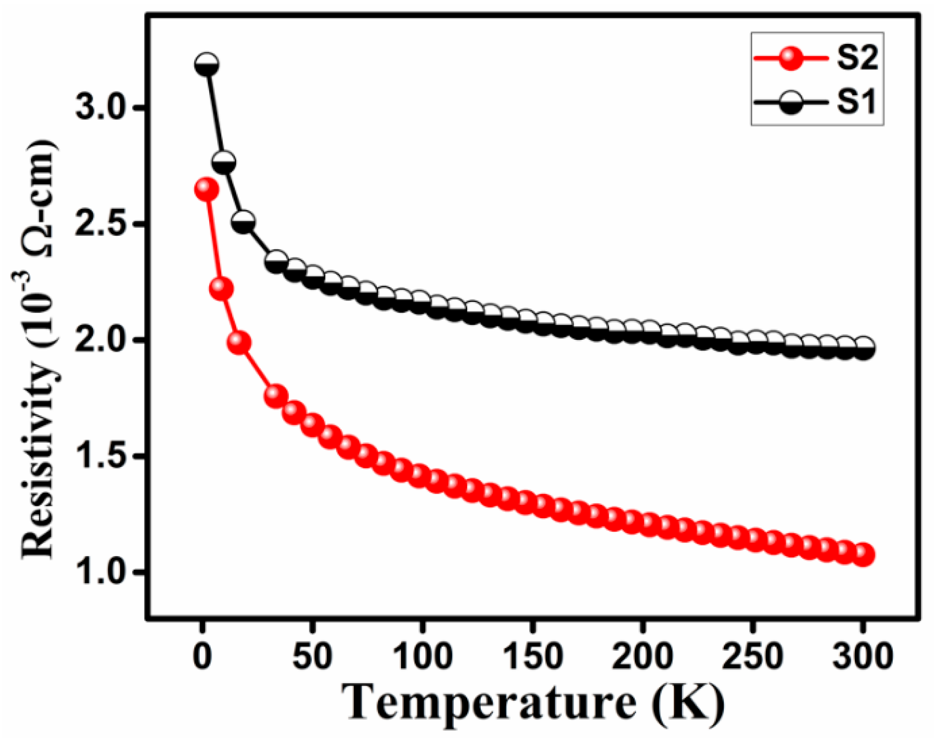
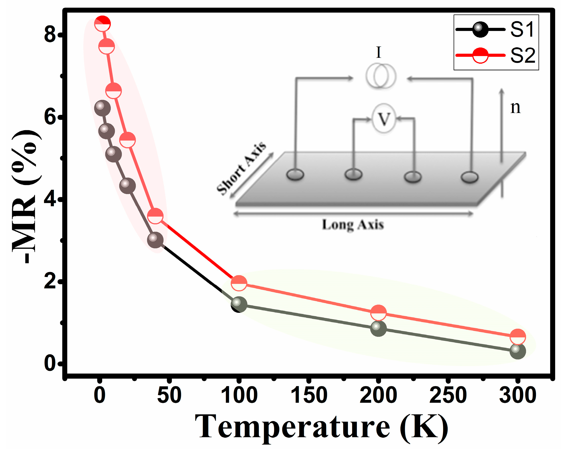
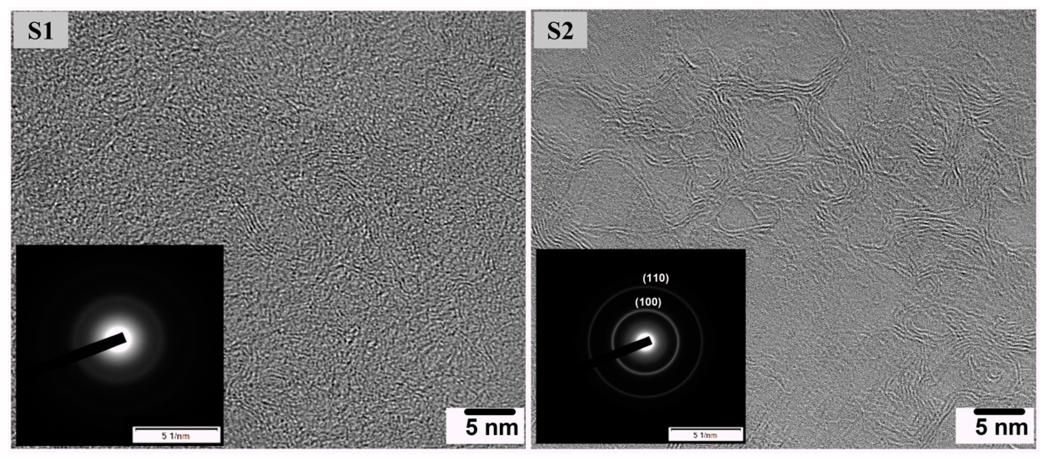
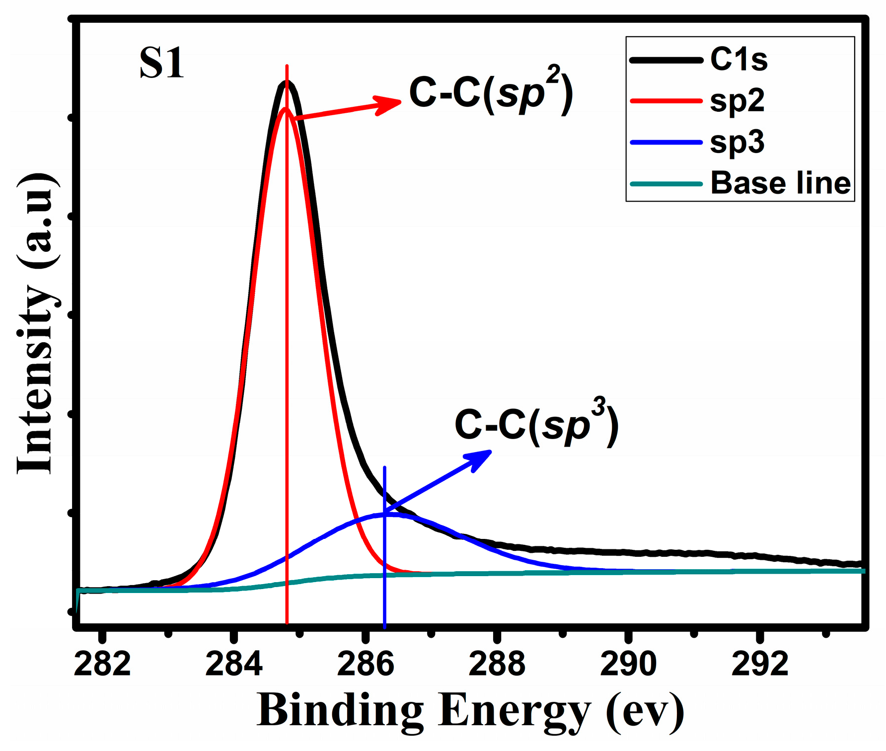
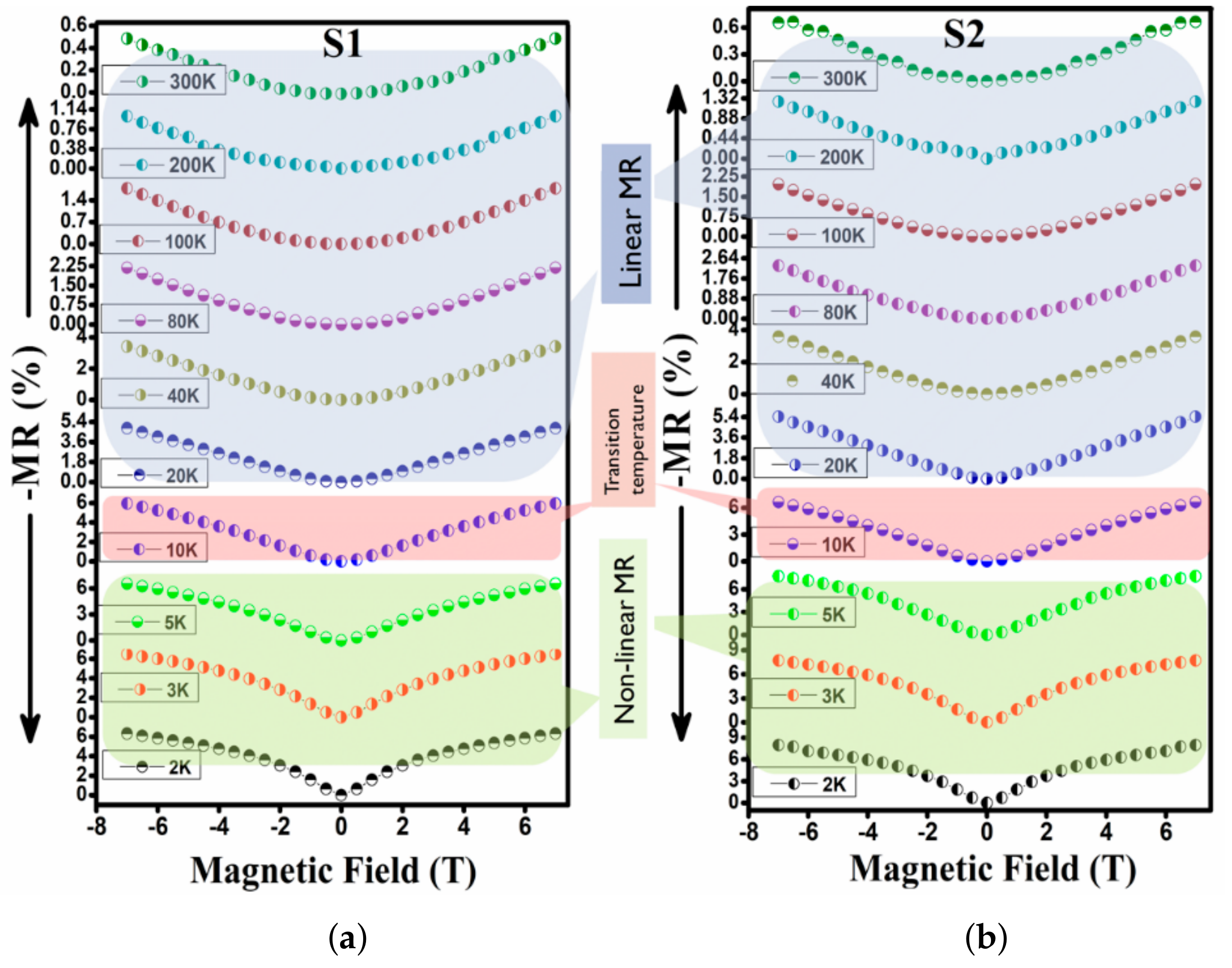
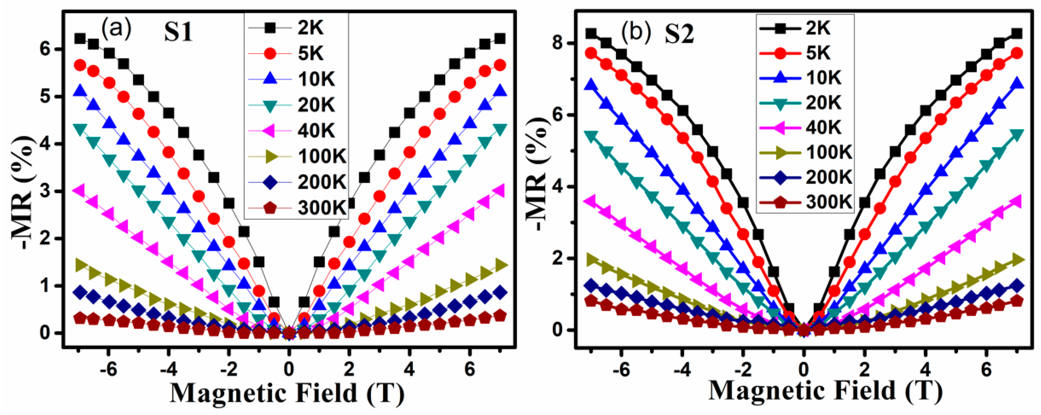
3. Results and Discussion
4. Conclusions
Author Contributions
Funding
Acknowledgments
Conflicts of Interest
References
- Fredriksson, H. Nanostructures of Graphite and Amorphous Carbon–Fabrication and Properties; Chalmers University of Technology: Goöteborg, Sweden, 2009. [Google Scholar]
- Harris, P.J.F. New Perspectives on the Structure of Graphitic Carbons. Crit. Rev. Solid State Mater. Sci. 2005, 30, 235–253. [Google Scholar] [CrossRef]
- Jacob, W.; Möller, W. On the structure of thin hydrocarbon films. Appl. Phys. Lett. 1993, 63, 1771–1773. [Google Scholar] [CrossRef]
- Chung, D.D. Carbon Fibers, Nanofibers, and Nanotubes. In Carbon Composites; Elsevier BV: Amsterdam, The Netherlands, 2017; pp. 1–87. [Google Scholar] [CrossRef]
- Hishiyama, Y.; Irumano, H.; Kaburagi, Y.; Soneda, Y. Structure, Raman scattering, and transport properties of boron-doped graphite. Phys. Rev. B 2001, 63, 245406. [Google Scholar] [CrossRef]
- Kamalakar, M.V.; Groenveld, C.; Dankert, A.; Dash, S.P. Long distance spin communication in chemical vapour deposited graphene. Nat. Commun. 2015, 6, 6766. [Google Scholar] [CrossRef]
- Robertson, J. Diamond-like amorphous carbon. Mater. Sci. Eng. R Rep. 2002, 37, 129–281. [Google Scholar] [CrossRef]
- Sagar, R.U.R.; Saleemi, A.S.; Zhang, X. Angular magnetoresistance in semiconducting undoped amorphous carbon thin films. J. Appl. Phys. 2015, 117, 174503. [Google Scholar] [CrossRef]
- Saleemi, A.S.; Singh, R.; Sun, W.; Luo, Z.; Zhang, X. Large magnetoresistance of amorphous carbon films. Carbon 2017, 122, 122–127. [Google Scholar] [CrossRef]
- Mahmood, A.; Yang, C.-S.; Dayen, J.-F.; Park, S.; Kamalakar, M.V.; Metten, D.; Berciaud, S.; Lee, J.-O.; Doudin, B. Room temperature dry processing of patterned CVD graphene devices. Carbon 2015, 86, 256–263. [Google Scholar] [CrossRef]
- Shabbir, B.; Wang, X.; Ghorbani, S.R.; Shekhar, C.; Dou, S.; Srivastava, O.N. Hydrostatic pressure: A very effective approach to significantly enhance critical current density in granular iron pnictide superconductors. Sci. Rep. 2015, 5, 8213. [Google Scholar] [CrossRef]
- Yakushiji, K.; Ernult, F.; Imamura, H.; Yamane, K.; Mitani, S.; Takanashi, K.; Takahashi, S.; Maekawa, S.; Fujimori, H. Enhanced spin accumulation and novel magnetotransport in nanoparticles. Nat. Mater. 2005, 4, 57–61. [Google Scholar] [CrossRef]
- Fan, Z.; Li, P.; Zhang, L.; Mi, W.; Jiang, E.; Bai, H. Electrical transport properties and room-temperature positive magnetoresistance of Fe3O4/a-C/n-Si junctions. Thin Solid Films 2012, 520, 3641–3646. [Google Scholar] [CrossRef]
- Godel, F.; Kamalakar, M.V.; Doudin, B.; Henry, Y.; Halley, D.; Dayen, J.-F. Voltage-controlled inversion of tunnel magnetoresistance in epitaxial nickel/graphene/MgO/cobalt junctions. Appl. Phys. Lett. 2014, 105, 152407. [Google Scholar] [CrossRef]
- Serrano, I.G.; Panda, J.; Denoel, F.; Vallin, Ö.; Phuyal, D.; Karis, O.; Kamalakar, M.V. Two-dimensional flexible high diffusive spin circuits. Nano Lett. 2019, 19, 666–673. [Google Scholar] [CrossRef] [PubMed]
- Wan, C.; Zhang, X.; Vanacken, J.; Gao, X.; Zhang, X.; Wu, L.; Tan, X.; Lin, H.; Moshchalkov, V.V.; Yuan, J. Electro- and magneto-transport properties of amorphous carbon films doped with iron. Diam. Relat. Mater. 2011, 20, 26–30. [Google Scholar] [CrossRef]
- Shabbir, B.; Malik, M.I.; A Khan, N. Effect on Diamagnetism and Phonon Modes due to Mg and Be Doping at Ca Sites in Cu0.5Tl0.5Ba2Ca3−y M y Cu4O12−δ (y = 0 and 1.5 for M = Mg, Be) High Temperature Superconductors. J. Supercond. Nov. Magn. 2011, 24, 1977–1983. [Google Scholar] [CrossRef]
- Shabbir, B.; Nadeem, M.; Dai, Z.; Fuhrer, M.S.; Xue, Q.-K.; Wang, X.; Bao, Q. Long range intrinsic ferromagnetism in two dimensional materials and dissipationless future technologies. Appl. Phys. Rev. 2018, 5, 041105. [Google Scholar] [CrossRef]
- Zeb, M.H.; Shabbir, B.; Sagar, R.U.R.; Mahmood, N.; Chen, K.; Qasim, I.; Malik, M.I.; Yu, W.; Hossain, M.M.; Dai, Z.; et al. Superior magnetoresistance performance of hybrid graphene foam/metal sulfide nanocrystal devices. ACS Appl. Mater. Interfaces 2019, 11, 19397–19403. [Google Scholar] [CrossRef]
- Shabbir, B.; Huang, H.; Yao, C.; Ma, Y.; Dou, S.; Johansen, T.H.; Hosono, H.; Wang, X. Evidence for superior current carrying capability of iron pnictide tapes under hydrostatic pressure. Phys. Rev. Mater. 2017, 1, 044805. [Google Scholar] [CrossRef]
- Sagar, R.U.R.; Qazi, H.I.A.; Zeb, M.H.; Stadler, F.J.; Shabbir, B.; Wang, X.; Zhang, M. Tunable sign of magnetoresistance in graphene foam—Ecoflex® composite for wearable magnetoelectronic devices. Mater. Lett. 2019, 253, 166–170. [Google Scholar] [CrossRef]
- Hu, B.; Wu, Y. Tuning magnetoresistance between positive and negative values in organic semiconductors. Nat. Mater. 2007, 6, 985–991. [Google Scholar] [CrossRef]
- Zhang, X.; Zhang, X.; Wan, C.; Wu, L. A bias voltage dependent positive magnetoresistance in Co[sub x]–C[sub 1−x]/Si heterostructure. Appl. Phys. Lett. 2009, 95, 22503. [Google Scholar] [CrossRef]
- Saleemi, A.S.; Sun, W.; Singh, R.; Luo, Z.; Zhang, X. Structure dependent negative and positive magnetoresistance of amorphous carbon films. J. Appl. Phys. 2017, 121, 233903. [Google Scholar] [CrossRef]
- Wang, J.; Zhang, X.; Wan, C.; Vanacken, J.; Moshchalkov, V.V. Magnetotransport properties of undoped amorphous carbon films. Carbon 2013, 59, 278–282. [Google Scholar] [CrossRef]
- Saleemi, A.S.; Sagar, R.U.R.; Singh, R.; Luo, Z.; Zhang, X. Angle dependent magnetotransport in transfer-free amorphous carbon thin films. J. Phys. D Appl. Phys. 2016, 49, 415005. [Google Scholar] [CrossRef]
- Wu, S.; Liu, Y.; Ge, Y.; Ran, L.; Peng, K.; Yi, M. Structural transformation of carbon/carbon composites for aircraft brake pairs in the braking process. Tribol. Int. 2016, 102, 497–506. [Google Scholar] [CrossRef]
- Ferrari, A.C.; Robertson, J. Interpretation of Raman spectra of disordered and amorphous carbon. Phys. Rev. B 1999, 61, 14095. [Google Scholar] [CrossRef]
- Robertson, J.; Ferrari, A.C. Raman spectroscopy of amorphous, nanostructured, diamond–like carbon, and nanodiamond. Philos. Trans. R. Soc. A Math. Phys. Eng. Sci. 2004, 362, 2477–2512. [Google Scholar] [CrossRef]
- Zhang, X.; Xue, Q.; Zhu, D. Positive and negative linear magnetoresistance of graphite. Phys. Lett. A 2004, 320, 471–477. [Google Scholar] [CrossRef]
- Xue, Q.; Zhang, X. Anomalous electrical transport properties of amorphous carbon films on Si substrates. Carbon 2005, 43, 760–764. [Google Scholar] [CrossRef]


© 2019 by the authors. Licensee MDPI, Basel, Switzerland. This article is an open access article distributed under the terms and conditions of the Creative Commons Attribution (CC BY) license (http://creativecommons.org/licenses/by/4.0/).
Share and Cite
Saleemi, A.S.; Saeed, M.; Hussan, M.; Rehman, S.U.; Hafeez, M.; Mehmood, S.; Sial, M.A.Z.G.; Lee, S.-l. Anomalous Non-Linear to Linear Shift in Magnetoresistance of Amorphous Carbon Films. Crystals 2019, 9, 618. https://doi.org/10.3390/cryst9120618
Saleemi AS, Saeed M, Hussan M, Rehman SU, Hafeez M, Mehmood S, Sial MAZG, Lee S-l. Anomalous Non-Linear to Linear Shift in Magnetoresistance of Amorphous Carbon Films. Crystals. 2019; 9(12):618. https://doi.org/10.3390/cryst9120618
Chicago/Turabian StyleSaleemi, Awais Siddique, Muhammad Saeed, Muhammad Hussan, Shafiq Ur Rehman, Muhammad Hafeez, Shahid Mehmood, M. Aurang Zeb Gul Sial, and Shern-long Lee. 2019. "Anomalous Non-Linear to Linear Shift in Magnetoresistance of Amorphous Carbon Films" Crystals 9, no. 12: 618. https://doi.org/10.3390/cryst9120618
APA StyleSaleemi, A. S., Saeed, M., Hussan, M., Rehman, S. U., Hafeez, M., Mehmood, S., Sial, M. A. Z. G., & Lee, S.-l. (2019). Anomalous Non-Linear to Linear Shift in Magnetoresistance of Amorphous Carbon Films. Crystals, 9(12), 618. https://doi.org/10.3390/cryst9120618