A Study on the Growth Window of Polycrystalline Diamond on Si3N4-coated N-Polar GaN


Abstract
1. Introduction
2. Materials and Methods
3. Results and Discussion
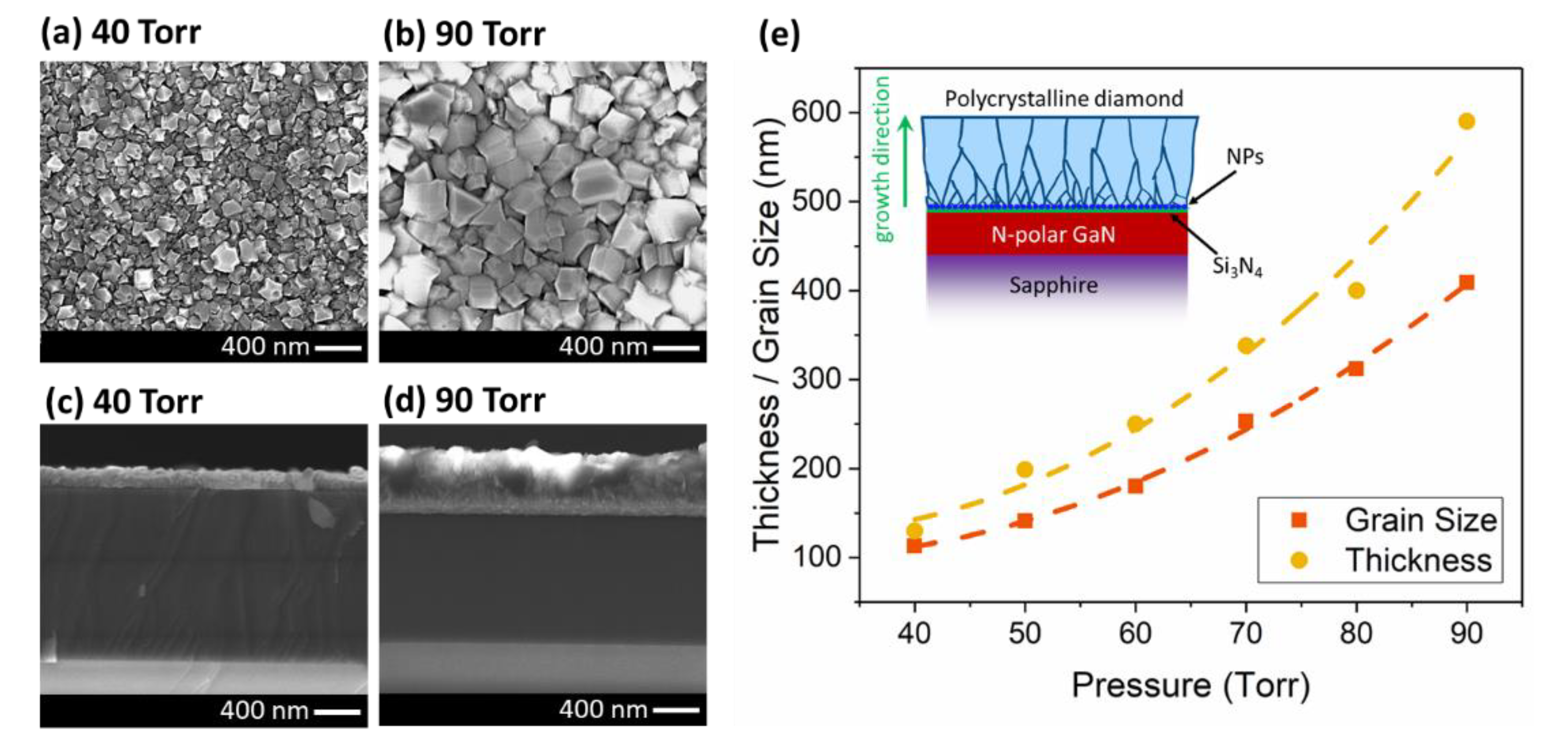
3.1. Grain Size and Thickness
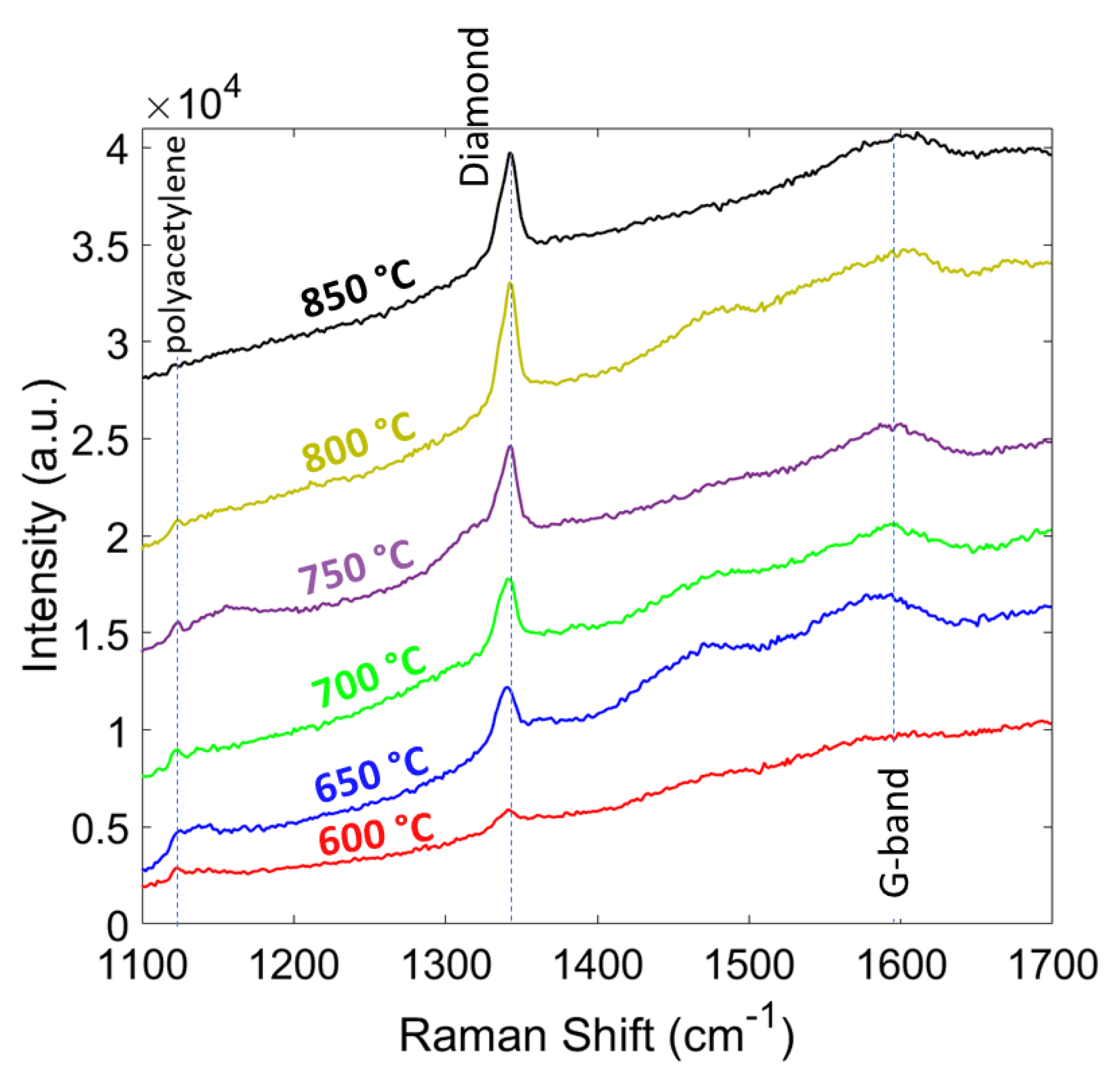
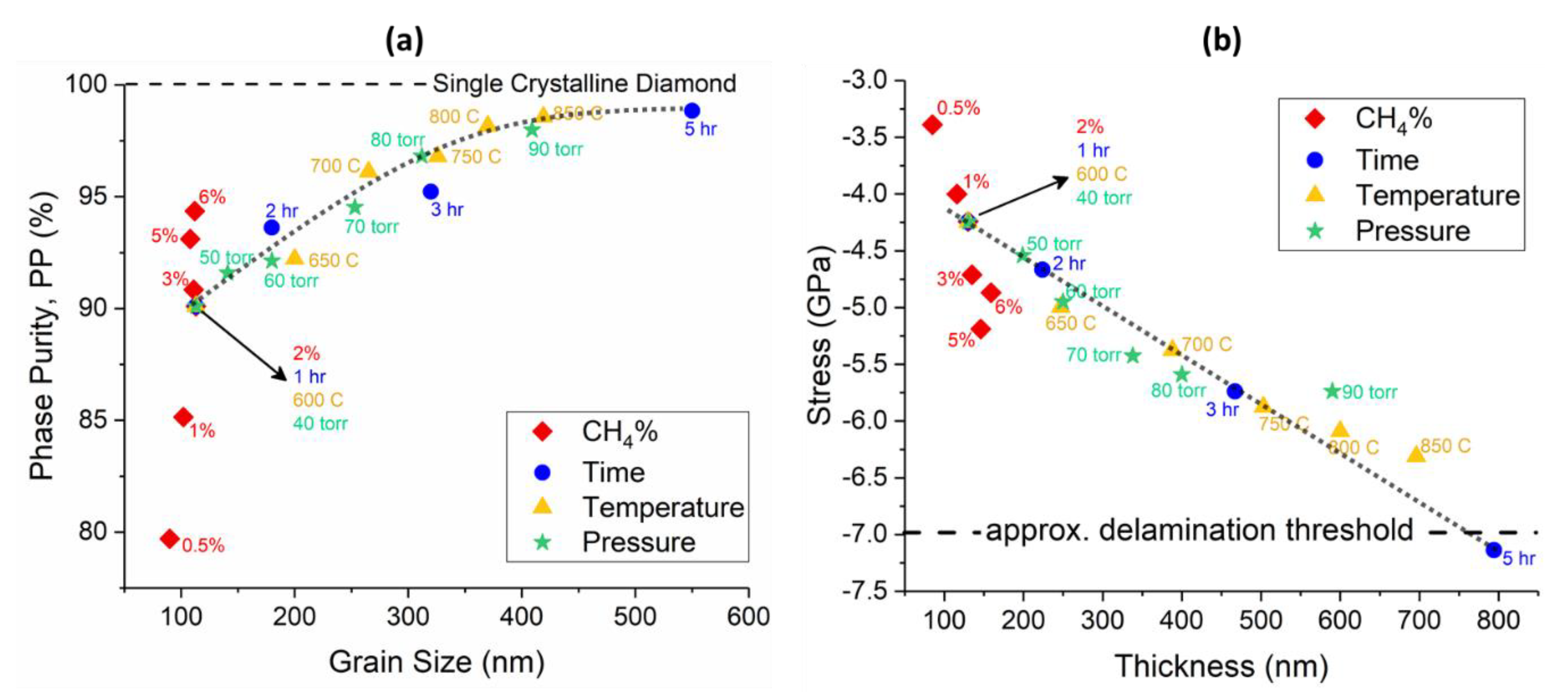
3.2. Phase Purity and Residual Stress
4. Conclusions
Author Contributions
Funding
Acknowledgments
Conflicts of Interest
References
- Davies, G. Basic Properties of Diamond: Phonon Spectra, Thermal Properties, Band Structure. In CVD Diamond for Electronic Devices and Sensors; Sussmann, R.S., Ed.; John Wiley & Sons Ltd: West Sussex, UK, 2009; pp. 3–28. ISBN 9780470065327. [Google Scholar]
- Celii, F.G.; Butler, J.E. Diamond chemical vapor deposition. Annu. Rev. Phys. Chern. 1991, 42, 643–684. [Google Scholar] [CrossRef]
- Green, B.M.; Chu, K.K.; Chumbes, E.M.; Smart, J.A.; Shealy, J.R.; Eastman, L.F. The effect of surface passivation on the microwave characteristics of undoped AlGaN/GaN HEMT’s. IEEE Electron Device Lett. 2000, 21, 268–270. [Google Scholar] [CrossRef]
- Wu, Y.F.; Kapolnek, D.; Ibbetson, J.P.; Parikh, P.; Keller, B.P.; Mishra, U.K. Very-high power density AlGaN/GaN HEMTs. IEEE Trans. Electron Devices 2001, 48, 586–590. [Google Scholar]
- Chung, J.W.; Hoke, W.E.; Chumbes, E.M.; Palacios, T. AlGaN/GaN HEMT with 300-GHz fmax. IEEE Electron Device Lett. 2010, 31, 195–197. [Google Scholar] [CrossRef]
- Mishra, U.K.; Parikh, P.; Wu, Y.F. AlGaN/GaN HEMTs—An overview of device operation and applications. Proc. IEEE 2002, 90, 1022–1031. [Google Scholar] [CrossRef]
- Shen, L.; Heikman, S.; Moran, B.; Coffie, R.; Zhang, N.Q.; Buttari, D.; Smorchkova, I.P.; Keller, S.; DenBaars, S.P.; Mishra, U.K. AlGaN/AlN/GaN high-power microwave HEMT. IEEE Electron Device Lett. 2001, 22, 457–459. [Google Scholar] [CrossRef]
- Zheng, X.; Li, H.; Ahmadi, E.; Hestroffer, K.; Guidry, M.; Romanczyk, B.; Wienecke, S.; Keller, S.; Mishra, U.K. High frequency N-polar GaN planar MIS-HEMTs on sapphire with high breakdown and low dispersion. In Proceedings of the 2016 Lester Eastman Conference (LEC), Bethlehem, PA, USA, 2–4 August 2016; IEEE: Bethlehem, PA, USA, 2016; pp. 42–45. [Google Scholar]
- Koksaldi, O.S.; Haller, J.; Li, H.; Romanczyk, B.; Guidry, M.; Wienecke, S.; Keller, S.; Mishra, U.K. N-Polar GaN HEMTs exhibiting record breakdown voltage over 2000 v and Low Dynamic On-Resistance. IEEE Electron Device Lett. 2018, 39, 1014–1017. [Google Scholar] [CrossRef]
- Wong, M.H.; Keller, S.; Dasgupta, N.S.; Denninghoff, D.J.; Kolluri, S.; Brown, D.F.; Lu, J.; Fichtenbaum, N.A.; Ahmadi, E.; Singisetti, U.; et al. N-polar GaN epitaxy and high electron mobility transistors. Semicond. Sci. Technol. 2013, 28, 074009. [Google Scholar] [CrossRef]
- Wienecke, S.; Romanczyk, B.; Guidry, M.; Li, H.; Ahmadi, E.; Hestroffer, K.; Zheng, X.; Keller, S.; Mishra, U.K. N-polar GaN cap MISHEMT with Record Power Density Exceeding 6.5 W/mm at 94 GHz. IEEE Electron Device Lett. 2017, 38, 359–362. [Google Scholar] [CrossRef]
- Gaska, R.; Osinsky, A.; Yang, J.W.; Shur, M.S. Self-heating in high-power AlGaN-GaN HFET’s. IEEE Electron Device Lett. 1998, 19, 89–91. [Google Scholar] [CrossRef]
- Wang, X.D.; Hu, W.D.; Chen, X.S.; Lu, W. The study of self-heating and hot-electron effects for AlGaN/GaN double-channel HEMTs. IEEE Trans. Electron Devices 2012, 59, 1393–1401. [Google Scholar] [CrossRef]
- Kuball, M.; Hayes, J.M.; Uren, M.J.; Martin, T.; Birbeck, J.C.H.; Balmer, R.S.; Hughes, B.T. Measurement of temperature in active high-power AlGaN/GaN HFETs using Raman spectroscopy. IEEE Electron Device Lett. 2002, 23, 7–9. [Google Scholar] [CrossRef]
- Kolluri, S.; Keller, S.; Denbaars, S.P.; Mishra, U.K. N-polar GaN MIS-HEMTs with a 12.1-W/mm continuous-wave output power density at 4 GHz on sapphire substrate. IEEE Electron Device Lett. 2011, 32, 635–637. [Google Scholar] [CrossRef]
- Jessen, G.H.; Gillespie, J.K.; Via, G.D.; Crespo, A.; Langley, D.; Wasserbauer, J.; Faili, F.; Francis, D.; Babic, D.; Ejeckam, F.; et al. AlGaN/GaN HEMT on diamond technology demonstration. In Proceedings of the Technical Digest—IEEE Compound Semiconductor Integrated Circuit Symposium (CSICS), San Antonio, TX, USA, 12–15 November 2006; pp. 271–274. [Google Scholar]
- Dumka, D.C.; Chou, T.M.; Jimenez, J.L.; Fanning, D.M.; Francis, D.; Faili, F.; Ejeckam, F.; Bernardoni, M.; Pomeroy, J.W.; Kuball, M. Electrical and thermal performance of AlGaN/GaN HEMTs on diamond substrate for RF applications. In Proceedings of the 2013 IEEE Compound Semiconductor Integrated Circuit Symposium (CSICS), Monterey, CA, USA, 13–16 October 2013; IEEE: Monterey, CA, USA, 2013; pp. 1–4. [Google Scholar]
- Ohki, T.; Yamada, A.; Minoura, Y.; Makiyama, K.; Kotani, J.; Ozaki, S.; Sato, M.; Okamoto, N.; Joshin, K.; Nakamura, N. An over 20-W/mm S-Band InAlGaN/GaN HEMT with SiC/Diamond-Bonded Heat Spreader. IEEE Electron Device Lett. 2019, 40, 287–290. [Google Scholar] [CrossRef]
- Alomari, M.; Dipalo, M.; Rossi, S.; Diforte-Poisson, M.A.; Delage, S.; Carlin, J.F.; Grandjean, N.; Gaquiere, C.; Toth, L.; Pecz, B.; et al. Diamond overgrown InAlN/GaN HEMT. Diam. Relat. Mater. 2011, 20, 604–608. [Google Scholar] [CrossRef]
- Anderson, T.J.; Koehler, A.D.; Hobart, K.D.; Tadjer, M.J.; Feygelson, T.I.; Hite, J.K.; Pate, B.B.; Kub, F.J.; Eddy, C.R. Nanocrystalline diamond-gated AlGaN/GaN HEMT. IEEE Electron Device Lett. 2013, 34, 1382–1384. [Google Scholar] [CrossRef]
- Tadjer, M.J.; Anderson, T.J.; Hobart, K.D.; Feygelson, T.I.; Caldwell, J.D.; Eddy, C.R.; Kub, F.J.; Butler, J.E.; Pate, B.; Melngailis, J. Reduced self-heating in AlGaN/GaN HEMTs using nanocrystalline diamond heat-spreading films. IEEE Electron Device Lett. 2012, 33, 23–25. [Google Scholar] [CrossRef]
- Zhou, Y.; Ramaneti, R.; Anaya, J.; Korneychuk, S.; Derluyn, J.; Sun, H.; Pomeroy, J.; Verbeeck, J.; Haenen, K.; Kuball, M. Thermal characterization of polycrystalline diamond thin film heat spreaders grown on GaN HEMTs. Appl. Phys. Lett. 2017, 111. [Google Scholar] [CrossRef]
- Liu, H.; Li, J.; Li, Z.; Xu, K.; Chen, Z.; Chen, G. Single Crystal Diamond Deposited by Dual Radio-Frequency Plasma Jet CVD with High Growth Rate. Crystals 2019, 9, 32. [Google Scholar] [CrossRef]
- Wang, Q.; Wu, G.; Liu, S.; Gan, Z.; Yang, B.; Pan, J. Simulation-Based Development of a new cylindrical-cavity microwave-plasma reactor for diamond-film synthesis. Crystals 2019, 9, 320. [Google Scholar] [CrossRef]
- Ashkinazi, E.E.; Khmelnitskii, R.A.; Sedov, V.S.; Khomich, A.A.; Khomich, A.V.; Ralchenko, V.G. Morphology of diamond layers grown on different facets of single crystal diamond substrates by a microwave plasma CVD in CH4-H2-N2 gas mixtures. Crystals 2017, 7, 166. [Google Scholar] [CrossRef]
- Yates, L.; Anderson, J.; Gu, X.; Lee, C.; Bai, T.; Mecklenburg, M.; Aoki, T.; Goorsky, M.S.; Kuball, M.; Piner, E.L.; et al. Low thermal boundary resistance interfaces for GaN-On-Diamond devices. ACS Appl. Mater. Interfaces 2018, 10, 24302–24309. [Google Scholar] [CrossRef] [PubMed]
- Zou, Y.S.; Yang, Y.; Chong, Y.M.; Ye, Q.; He, B.; Yao, Z.Q.; Zhang, W.J.; Lee, S.T.; Cai, Y.; Chu, H.S. Chemical vapor deposition of diamond films on patterned GaN substrates via a thin silicon nitride protective layer. Cryst. Growth Des. 2008, 8, 1770–1773. [Google Scholar] [CrossRef]
- Seelmann-eggebert, M.; Meisen, P.; Schaudel, F.; Koidl, P.; Vescan, A. Heat-spreading diamond films for GaN-based high-power transistor devices. Diam. Relat. Mater. 2001, 10, 744–749. [Google Scholar] [CrossRef]
- Graebner, J.E.; Jin, S.; Kammlott, G.W.; Herbt, J.A.; Gardiniert, C.F. Large anisotropic thermal conductivity in synthetic diamond films. Nature 1992, 359, 401–403. [Google Scholar] [CrossRef]
- Sood, A.; Cho, J.; Hobart, K.D.; Feygelson, T.I.; Pate, B.B.; Asheghi, M.; Cahill, D.G.; Goodson, K.E. Anisotropic and inhomogeneous thermal conduction in suspended thin-film polycrystalline diamond. J. Appl. Phys. 2016, 119, 175103. [Google Scholar] [CrossRef]
- Angadi, M.A.; Watanabe, T.; Bodapati, A.; Xiao, X.; Auciello, O.; Carlisle, J.A.; Eastman, J.A.; Keblinski, P.; Schelling, P.K.; Phillpot, S.R. Thermal transport and grain boundary conductance in ultrananocrystalline diamond thin films. J. Appl. Phys. 2006, 99. [Google Scholar] [CrossRef]
- Guillemet, T.; Xie, Z.Q.; Zhou, Y.S.; Park, J.B.; Veillere, A.; Xiong, W.; Heintz, J.M.; Silvain, J.F.; Chandra, N.; Lu, Y.F. Stress and phase purity analyses of diamond films deposited through laser-assisted combustion synthesis. ACS Appl. Mater. Interfaces 2011, 3, 4120–4125. [Google Scholar] [CrossRef]
- Keller, S.; Parish, G.; Fini, P.T.; Heikman, S.; Chen, C.H.; Zhang, N.; DenBaars, S.P.; Mishra, U.K.; Wu, Y.F. Metalorganic chemical vapor deposition of high mobility AlGaN/GaN heterostructures. J. Appl. Phys. 1999, 86, 5850–5857. [Google Scholar] [CrossRef]
- Keller, S.; Li, H.; Laurent, M.; Hu, Y.; Pfaff, N.; Lu, J.; Brown, D.F.; Fichtenbaum, N.A.; Speck, J.S.; Denbaars, S.P.; et al. Recent progress in metal-organic chemical vapor deposition of N-polar group-III nitrides. Semicond. Sci. Technol. 2014, 29, 113001. [Google Scholar] [CrossRef]
- Girard, H.A.; Perruchas, S.; Gesset, C.; Chaigneau, M.; Vieille, L.; Arnault, J.C.; Bergonzo, P.; Boilot, J.P.; Gacoin, T. Electrostatic grafting of diamond nanoparticles: A versatile route to nanocrystalline diamond thin films. ACS Appl. Mater. Interfaces 2009, 1, 2738–2746. [Google Scholar] [CrossRef] [PubMed]
- Laurent, M.A.; Malakoutian, M.; Chowdhury, S. A study on the nucleation and MPCVD growth of thin, dense, and contiguous nanocrystalline diamond films on bare and Si3N4-coated N-polar GaN. Submitt. Semicond. Sci. Technol. 2019. [Google Scholar]
- Thomas, E.L.H.; Mandal, S.; Ashek-I-Ahmed; MacDonald, J.E.; Dane, T.G.; Rawle, J.; Cheng, C.L.; Williams, O.A. Spectroscopic ellipsometry of nanocrystalline diamond film growth. ACS Omega 2017, 2, 6715–6727. [Google Scholar] [CrossRef] [PubMed]
- Sternschulte, H.; Bauer, T.; Schreck, M.; Stritzker, B. Comparison of MWPCVD diamond growth at low and high process gas pressures. Diam. Relat. Mater. 2006, 15, 542–547. [Google Scholar] [CrossRef]
- Drift, A. Van der Evolutionary selection, a principle governing growth orientation in vapour-deposited layers. Philips Res. Rep. 1967, 22, 267–288. [Google Scholar]
- Chen, Y.C.; Chang, L. Chemical vapor deposition of diamond on an adamantane-coated sapphire substrate. RSC Adv. 2014, 4, 18945–18950. [Google Scholar] [CrossRef]
- Osswald, S.; Mochalin, V.N.; Havel, M.; Yushin, G.; Gogotsi, Y. Phonon confinement effects in the Raman spectrum of nanodiamond. Phys. Rev. B-Condens. Matter Mater. Phys. 2009, 80, 075419. [Google Scholar] [CrossRef]
- Williams, O.A.; Nesladek, M.; Daenen, M.; Michaelson, S.; Hoffman, A.; Osawa, E.; Haenen, K.; Jackman, R.B. Growth, electronic properties and applications of nanodiamond. Diam. Relat. Mater. 2008, 17, 1080–1088. [Google Scholar] [CrossRef]
- Pimenta, M.A.; Dresselhaus, G.; Dresselhaus, M.S.; Cancado, L.G.; Jorio, A.; Saito, R. Studying disorder in graphite-based systems by Raman spectroscopy. Phys. Chem. Chem. Phys. 2007, 9, 1276–1291. [Google Scholar] [CrossRef]
- Eckert, M.; Neyts, E.; Bogaerts, A. Insights into the growth of (ultra)nanocrystalline diamond by combined molecular dynamics and Monte Carlo simulations. Cryst. Growth Des. 2010, 10, 3005–3021. [Google Scholar] [CrossRef]
- Tu, R.; Xu, T.; Li, D.; Zhang, S.; Yang, M.; Li, Q.; Zhang, L.; Shimada, T.; Goto, T.; Shi, J. Morphology and mechanical behavior of diamond films fabricated by IH-MPCVD. RSC Adv. 2018, 8, 16061–16068. [Google Scholar] [CrossRef]
- Wada, N.; Solin, S.A. Raman efficiency measurements of graphite. Phys. B + C 1981, 105, 353–356. [Google Scholar] [CrossRef]
- Shroder, R.E.; Nemanich, R.J.; Glass, J.T. Analysis ofthe composite structures in diamond thin films by Raman spectroscopy. Phys. Rev. B 1990, 41, 3738–3745. [Google Scholar] [CrossRef] [PubMed]
- Fortunato, W.; Chiquito, A.J.; Galzerani, J.C.; Moro, J.R. Crystalline quality and phase purity of CVD diamond films studied by Raman spectroscopy. J. Mater. Sci. 2007, 42, 7331–7336. [Google Scholar] [CrossRef]
- Ager, J.W.; Drory, M.D. Quantitative measurement of residual biaxial stress by Raman spectroscopy in diamond grown on a Ti alloy by chemical vapor deposition. Phys. Rev. B 1993, 48, 2601–2607. [Google Scholar] [CrossRef] [PubMed]


| CH4 (%) | Grain Size (nm) | Thickness (nm) | ϑm (cm−1) | PP (%) | Stress (GPa) |
|---|---|---|---|---|---|
| 0.5 | 90 | 85 | 1337.9 | 79.71 | −3.4 |
| 1 | 102 | 116 | 1339.0 | 85.15 | −4.0 |
| 2 | 113 | 130 | 1339.5 | 90.1 | −4.2 |
| 3 | 111 | 135 | 1340.3 | 90.84 | −4.7 |
| 5 | 108 | 146 | 1341.1 | 93.11 | −5.2 |
| 6 | 112 | 159 | 1340.6 | 94.36 | −4.9 |
| Pressure (Torr) | Grain Size (nm) | Thickness (nm) | ϑm (cm−1) | PP (%) | Stress (GPa) |
|---|---|---|---|---|---|
| 40 | 113 | 130 | 1339.5 | 90.1 | −4.2 |
| 50 | 141 | 199 | 1340.0 | 91.59 | −4.5 |
| 60 | 180 | 250 | 1340.7 | 92.13 | −4.9 |
| 70 | 253 | 338 | 1341.6 | 94.52 | −5.4 |
| 80 | 312 | 400 | 1341.9 | 96.81 | −5.6 |
| 90 | 409 | 590 | 1342.1 | 97.98 | −5.7 |
| Temperature (°C) | Grain Size (nm) | Thickness (nm) | ϑm (cm−1) | PP (%) | Stress (GPa) |
|---|---|---|---|---|---|
| 600 | 113 | 130 | 1339.5 | 90.1 | −4.2 |
| 650 | 200 | 247 | 1340.8 | 92.22 | −5.0 |
| 700 | 265 | 388 | 1341.5 | 96.11 | −5.4 |
| 750 | 326 | 503 | 1342.4 | 96.79 | −5.9 |
| 800 | 370 | 600 | 1342.7 | 98.16 | −6.1 |
| 850 | 419 | 696 | 1343.1 | 98.57 | −6.3 |
| Time (h) | Grain Size (nm) | Thickness (nm) | ϑm (cm−1) | PP (%) | Stress (GPa) |
|---|---|---|---|---|---|
| 1 | 113 | 130 | 1339.5 | 90.1 | −4.2 |
| 2 | 180 | 224 | 1340.2 | 93.61 | −4.6 |
| 3 | 320 | 467 | 1342.1 | 95.22 | −5.7 |
| 5 | 550 | 794 | 1344.6 | 98.84 | −7.1 |
© 2019 by the authors. Licensee MDPI, Basel, Switzerland. This article is an open access article distributed under the terms and conditions of the Creative Commons Attribution (CC BY) license (http://creativecommons.org/licenses/by/4.0/).
Share and Cite
Malakoutian, M.; Laurent, M.A.; Chowdhury, S. A Study on the Growth Window of Polycrystalline Diamond on Si3N4-coated N-Polar GaN. Crystals 2019, 9, 498. https://doi.org/10.3390/cryst9100498
Malakoutian M, Laurent MA, Chowdhury S. A Study on the Growth Window of Polycrystalline Diamond on Si3N4-coated N-Polar GaN. Crystals. 2019; 9(10):498. https://doi.org/10.3390/cryst9100498
Chicago/Turabian StyleMalakoutian, Mohamadali, Matthew A. Laurent, and Srabanti Chowdhury. 2019. "A Study on the Growth Window of Polycrystalline Diamond on Si3N4-coated N-Polar GaN" Crystals 9, no. 10: 498. https://doi.org/10.3390/cryst9100498
APA StyleMalakoutian, M., Laurent, M. A., & Chowdhury, S. (2019). A Study on the Growth Window of Polycrystalline Diamond on Si3N4-coated N-Polar GaN. Crystals, 9(10), 498. https://doi.org/10.3390/cryst9100498