Tuning the Size, Shape and Density of γ′-GayFe4−yN Nanocrystals Embedded in GaN


Abstract
1. Introduction
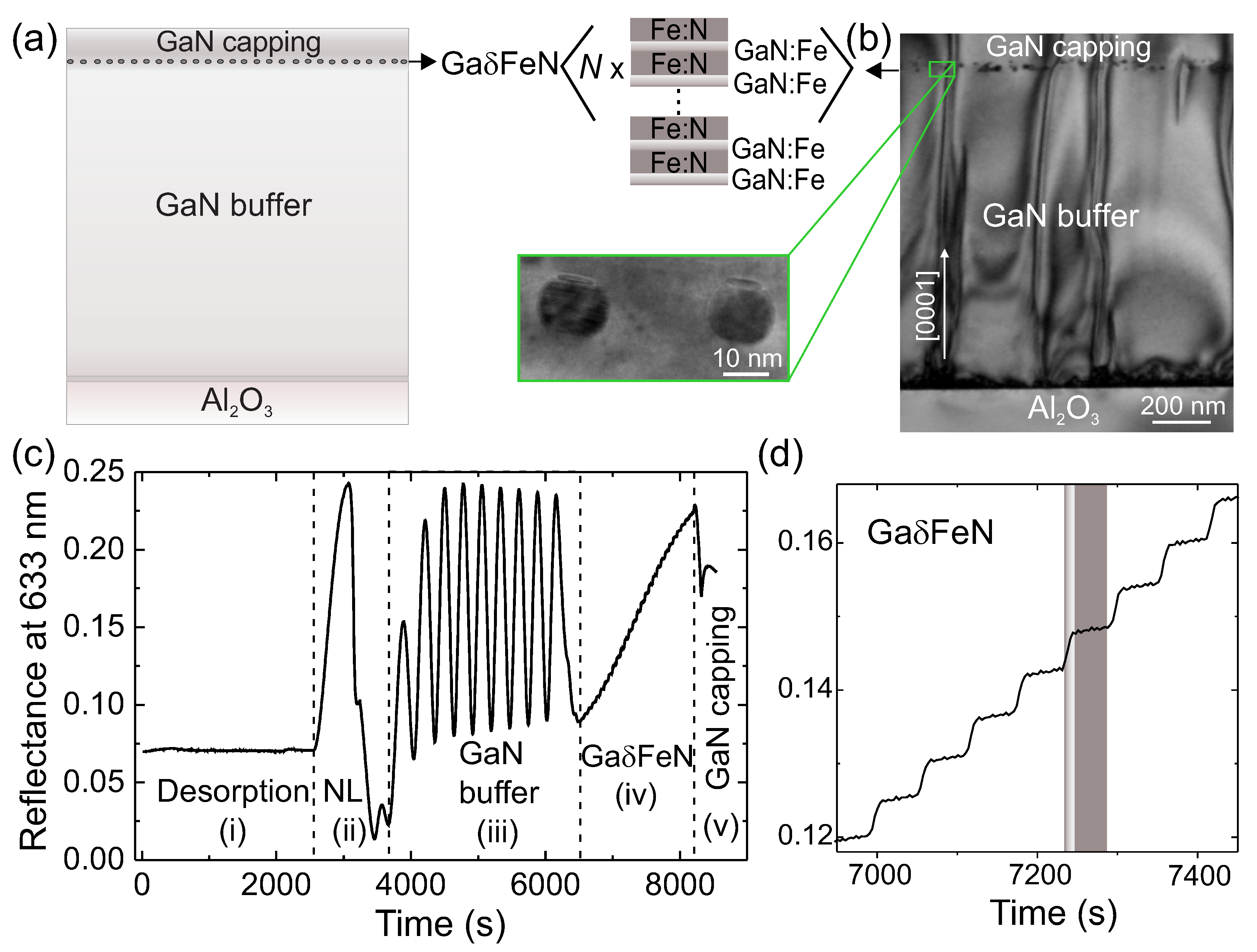
2. Materials and Methods
3. Results
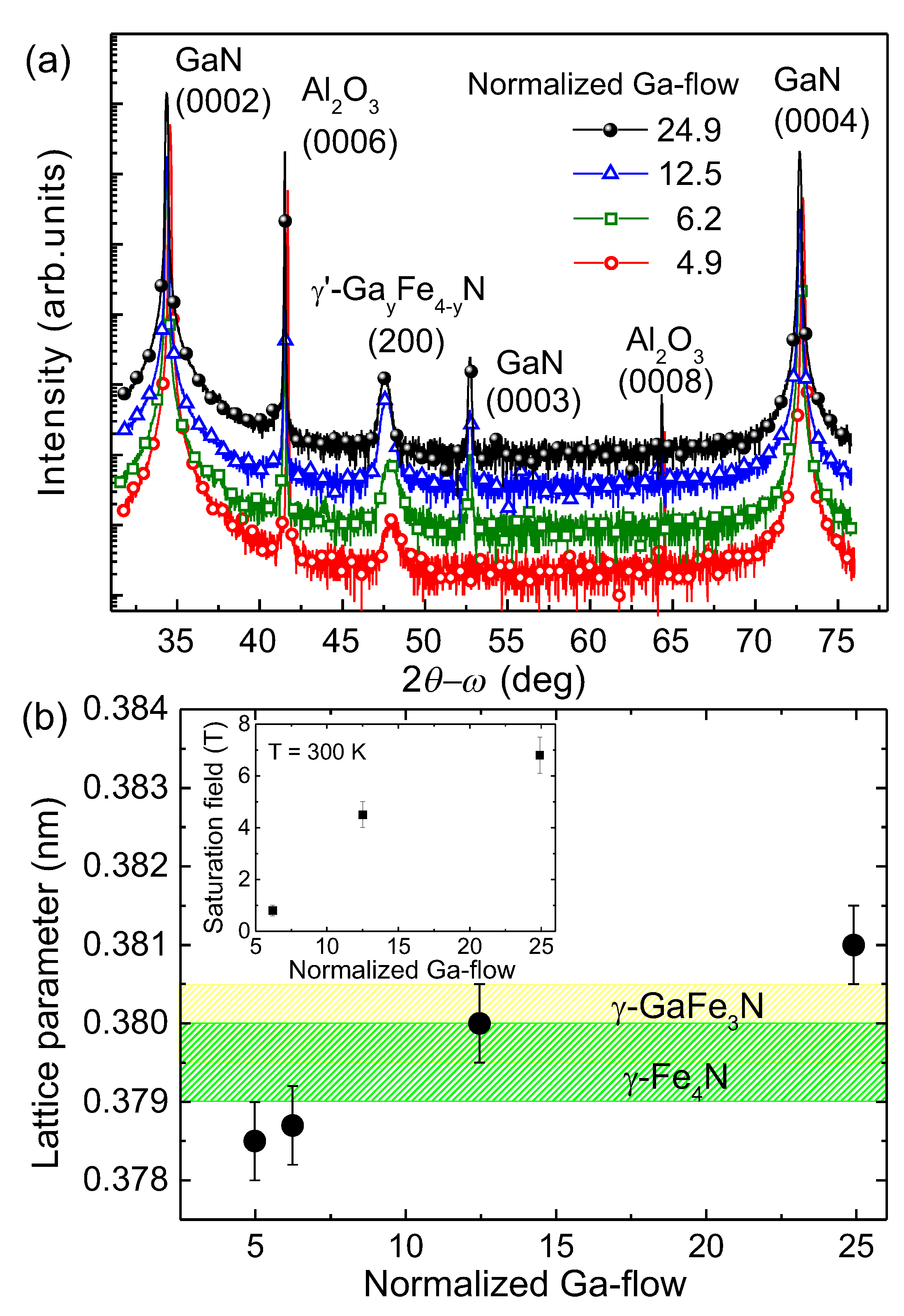
3.1. Crystal Structure
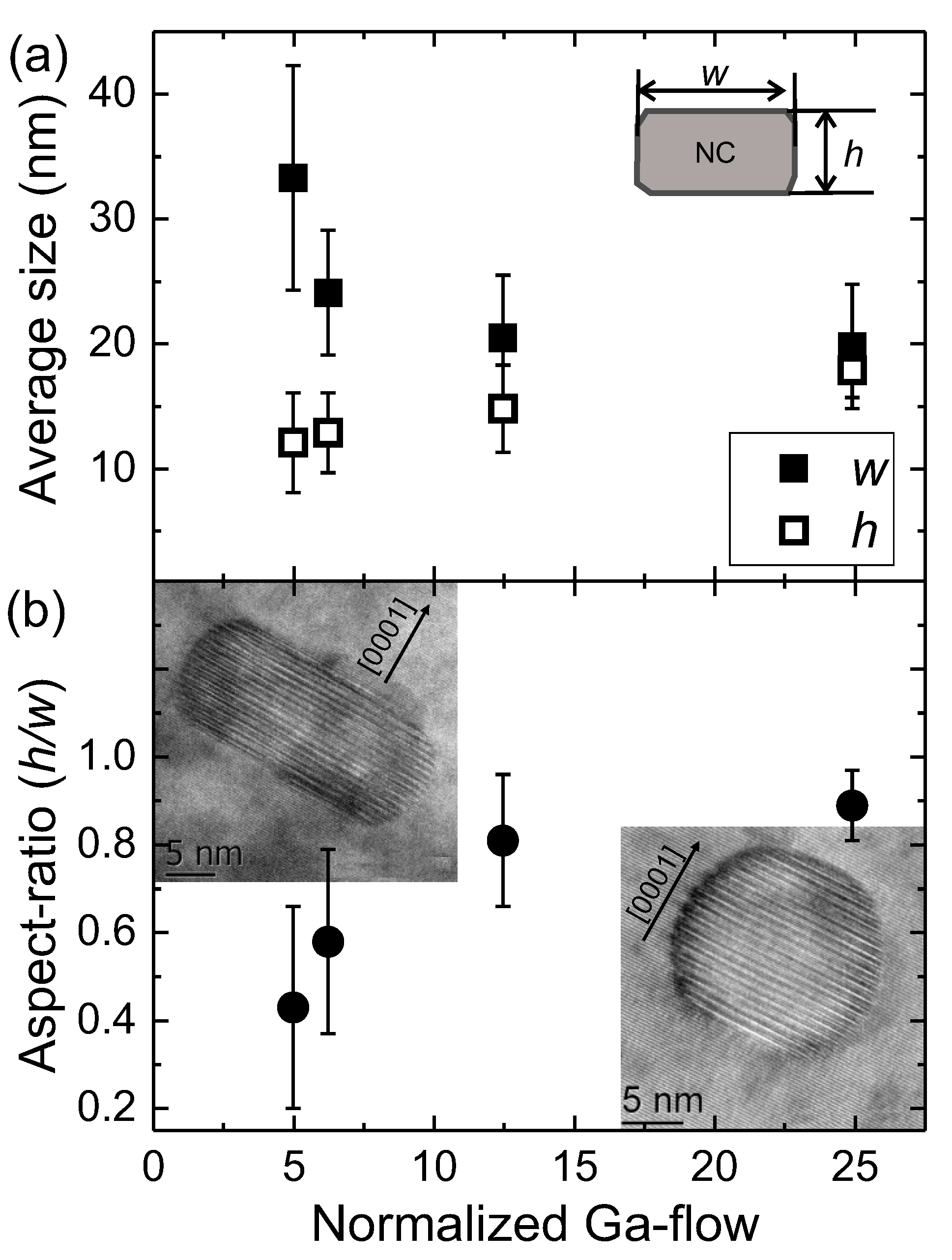
3.2. Size and Shape
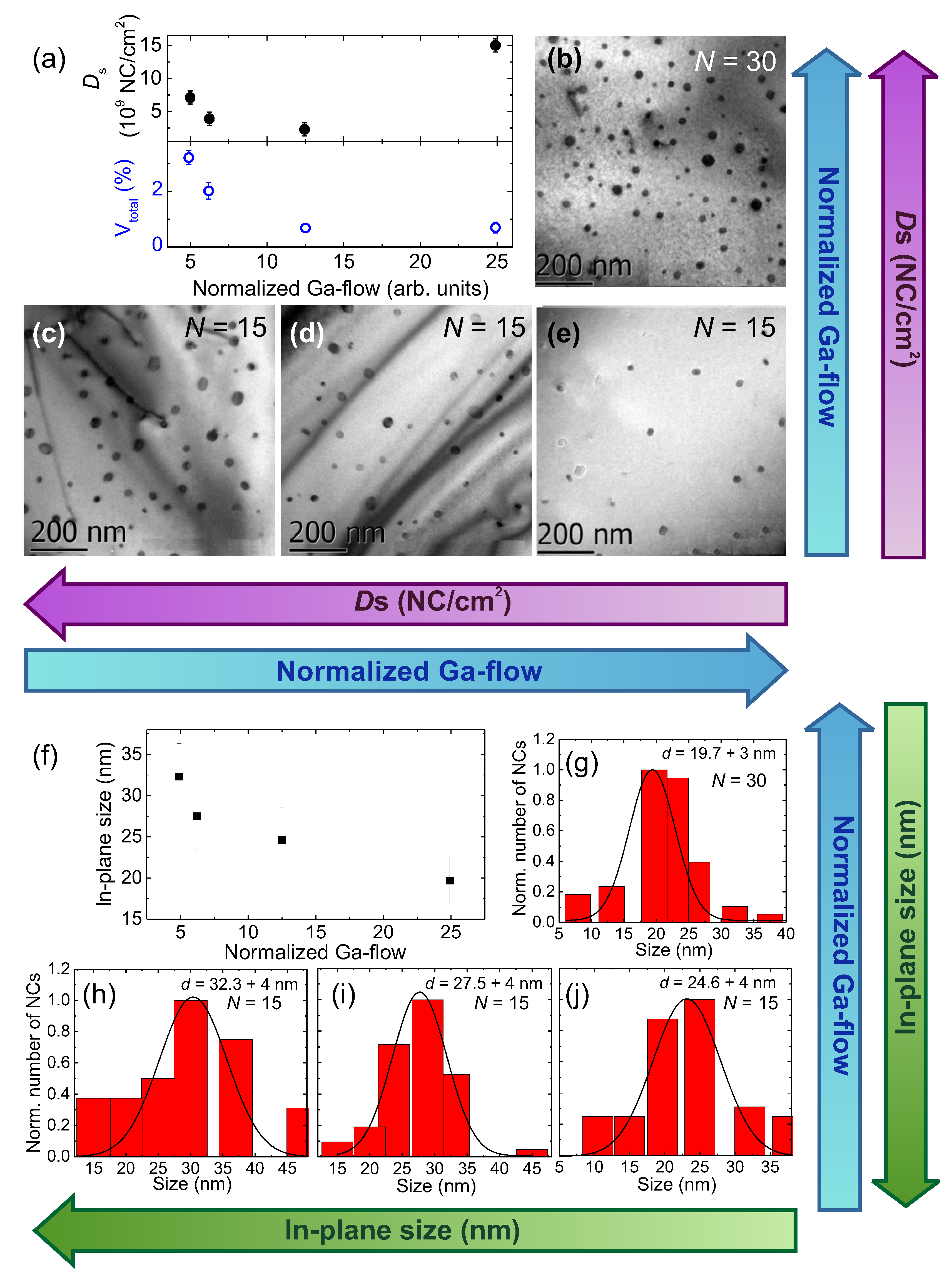
3.3. Density
4. Discussion
- Size: By varying N and in particular the Ga-flow, the overall thickness of the GaFeN layer can be adjusted, allowing to tailor the NCs size. Along the c-growth direction, the size becomes smaller with decreasing Ga-flow, and does not overcome—in the range of the considered growth conditions—the maximum of 20 nm, independently of the GaFeN layer thickness. In contrast, the in-plane diameter of the NCs increases when lowering the Ga-flow and can reach values as large as 70 nm.
- Shape: The modulation in the size of the NCs along either the in-plane or the growth direction affects the NC aspect-ratio, leading to changes in the NC shape from oblate-spheroids with aspect-ratios above 0.8 to disc-shaped NCs with aspect-ratios below 0.5. The higher the Ga-flow, the more homogeneous the shape distribution becomes. Previous ferromagnetic resonance (FMR) studies have shown that the shape of the nanocrystals plays a critical role in determining the values of the anisotropy tensor for each individual NC. The FMR measurements revealed a strong uniaxial out-of plane shape anisotropy attributed to the oblate-spheroid shape of the NCs [17].
- Density: The critical parameter for controlling , is the amount of Fe provided during fabrication. The richer the Fe conditions during growth, the higher the density of NCs. This is achieved either by decreasing the Ga-flow or by increasing the number of growth periods N and the flow of the CpFe source.
5. Conclusions
Author Contributions
Funding
Acknowledgments
Conflicts of Interest
References
- Dietl, T. A ten-year perspective on dilute magnetic semiconductors and oxides. Nat. Mater. 2010, 9, 965–974. [Google Scholar] [CrossRef] [PubMed]
- Dietl, T.; Sato, K.; Fukushima, T.; Bonanni, A.; Jamet, M.; Barski, A.; Kuroda, S.; Tanaka, M.; Hai, P.N.; Katayama-Yoshida, H. Spinodal nanodecomposition in semiconductors doped with transition metals. Rev. Mod. Phys. 2015, 87, 1311–1377. [Google Scholar] [CrossRef]
- Bonanni, A.; Dietl, T. A story of high-temperature ferromagnetism in semiconductors. Chem. Soc. Rev. 2010, 39, 528–539. [Google Scholar] [CrossRef] [PubMed]
- Sztenkiel, D.; Foltyn, M.; Mazur, G.; Adhikari, R.; Kosiel, K.; Gas, K.; Zgirski, M.; Kruszka, R.; Jakieła, R.; Li, T.; et al. Stretching magnetism with an electric field in a nitride semiconductor. Nat. Commun. 2016, 7, 13232. [Google Scholar] [CrossRef] [PubMed]
- Bonanni, A.; Kiecana, M.; Simbrunner, C.; Li, T.; Sawicki, M.; Wegscheider, M.; Quast, M.; Przybylinska, H.; Navarro-Quezada, A.; Jakieła, R.; et al. Paramagnetic GaN:Fe and ferromagnetic (Ga,Fe)N: The relation between structural, electronic and magnetic properties. Phys. Rev. B 2007, 75, 125210. [Google Scholar] [CrossRef]
- Li, T.; Simbrunner, C.; Navarro-Quezada, A.; Wegscheider, M.; Quast, M.; Litvinov, D.; Gerthsen, D.; Bonanni, A. Phase-dependent distribution of Fe-rich nanocrystals in MOVPE-grown (Ga,Fe)N. J. Cryst. Growth 2008, 310, 3294–3298. [Google Scholar] [CrossRef]
- Navarro-Quezada, A.; Stefanowicz, W.; Li, T.; Faina, B.; Rovezzi, M.; Lechner, R.; Devillers, T.; d’Acapito, F.; Bauer, G.; Sawicki, M.; et al. Embedded magnetic phases in (Ga,Fe)N: The key role of growth temperature. Phys. Rev. B 2010, 81, 205206. [Google Scholar] [CrossRef]
- Navarro-Quezada, A.; Devillers, T.; Li, T.; Bonanni, A. Planar arrays of magnetic nanocrystals embedded in GaN. Appl. Phys. Lett. 2012, 101, 081911. [Google Scholar] [CrossRef][Green Version]
- Coey, J.; Smith, P. Magnetic Nitrides. J. Magn. Magn. Mater. 1999, 200, 405–424. [Google Scholar] [CrossRef]
- Jeff, R.; Yun, M.; Ramalingam, B.; Lee, B.; Misra, V.; Triplett, G.; Gangopadhyay, S. Charge storage characteristics of ultra-small Pt nanoparticle embedded GaAs based non-volatile memory. Appl. Phys. Lett. 2011, 99, 072104. [Google Scholar] [CrossRef]
- Li, F.; Cho, S.H.; Son, D.I.; Park, K.H.; Kim, T.W. Multilevel nonvolatile memory effect in hybrid devices containing CdSe/ZnS nanoparticle double arrays embedded in the C60 matrices. Appl. Phys. Lett. 2008, 92, 102110. [Google Scholar] [CrossRef]
- Chang, T.C.; Jian, F.Y.; Chen, S.C.; Tsai, Y.T. Developments in nanocrystal memory. Mater. Today 2011, 14, 608–615. [Google Scholar] [CrossRef]
- Tsunoda, M.; Takahashi, H.; Kokado, S.; Komasaki, Y.; Sakuma, A.; Takahashi, M. Anomalous Anisotropic Magnetoresistance in Pseudo-Crystal Fe4N Films. Appl. Phys. Express 2010, 3, 113003. [Google Scholar] [CrossRef]
- Matar, S.; Demazeau, G.; Siberchicot, B. Magnetic particles derived from iron nitride. IEEE Trans. Magn. 1990, 26, 60–62. [Google Scholar] [CrossRef]
- Rovezzi, M.; d’Acapito, F.; Navarro-Quezada, A.; Faina, B.; Li, T.; Bonanni, A.; Filippone, F.; Bonapasta, A.; Dietl, T. Local structure of (Ga,Fe)N and (Ga,Fe)N:Si investigated by X-ray absorption fine structure spectroscopy. Phys. Rev. B 2009, 79, 195209. [Google Scholar] [CrossRef]
- Navarro-Quezada, A.; Swacki, N.G.; Stefanowicz, W.; Li, T.; Grois, A.; Devillers, T.; Rovezzi, M.; Jakieła, R.; Faina, B.; Majewski, J.; et al. Fe-Mg interplay and the effect of deposition mode in (Ga,Fe)N doped with Mg. Phys. Rev. B 2011, 84, 155321. [Google Scholar] [CrossRef]
- Grois, A.; Devillers, T.; Li, T.; Bonanni, A. Planar array of self-assembled GaxFe4-xN nanocrystals in GaN: Magnetic anisotropy determined via ferromagnetic resonance. Nanotechnology 2014, 25, 395704. [Google Scholar] [CrossRef] [PubMed]
- Navarro-Quezada, A.; Aiglinger, M.; Gas, K.; Matzer, M.; Faina, B.; Adhikari, R.; Sawicki, M.; Bonanni, A. Magnetotransport in phase-separated (Ga,Fe)N with g-GayFe4−yN nanocrystals. arXiv, 2018; arXiv:1809.08894. [Google Scholar]
- Bianco, L.D.; Spizzo, F.; Li, T.; Adhikari, R.; Bonanni, A. Influence of Mn co-doping on the magnetic properties of planar arrays of GaxFe4−xN nanocrystals in a GaN matrix. Phys. Rev. B. 2016, 94, 085205. [Google Scholar] [CrossRef]
- Simbrunner, C.; Sitter, H.; Bonanni, A. Fourier analysis applied on in situ laser reflectometry during III-nitride metal organic chemical vapor deposition growth. J. Appl. Phys. 2007, 101, 093501. [Google Scholar] [CrossRef]
- Patterson, A. The Scherrer Formula for X-ray Particle Size Determination. Phys. Rev. 1939, 56, 978. [Google Scholar] [CrossRef]
- Sawicki, M.; Stefanowicz, W.; Ney, A. Sensitive SQUID magnetometry for studying nanomagnetism. Semicond. Sci. Technol. 2011, 26, 064006. [Google Scholar] [CrossRef]
- Gas, K.; Sawicki, M. A practical solution for high-precision and high-sensitivity magnetometry in nanomagnetism and material science. arXiv, 2018; arXiv:1809.02346. [Google Scholar]
- Houeben, A.; Burghaus, J.; Dronskowski, R. The Ternary Nitrides GaFe3N and AlFe3N: Improved Synthesis and Magnetic Properties. Chem. Mater. 2009, 21, 4332–4338. [Google Scholar] [CrossRef]
- Burghaus, J.; Sougrati, M.; Moechel, A.; Houben, A.; Hermann, R.P.; Dronskowski, R. Local ordering and magnetism in Ga0.9Fe3.1N. J. Solid State Chem. 2011, 184, 2315–2321. [Google Scholar] [CrossRef]
- Kleibert, A.; Balan, A.; Yanes, R.; Derlet, P.M.; Vaz, C.A.F.; Timm, M.; Rodríguez, A.F.; Béché, A.; Verbeeck, J.; Dhaka, R.S.; et al. Direct observation of enhanced magnetism in individual size- and shape-selected 3d transition metal nanoparticles. Phys. Rev. B 2017, 95, 195404. [Google Scholar] [CrossRef]


| Sample | TMGa (sccm) | CpFe (sccm) | NH (sccm) | N | (s) | ± 5 (nm) | Normalized Ga-Flow |
|---|---|---|---|---|---|---|---|
| S1544 | 5.0 | 450 | 800 | 30 | 10 | 66 | 24.9 |
| S1547 | 5.0 | 450 | 800 | 15 | 10 | 46 | 12.5 |
| S1559 | 2.5 | 450 | 800 | 15 | 10 | 40 | 6.2 |
| S1656 | 2.0 | 450 | 800 | 15 | 10 | 33 | 4.9 |
| Normalized | h | h | w | Aspect-Ratio | |
|---|---|---|---|---|---|
| Ga-Flow | (nm) | (nm) | (nm) | () | ( NC/cm) |
| 24.9 | 16.5 ± 2.0 | 17.9 ± 2.2 | 19.8 ± 3.0 | 0.89 ± 0.08 | 15.0 |
| 12.5 | 14.8 ± 2.0 | 14.5 ± 3.2 | 20.5 ± 5.0 | 0.81 ± 0.15 | 2.3 |
| 6.2 | 12.4 ± 2.0 | 12.9 ± 3.5 | 24.1 ± 5.0 | 0.58 ± 0.21 | 3.9 |
| 4.9 | 10.8 ± 2.0 | 12.1 ± 4.0 | 33.4 ± 9.0 | 0.43 ± 0.23 | 7.1 |
| Fabrication Parameter | Adjusts |
|---|---|
| Growth period | Layer thickness, NCs sheet density, size and aspect-ratio |
| TMGa source flow | Layer thickness, NCs structure, size, aspect-ratio, lattice parameter, |
| Ga incorporation into the NC [8] | |
| CpFe source flow | NCs sheet density |
© 2019 by the authors. Licensee MDPI, Basel, Switzerland. This article is an open access article distributed under the terms and conditions of the Creative Commons Attribution (CC BY) license (http://creativecommons.org/licenses/by/4.0/).
Share and Cite
Navarro-Quezada, A.; Devillers, T.; Li, T.; Bonanni, A. Tuning the Size, Shape and Density of γ′-GayFe4−yN Nanocrystals Embedded in GaN. Crystals 2019, 9, 50. https://doi.org/10.3390/cryst9010050
Navarro-Quezada A, Devillers T, Li T, Bonanni A. Tuning the Size, Shape and Density of γ′-GayFe4−yN Nanocrystals Embedded in GaN. Crystals. 2019; 9(1):50. https://doi.org/10.3390/cryst9010050
Chicago/Turabian StyleNavarro-Quezada, Andrea, Thibaut Devillers, Tian Li, and Alberta Bonanni. 2019. "Tuning the Size, Shape and Density of γ′-GayFe4−yN Nanocrystals Embedded in GaN" Crystals 9, no. 1: 50. https://doi.org/10.3390/cryst9010050
APA StyleNavarro-Quezada, A., Devillers, T., Li, T., & Bonanni, A. (2019). Tuning the Size, Shape and Density of γ′-GayFe4−yN Nanocrystals Embedded in GaN. Crystals, 9(1), 50. https://doi.org/10.3390/cryst9010050