Abstract
Cu2ZnSnSe4 (CZTSe) thin films were prepared by a two-step process with the electrodeposition of a Cu/Zn metallic stack precursor followed by a reactive anneal under a Se + Sn containing atmosphere. We investigate the effect of the Sex and SnSex (x = 1,2) partial pressures and annealing temperature on the morphological, structural, and elemental distribution of the CZTSe thin films. Line scanning energy dispersive spectroscopy (EDS) measurements show the presence of a Zn-rich secondary phase at the back-absorber region of the CZTSe thin films processed with higher SnSex partial pressure and lower annealing temperatures. The Zn-rich phase can be reduced by lowering the SnSex partial pressure and by increasing the annealing temperature. A very thin MoSe2 film between the CZTSe and Mo interface is confirmed by X-ray diffraction (XRD) and grazing incidence X-ray diffraction (GIXRD) measurements. These measurements indicate a strong dependence of these process variations in secondary phase formation and accumulation. A possible reaction mechanism of CZTSe thin films was presented. In a preliminary optimization of both the SnSex partial pressure and the reactive annealing process, a solar cell with 7.26% efficiency has been fabricated.
1. Introduction
Earth-abundant and non-toxic light absorber materials, such as Cu2ZnSn(SxSe1−x)4 (CZTSSe), are an attractive candidate for thin film solar cells to meet terawatt scale production as they have an adjustable bandgap between 1.0 eV and 1.5 eV and a theoretical efficiency of above 30% [1]. Nevertheless, these materials are still at an incipient state of development, with a maximum device efficiency of 11.6% [2] and 12.6% [3] for Cu2ZnSnSe4 (CZTSe) and CZTSSe, respectively, at the laboratory scale. Their values are still far from the record cell efficiency of above 21% for Cu(In,Ga)Se2 [4] and CdTe [5]. Because of the thermodynamic stability of CZTS(e) thin films [6] and the volatility of tin selenide (SnSex ) [7], a two-step process was generally used to prepare CZTSe thin films [2,3,7,8,9,10,11,12,13]. A precursor with all or part of the CZTS(e) components was prepared first by either a vacuum or non-vacuum method and was then treated by subsequent thermal annealing to improve the crystallinity. High pressure inert gas and Se partial pressure has been applied to ensure the surface stability at the expense of excessive Se diffuse through CZTSe thin films, which react with Mo to generate thick MoSe2 films [14]. Thick MoSe2 films seem thermodynamically inevitable when considering the high Se partial pressure or high temperature [15,16]. The compactness of the precursor [8] and the annealing process must be carefully designed and controlled [10,11]. In fact, the stability of CZTSe thin films is mainly decided by the chemical equilibrium [6,17]:
Cu2ZnSnS(e)4 ←→ Cu2Se + ZnSe + SnS(e)(g) + 1/2S(e)2(g)
Therefore, the decomposition reaction can be reduced to some extent with high Se partial pressure, especially when accompanied by high inert gas pressure. However, CZTS(e) thin films were also stable when SnS(e) and S(e) coexisted in the annealing atmosphere which has been confirmed by experiments [6]. Low Se pressure annealing processes were fairly effective to avoid thick MoSe2 films. However, most published works which adopt low Se pressure, mainly investigate the feasibility of this method [12,17]. Therefore, the solar cell efficiency turns out to be lower than that prepared with high Se partial pressure. SnSex and Se are often adopted in low pressure processes, and then the Sn is introduced through the gas phase. Moreover, the surface morphology of Sn metal in the CuZnSn precursor prepared by electrodeposition [18] or physical vapor deposition [12,19] has been studied and was shown to have a significant effect on the absorber properties. We will investigate whether a precursor of only CuZn metal can be an alternative choice for preparing high quality Cu2ZnSnSe4 thin films [12,17,19].
In this work, we present a systematic study of Cu2ZnSnSe4 thin films prepared by a two-stage process as a function of SnSex (x = 1, 2) partial pressure and reactive annealing temperature. We demonstrate the importance of accurate control of both partial pressure and reactive annealing temperature, which are significant determining factors for elemental diffusion and distribution. A preliminary reaction analysis was also proposed based on the experimental results and literature data. We believe the formation of CZTSe thin films involves several sequential steps and the control step is a solid-state reaction:
Cu2SnSe3 + ZnSe←→Cu2ZnSnSe4
The optimization of experimental conditions was obtained from the experimental results. We have achieved a maximum cell efficiency of 7.26% by using a relatively low pressure at about 580 °C and identified the formation mechanisms of Cu2ZnSnSe4 thin films.
2. Materials and Methods
The metal stacks of copper and zinc with the ratio of Cu/Zn of 1.6 were electrodeposited on a molybdenum layer by the constant current method using a two-electrode system at room temperature. A 4 cm2 × 4 cm2 piece of soda-lime glass on which a 1200 nm-thick double Mo layer was deposited by DC–magnetron sputtering was used as the cathode in the electrodeposition process. Copper was electrodeposited from a solution that was freshly prepared and contained 187.5 g/L of CuSO4·5H2O and 75 g/L of H2SO4. The solution of zinc was prepared in-house using 0.2 M zinc vitriol that was dissolved in 0.5 M methane sulfuric acid [11]. The pH of the solution was adjusted to 2.2 by adding sodium hydroxide. The copper and zinc layers were electrodeposited using direct current with current densities of 50 mA/cm2 and 20 mA/cm2, respectively. The typical deposition time was about 15 seconds. Samples of the metallic precursors (4 cm2 × 4 cm2 in area) were reactively annealed in a laboratory-made furnace capable of working in vacuum (1 × 10⁻⁴ Pa) or an inert gas (Ar) atmosphere [13]. The sample temperature, Sn temperature and the Se temperature are controlled individually. The elements Sn and Se are placed in the selenization furnace, under heating. Se evaporates into the selenization furnace and reacts with Sn to form Sn–Se binary phases, which evaporate easily due to a high saturated vapor pressure. The Se and SnSex partial pressures are controlled by three parameters: the Sn and Se temperature, and the total pressure.
The electrodeposited metal stacks were annealed at 300 °C in inert gas at 1000 Pa for 30 min. Subsequently, the Se and Sn were heated to 270 °C and 300 °C respectively, then the tube was purged with inert gas to 1 × 10⁻³ Pa and the valve was closed. These samples were followed by different selenization processes. Two sets of experiments are listed in Table 1. The parameters of the first set of experiments are: total pressure of 15 Pa with Sn temperature of 550 °C, named as A1; total pressure of 15 Pa with Sn temperature of 520 °C, named A2; and total pressure of 25 Pa with Sn temperature of 520 °C, named A3. The substrate temperature was kept at 570 °C and the Se temperature was kept at 270 °C. The total pressure was adjusted by the valve of the vacuum pump manually with accuracy of ± 1 Pa. The parameters of the second set of experiments are: sample temperatures of 570 °C, 600 °C and 630 °C, named as a1, a2 and a3, respectively; tin source temperature of 550 °C in a sealed vacuum with maximum total pressure of about 40 Pa.

Table 1.
Parameters of the experiments.
A standard procedure was applied to fabricate solar cells based on the CZTSe thin film without an etching process. First, a 50 nm thick CdS was deposited using chemical bath deposition. Next, 50 nm i-ZnO and 450 nm Al-ZnO were deposited by RF sputtering. Finally, a 50 nm Ni/2 μm Al metal grid was deposited on top of the device via electron-beam evaporation through a metal mask to create a metallic grid pattern. The active area of the CZTSe solar cell was 0.358 cm2.
The structures of the selenized samples were characterized using a Philips X-pert Pro diffractometer (PANalytical Ltd., EA Almelo, the Netherlands) with Cu radiation and a Renishaw Invia Raman spectroscope (Renishaw Ltd., Gloucestershire UK) The excitation wavelength of the Raman was 514 nm. The penetration depth of this laser is around 100 nm into the absorber. The composition of the CZTSe thin film was measured using a Magix PW2403 X-ray fluorescent spectrometer (XRF, (PW2403 (PANalytical Ltd., EA Almelo, the Netherlands)) with a Rh-anode, which was calibrated by inductively coupled plasma spectroscopy (ICP, PANalytical Ltd., EA Almelo, the Netherlands). Surface and cross-sectional images were taken using a scanning electron microscope (SEM) (JEOL JSM-6700, (JEOL Ltd., Akishima-shi, Japan)). The depth profiles of the elements were obtained by line scanning energy dispersive spectroscopy (EDS). Phase identity and determination were made by Raman spectroscopy (Renishaw + Nanonics). Current–voltage (J–V) measurements of CZTSe solar cells were made under illumination by a standard AM1.5 spectrum of 1000 W/m2 at room temperature with a constant light solar simulator, which was calibrated using a standard mono-crystalline Si solar cell.
3. Results
As shown in Figure 1, depth distribution of elements in CuZn precursors was measured by line scanning energy dispersive spectroscopy (EDS) along the depth direction to estimate the effect of thermal treatment on the elemental distribution (Figure 1a,b), and the XRD pattern was used to analyze the phase transition (Figure 1c). Three peaks were observed in Figure 1a, corresponding to the elements Mo, Cu and Zn from the bottom to the surface in the Mo/Cu/Zn stacked structure, fairly consistent with the electrodeposition sequence. The overlap of Cu and Zn signals in Figure 1b, obviously in contrast to Figure 1a, reveals a more uniform distribution of CuZn after annealing. The CuZn alloy was the main phase of the electrodeposited layer in Figure 1c (black line), corresponding to the CuZn/Mo stacked structure. After thermal treatment, the Cu0.64Zn0.36 brass phase is the main phase along with some minor Cu and Zn phases. Two unknown peaks at 35.8° and 43.97° are labeled as “*”, which could be copper oxide phases. These oxides may come from the electrodeposition process. The copper has an obvious volume variation in the process of selenization, owing to the great disparities in the volume of Cu2Se and CuSe2 per copper atom [20]. The copper distribution at the bottom will inevitably create pin holes at the back-contact interface during the reactive annealing, which is detrimental to the adhesion between the absorber layer and the molybdenum substrate. Furthermore, elemental distribution has great influence on the selenization reaction process as well as the quality of absorber layer, which lead to diverse device performance [9]. We have done many experiments to selenize the Mo/Cu/Zn metal precursor directly (without annealing to form a metal alloy) in an Se + SnSe atmosphere for preparing CZTSe thin films. We found that the adhesion between the CZTSe thin film and the Mo layer was a big problem. Therefore, the formation of a CuZn alloy was essential for the follow-up selenization experiments.
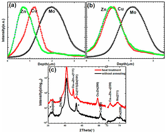
Figure 1.
Line scanning energy dispersive spectroscopy (EDS) profiles of the electroplated CuZn precursors (a) before and (b) after thermal treatment from EDS measurement. X-ray diffraction (XRD) patterns of the electrodeposited CuZn precursors (c) before and after thermal treatment.
XRD patterns of the electrodeposited CZTSe absorber layers are shown in Figure 2. The CZTSe phases are identified for all samples [21]. All samples have peaks at 17.44°, 22.05°, 42.8°, 63.83°, and 68° and those labeled as “*”. The strongest CZTSe peak is (112), in agreement with other literature data [21]. All samples except A3 have peaks at 24.5°, 29.2°, and 43.8°, which correspond to Cu2Sex (or Cu2–x Se) phases according to (ICCD#00-053-0523, ICCD#00-026-0557 and ICCD#00-027-1131). This indicates that sample A3 was more consistent with pure CZTSe phases. Binary secondary phases of CuxSe and SnSe were not easily observable because of the similarity of their crystal structures. No MoSex related diffraction peaks are observed as expected because of the low Se partial pressure employed in this work.
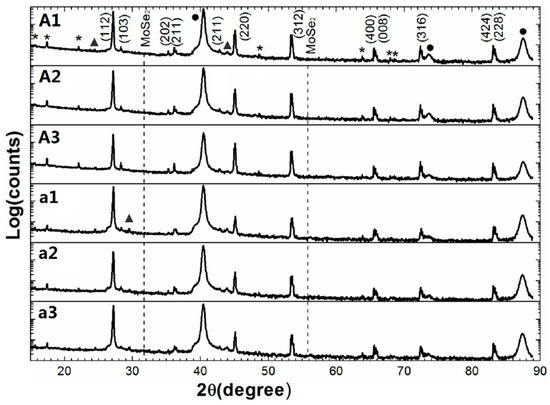
Figure 2.
XRD patterns of the A1–A3 and a1–a3 samples selenized in different selenium conditions. Mo peaks are labeled as “●”, Cu2Sex peaks are labeled as “▲” and Cu2ZnSnSe4 (CZTSe) peaks are labeled as “*”.
To further confirm the minor MoSe2 phase at the CZTSe and Mo interface, grazing incidence X-ray diffraction (GIXRD) was carried out on one of the samples with most of the CZTSe film mechanically stripped off from the sample, as shown in Figure 3. Only CZTSe and Mo related diffraction peaks was present and no MoSe2 related phase was observed (MoSe2 with a main diffraction peak at 2θ = 31.7° and 55.8° according to ICCD#00-029-0914), which is consistent with the XRD measurement in Figure 2.
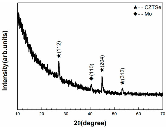
Figure 3.
Grazing incidence X-ray diffraction (GIXRD) pattern of the sample with most of the CZTSe film having been mechanically stripped off.
Because of the similarity in diffraction patterns, XRD cannot unambiguously identify ZnSe, Cu2SnSe3 and CZTSe, and therefore it is necessary to use other characterization techniques to identify CZTSe such as Raman spectroscopy. As shown in Figure 4, the Raman peak positions at 195 cm−1,173 cm−1 and 234 cm−1 were identified as the main peaks of the CZTSe phase. The weak peak at 249 cm−1 corresponds to ZnSe phases [12], Cu2SnSe3 [22] or disordered CZTSe phases [23]. This is confirmed to be Cu2SnSe3 according to the Zn-poor surface confirmed by the follow-up line scanning EDS analysis of CZTSe thin films. For samples A1−A3, the intensity at 249 cm−1 decreased with lower SnSex partial pressure, revealing that Cu2SnSe3 at the surface region is reduced. For samples a1-a3, sample a1 and a2 have an obvious peak intensity at 249 cm−1, and a2 has a weak peak intensity here, revealing that annealing at 600 °C in a sealing atmosphere results in less Cu2SnSe3 phases. This will be discussed in the following sections.
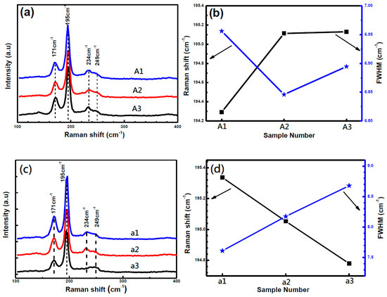
Figure 4.
Raman spectroscopy of the A1–A3 and a1–a3 samples selenized with different selenization conditions.
The Raman spectrum with Lorenzian fitting was carried out and the peak position, peak intensity and full width half maximum (FWHM) data were analyzed. As listed in Table 2, peak position and FWHM changed from 194.29 cm−1 to 195.11 cm−1 and from 6.96 cm−1 to 6.85cm−1, respectively, for samples A1 and A2 with lower SnSex partial pressure and higher Se partial pressure. However, it changed little with further adjustment to the Se and SnSe partial pressure for A2 and A3. This indicates that higher Se and lower SnSe partial pressure were preferred for the formation of pure CZTSe phases. However, excessive SnSex would cause secondary phases. Annealing temperature has an obvious influence on the Raman spectrum parameters. The peak position decreases and the FWHM increases with increasing annealing temperature from 570 °C to 630 °C. The broad CZTSe peaks are observed and Cu2SnSe3 was confirmed to be present at the surface layer. More information could be obtained from the Raman spectra, like the order–disorder character and the degree of crystallization. The broadening peak may arise from a high defect density and local compositional fluctuations. The local disorder in the cation sub-lattice could also be a reason for the peak shoulder [23,24]. A higher peak position accompanied with lower FWHM values corresponds to higher crystallization quality [12].
Table 2.
Raman peak position, full width half maximum (FWHM) and peak intensity calculated by Raman spectra with Lorenzian fitting.
To further analyze the effect of annealing condition on the morphology, secondary phases and elemental distribution, scanning electron microscopy (SEM) with line scanning EDS was applied. In order to facilitate the discussion, gas phase partial pressure analysis in the selenium atmosphere will be discussed first. It is well known that only SnSe2 and SnSe phases were verified experimentally in the Sn–Se system, and no Sn2Se3 was found [7]. The saturated vapor pressure (units in Pa) of Se, SnSe and SnSe2 at the temperature adopted in this work are listed in Table 3. The statured vapor pressure of SnSe2 is two order of magnitudes higher than that of SnSe; therefore, SnSe2 was considered as the main Sn-containing vapor gas in this work and the SnSe phase was neglected.
Table 3.
The saturated vapor pressure (units in Pa) of SnSe and SnSe2 [7,13,25].
At the beginning of the selenization process, the annealing furnace was quickly injected with Se vapor and the Sn-containing vapor phase was negligible because the saturated vapor pressure of Sn was low [25]. Subsequently, Sn reacts with Se to generate SnSe2, and SnSe2 evaporates into the annealing furnace and reacts with the precursor. The SnSe2 partial pressure was affected by the reaction rate of Se with Sn, i.e., Sn temperature and the Se partial pressure. The analysis of partial pressure is listed in Table 4 based on the data in table and the experimental conditions. Figure 5 shows the cross-sectional and surface SEM micrographs of samples A1–A3. Large CZTSe grain with a smooth and compact surface was observed in Figure 5a,d, accompanied by large holes and Zn-rich secondary phases at the CZTSe/Mo interface (which will be confirmed by EDS and shown herein later). The holes and Zn-rich secondary phases between CZTSe and Mo diminished with increasing Se partial pressure and decreasing SnSex partial pressure, as shown in Figure 5b. The surface roughness increased, and grain size decreased in Figure 5b,e. With further lower SnSex partial pressures and higher Sex partial pressures, isolated hill-shaped grains were obtained and covered the whole film. Almost no holes and secondary phases existed at the interface in Figure 5c,f. Unsurprisingly, the biggest surface roughness was observed in the trend of A1 and A2. It was obvious that with higher Sex partial pressure and lower SnSex partial pressure, the grain tends grow longitudinally through the film. In contrast, with low Se partial pressure and higher SnSe partial pressure, the grain tends to growth laterally at the surface.
Table 4.
The partial pressure (units in Pa) of Se and SnSe2.
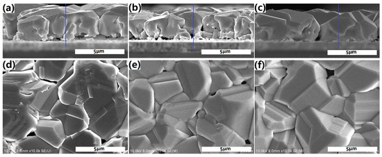
Figure 5.
Cross-sectional and surface scanning electron microscopy (SEM) micrographs of the A1–A3 and a1–a3 samples prepared under different conditions. The scanning line is indicated by a blue line in (a–c).
Figure 6 shows the line scanning EDS profiles of the samples A1–A3 (the scanning line (blue line) is indicated in Figure 5a,b,c). The SnSex partial pressures from high to low for the preparation of sample A1, A2 and A3 were sample A1, A3 and A2, respectively. Sample A1 is Zn-poor at the surface region and Sn-poor at the bottom region. However, sample A2 is Sn-poor and Zn-rich at the surface region, indicating that lower SnSex partial pressures for sample A2 can result in better Sn in-diffusion than higher SnSex partial pressures for sample A1. Lower SnSex partial pressure is beneficial to the interdiffusion of Sn and Zn for a reactive annealing Cu/Zn metallic stack precursor. It is well known that a higher total pressure can prevent the Sn loss from the surface of CZTSe thin films owing to the high saturated vapor pressure of SnSex. Therefore, properly adjusting the annealing parameter by slightly increasing SnSex partial pressure and the total pressure of sample A3 leads to more uniform element distribution than those shown for samples A1 and A2, as shown in Figure 6c.
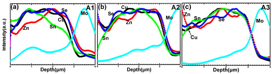
Figure 6.
Line scanning EDS profiles of samples A1–A3.
Figure 7 shows the cross-sectional and surface SEM micrographs for samples a1–a3. As shown in Figure 7a, the 500 nm-thick secondary phase for sample a1 exists at the CZTSe/Mo interface, which is confirmed to be a Zn-rich phase by the line scanning EDS profiles of sample a1. It reveals an insufficient reaction of the phases at the interface region. No secondary phase, except a few pin holes at the CZTSe/Mo interface, is observed at an annealing temperature of 600 °C, as shown in Figure 7b. It also reveals that a sufficient reaction of the phases occurred at the interface region. Secondary phases appeared with further increases of the annealing temperature to 630 °C, as shown in Figure 7c, which will be discussed later. Coherent and compact grain of the upper layer with a flat surface was observed for all three samples. The grain boundary becomes more compact and the grain size increases with increasing temperature, as shown in Figure 7d,e,f. The grain size exceeding 10 μm was obtained for sample a3.
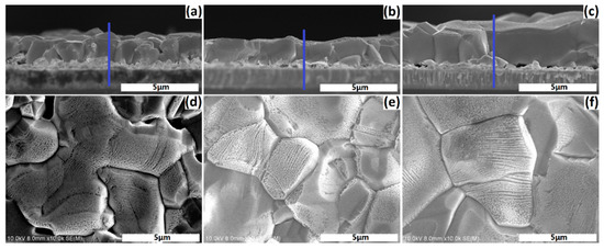
Figure 7.
Cross-sectional and surface SEM micrographs of samples a1–a3.
Figure 8 shows the line scanning EDS profiles of samples a1–a3. The elemental signal intensity variation of the surface regions of samples a1–a3 was sharper than that of samples A2 and A3. They reveal a smooth surface in samples a1–a3. Sample a1 has a Sn-rich and Zn-poor composition at the surface region and a Zn-rich composition at the bottom region. This indicates that Sn and Zn diffusion is inadequate for samples annealed at 570 °C. However, for the sample annealed at 600 °C, the Zn-rich composition at the bottom region disappears which indicates that Zn diffusion is sufficient. A Sn-rich surface region still exists, which may originate from the sealed selenization conditions with relatively higher SnSex partial pressure compared to that of samples A1–A3. When further increasing the annealing temperature to 630 °C (sample a3), a thick Zn-poor surface region and interface region reveals that it is unfavorable to form CZTSe at 630 °C.
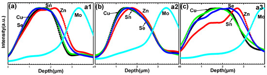
Figure 8.
Line scanning EDS profiles of samples a1–a3.
The composition of the samples is listed in Table 5. The ratio of Cu/Zn was about 1.6 for all samples. For samples A1–A3, the Zn/Sn ratio is lower and the Sn content is higher at low SnSex partial pressure, in agreement with the observation of Sn diffusion in Figure 6. For the samples a1–a3, the Zn/Sn ratio decreases and the Sn content increases with increasing annealing temperature. The Zn diffusion is more rapid for sample a2 in comparison with a1, and the higher Sn content is accessible. However, the Zn/Sn ratio for sample a3 with poor Zn diffusion is abnormal. Sample A1 and a3 have different compositions, although both of them have poor element diffusion. However, minor differences can be observed between Figure 6a and Figure 8c. Sample A1 has poor Sn and Zn diffusion, whereas sample a1 has good Sn diffusion and poor Zn diffusion.
Table 5.
Composition of sample annealing under different conditions.
As shown above, the formation process of CZTSe thin film from a CuZn precursor under Sn + Se atmosphere is affected by many factors, such as annealing temperature, Se partial pressure, SnSex partial pressure and total pressure. To verify the diffusion process, another set of experiments were carried out with annealing times of 1 min, 2 mins, 4 mins, 8 mins and 16 min, named as s1,s2, s4, s8 and s16, respectively. The cross-section SEM images and line scanning EDS profiles are shown in Figure 9. Secondary phases at the CZTSe/Mo interface and the size of voids in the film both decrease and finally disappear with an increase in annealing time. The line scanning EDS profiles of samples s1 through s16 reveal the process of elemental diffusion. At the initial stage, as shown in Figure 9f, Zn and Cu were the main elements and little Sn existed in the middle region. When increasing the annealing time, Sn diffuses to the bottom region and Zn diffuses to the surface, as shown in Figure 9f,j. For all samples, a Cu-rich surface region is observed, owing to the surface tension of liquid phase Cu2–x Se at above 570 °C.
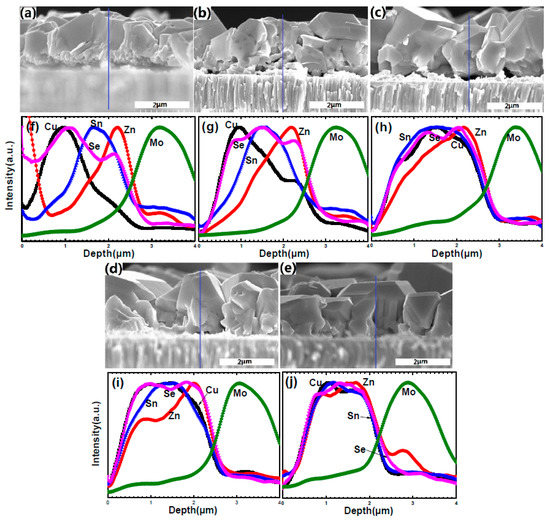
Figure 9.
Cross-section SEM images and line scanning EDS profiles of samples s1–s16.
It was reported that the formation of CZTSe thin films involves reaction (1) and (2) [19,26]. The sample temperature of the CuxZny precursor is heated to a higher temperature than 570 °C for 3 min. The main selenization reactions of the CuxZny precursor are [19,26]:
CuxZny+Sex(g)→Cu2Se+ZnSe
Cu2Se+SnSex(g)→Cu2SnSe3
Cu2SnSe3+ZnSe→Cu2ZnSnSe4
The selenization reaction process is proposed as shown in Figure 10. The reaction of CuxZny with Se has been confirmed experimentally in the literature [27] and adopted here as described in reaction (3). Sn reacts with Se to produce SnSex, and the evaporation of SnSex was feasible with temperatures higher than 400 °C [12,13]. Then, SnSex reacts with Cu2Se to produce Cu2SnSe3 as described in reaction (4). At the same time, Cu2SnSe3 is consumed by the reaction with ZnSe and generates Cu2ZnSnSe4 as described in reaction (5). The rate of reaction (4) is affected by the partial pressure of SnSex, as well as the diffusion rate of copper. A higher Sn temperature leads to higher SnSex partial pressure, and a higher annealing temperature leads to a faster copper diffusion rate. In a similar way, a higher reaction rate (5) can be obtained at higher annealing temperatures.
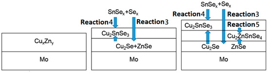
Figure 10.
The proposed selenization reaction process of CuxZny precursors.
The equilibrium between the production and the consumption of Cu2SnSe3 results in a significant effect on the morphology, crystallization and distribution of the elements. In sample A1 (high SnSex partial pressure), the production reaction of Cu2SnSe3 is in the ascendant, i.e. reaction (4) may be faster than reaction (5). Cu2SnSe3 grain grows fast and leads to a compact surface at the upper layer and Zn-rich layer at the bottom. However, in sample A3 (low SnSex partial pressure), the Cu2SnSe3 reaction is slower than that of sample 1. In addition, the overall pressure can also enhance these reactions. Reaction (4) may be slower than reaction (5), i.e., the formation of Cu2ZnSnSe4 thin films is faster than the formation of Cu2SnSe3 thin films. The large grain through the whole film is expected in this situation. With increasing annealing temperature from 570 °C to 600 °C, the consumption reaction Cu2SnSe3 is enhanced, the elemental distribution is uniform and secondary phases can be avoided. The production of Cu2SnSe3 is significantly affected by SnSex partial pressure when considering the liquid phase Cu2–xSe. However, the consumption rate is a solid-phase reaction greatly affected by temperature. Therefore, an increased annealing temperature can promote reaction (5) and avoid the secondary phases at the CZTSe/Mo interface, which is in agreement with experiment a2. With high annealing temperature, good crystallization at the upper layer is formed quickly with grain size exceeding 10 μm, which impedes the solid phase reaction (5), and therefore the Zn-rich region is left at the bottom.
The current–voltage (J–V) curves of samples A1–A3 and a1–a3 are shown in Figure S1. Table S1 lists the performance parameters of these solar cells. The highest efficiency open circuit voltage and short current density of these samples is reached with samples A2, A2, and a2, respectively. This means that the annealing parameters of the devices that perform the best may be in the range of sample temperatures from 570 °C to 600 °C, Sn temperatures from 520 °C to 550 °C and total pressures from 15 Pa to 40 Pa. The equilibrium between the production and the consumption can be obtained by carefully adjusting the experimental parameters, such as SnSex partial pressure and annealing temperature. Optimized annealing parameters were obtained based on the analysis above, and a CZTSe solar cell was fabricated at 580 °C with a Sn temperature of 550 °C and a total pressure of 30 Pa. Figure 11a,b shows the cross-sectional and surface images of the CZTSe thin films. A compact surface and columnar-like grain are observed. The current–voltage (J–V) curve of this CZTSe solar cell is shown in Figure 11c. It presents an efficiency of 7.26% with VOC = 394 mV, JSC = 32.27 mA/cm2, FF = 57.1%.
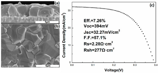
Figure 11.
(a) Cross-sectional and (b) surface SEM images of CZTSe thin films for sample annealing at optimized parameters. (c) The current–voltage (J–V) curve of the best cell at AM1.5 illumination.
4. Conclusions
The electrodeposited CZTSe thin films were prepared by a two-step process under low-pressure. The impact of the Se and SnSe partial pressures and the annealing temperature were studied. Both parameters have significant effects on the morphology, crystallization and elemental distribution of CZTSe thin films. We have shown that the equilibrium between the production and consumption of the Cu2SnSe3 phase is the critical step for the formation of high quality CZTSe thin films. We also present the effect of process parameters on the growth process and elemental distribution. Increasing the SnSex partial pressure promotes the formation of the Cu2SnSe3 phase at the upper layer and leads to a smooth and compact layer, but this is at the expense of leaving ZnSe at the bottom region. Increasing the annealing temperature from 570 °C to 600 °C leads to a reduction of the ZnSe concentration at the bottom due to the rapid reaction rate of Cu2SnSe3 with ZnSe. However, with high annealing temperatures of 630 °C, the compact grain size becomes too large, which impedes the consumption of ZnSe. The equilibrium between the production and the consumption reaction is obtained by carefully adjusting the Se and SnSe partial pressure and annealing temperatures. The best performing device has a power conversion efficiency of 7.26%. The optimized parameters are at a sample temperature of 580 °C, a Sn temperature of 550 °C and a total pressure of 30 Pa.
Supplementary Materials
The following are available online at http://www.mdpi.com/2073-4352/9/1/10/s1. Figure S1: The J-V curves of CZTSe solar cells with sample A1–A3 and a1–a3; Table S1: Solar performance parameters of CZTSe solar cells with sample A1–A3 and a1–a3.
Author Contributions
Conceptualization, L.Y. and J.A.; methodology, G.S., Q.H., Z.Z. and Y.Z.; investigation, L.Y., J.B. and S.G.; writing—original draft preparation, L.Y.; writing—review and editing, M.-J.J.; supervision, J.A., Y.S. and L.-B.C.
Funding
This research was funded by the National Natural Science Foundation of China (61674082, 61274053, 51572132), and the Tianjin Natural Science Foundation of Key Projects (16JCZDJC30700), the China Postdoctoral Science Foundation (2018M631730), and the YangFan Innovative and Entrepreneurial Research Team Project (2014YT02N037). This research was also funded by Chang Gung University, Chang Gung Memorial Hospital and the Ministry of Science and Technology, Republic of China under the Contract No. NERPD2G0251, BMRPA52 and MOST 106-2221-E-182-046.
Conflicts of Interest
The authors declare no conflict of interest.
References
- Ki, W.S.; Hillhouse, H.W. Earth-Abundant Element Photovoltaics Directly from Soluble Precursors with High Yield Using a Non-Toxic Solvent. Adv. Energy Mater. 2011, 1, 732–735. [Google Scholar] [CrossRef]
- Lee, Y.S.; Gershon, T.; Gunawan, O.; Todorov, T.K.; Gokmen, T.; Virgus, Y.; Guha, S. Cu2ZnSnSe4 Thin-Film Solar Cells by Thermal Co-evaporation with 11.6% Efficiency and Improved Minority Carrier Diffusion Length. Adv. Energy Mater. 2014, 4, 1401372. [Google Scholar]
- Wang, W.; Winkler, M.T.; Gunawan, O.; Gokmen, T.; Todorov, T.K.; Zhu, Y.; Mitzi, D.B. Characteristics of CZTSSe Thin-Film Solar Cells with 12.6% Efficiency. Adv. Energy Mater. 2014, 4, 1301465. [Google Scholar] [CrossRef]
- Jackson, P.; Hariskos, D.; Wuerz, R.; Kiowski, O.; Bauer, A.; Friedlmeier, T.M.; Powalla, M. Properties of Cu(In,Ga)Se2 solar cells with new record efficiencies up to 21.7%. Phys. Status Solidi (RRL) Rapid Res. Lett. 2015, 9, 28–31. [Google Scholar] [CrossRef]
- Green, M.A.; Emery, K.; Hishikawa, Y.; Warta, W.; Dunlop, E.D. Solar cell efficiency tables (Version 45). Prog. Photovolt. Res. Appl. 2015, 23, 1–3. [Google Scholar] [CrossRef]
- Scragg, J.J.; Ericson, T.; Kubart, T.; Edoff, M.; Platzer-Björkman, C. Chemical Insights into the Instability of Cu2ZnSnS4Films during Annealing. Chem. Mater. 2011, 23, 4625–4633. [Google Scholar] [CrossRef]
- Sharma, R.C.; Chang, Y.A. The Se-Sn (Selenium-Tin) System. Bull. Alloy Phase Diagr. 1986, 7, 68–72. [Google Scholar] [CrossRef]
- Li, J.; Zhang, Y.; Zhao, W.; Nam, D.; Cheong, H.; Wu, L.; Zhao, Z.; Sun, Y. A Temporary Barrier Effect of the Alloy Layer During Selenization: Tailoring the Thickness of MoSe2 for Efficient Cu2ZnSnSe4 Solar Cells. Adv. Energy Mater. 2015, 5, 1570048. [Google Scholar] [CrossRef]
- Jiang, F.; Ikeda, S.; Harada, T.; Matsumura, M. Pure Sulfide Cu2ZnSnS4Thin Film Solar Cells Fabricated by Preheating an Electrodeposited Metallic Stack. Adv. Energy Mater. 2013, 3, 1301381. [Google Scholar] [CrossRef]
- Jeon, J.O.; Lee, K.D.; Oh, L.S.; Seo, S.W.; Lee, D.; Kim, K.H.; Jeong, J.H.; Ko, M.J.; Kim, B.S.; Son, H.J.; et al. Highly Efficient Copper–Zinc–Tin–Selenide (CZTSe) Solar Cells by Electrodeposition. ChemSusChem 2014, 7, 1073–1077. [Google Scholar] [CrossRef]
- Ahmed, S.; Reuter, K.B.; Gunawan, O.; Guo, L.; Romankiw, L.T.; Deligianni, H. A High Efficiency Electrodeposited Cu2ZnSnS4 Solar Cell. Adv. Energy Mater. 2012, 2, 253–259. [Google Scholar] [CrossRef]
- Fairbrother, A.; Fontané, X.; Izquierdo-Roca, V.; Placidi, M.; Sylla, D.; Espindola-Rodriguez, M.; López-Mariño, S.; Pulgarín, F.A.; Vigil-Galán, O.; Pérez-Rodríguez, A.; et al. Secondary phase formation in Zn-rich Cu2ZnSnSe4-based solar cells annealed in low pressure and temperature conditions. Prog. Photovolt. Res. Appl. 2014, 22, 479–487. [Google Scholar] [CrossRef]
- Yao, L.Y.; Ao, J.P.; Jeng, M.J.; Bi, J.L.; Gao, S.S.; He, Q.; Zhou, Z.Q.; Sun, G.Z.; Sun, Y.; Chang, L.B.; et al. CZTSe solar cells prepared by electrodeposition of Cu/Sn/Zn stack layer followed by selenization at low Se pressure. Nanoscale Res. Lett. 2014, 9, 678. [Google Scholar] [CrossRef]
- Shin, B.; Bojarczuk, N.A.; Guha, S. On the kinetics of MoSe2 interfacial layer formation in chalcogen-based thin film solar cells with a molybdenum back contact. Appl. Phys. Lett. 2013, 102, 091907. [Google Scholar] [CrossRef]
- Kaupmees, L.; Altosaar, M.; Volobujeva, O.; Barvinschi, P. Study of Mo selenisation process on different Mo substrates. In Thin-Film Compound Semiconductor Photovoltaics—MRS Spring Meeting; Cambridge Univ. Press: Cambridge, UK, 2009. [Google Scholar]
- Kumar, M.; Dubey, A.; Adhikari, N.; Venkatesan, S.; Qiao, Q. Strategic review of secondary phases, defects and defect-complexes in kesterite CZTS–Se solar cells. Energy Environ. Sci. 2015, 8, 3134–3159. [Google Scholar] [CrossRef]
- Redinger, A.; Berg, D.M.; Dale, P.J.; Siebentritt, S. The consequences of kesterite equilibria for efficient solar cells. J. Am. Chem. Soc. 2011, 133, 3320–3323. [Google Scholar] [CrossRef] [PubMed]
- Scragg, J.J.; Berg, D.M.; Dale, P.J. A 3.2% efficient Kesterite device from electrodeposited stacked elemental layers. J. Electroanal. Chem. 2010, 646, 52–59. [Google Scholar] [CrossRef]
- Wibowoa, R.A.; Moeckelb, S.A.; Yoo, H.; Hetzner, C.; Hoelzing, A.; Wellmann, P.; Hock, R. Intermetallic compounds dynamic formation during annealing of stacked elemental layers and its influences on the crystallization of Cu2ZnSnSe4 films. Mater. Chem. and Phys. 2013, 142, 311–317. [Google Scholar] [CrossRef]
- Beck, M.E.; Swartzlander-Guest, A.; Matson, R.; Keane, J.; Noufi, R. CuIn(Ga)Se2-based devices via a novel absorber formation process. Sol. Energy Mater. Sol. Cells 2000, 64, 135–165. [Google Scholar] [CrossRef]
- Guo, L.; Zhu, Y.; Gunawan, O.; Gokmen, T.; Deline, V.R.; Ahmed, S.; Romankiw, L.T.; Deligianni, H. Electrodeposited Cu2ZnSnSe4thin film solar cell with 7% power conversion efficiency. Prog. Photovolt.: Res. Appl. 2014, 22, 58–68. [Google Scholar] [CrossRef]
- Ahmadi, M.; Pramana, S.S.; Batabyal, S.K.; Boothroyd, C.; Mhaisalkar, S.G.; Lam, Y.M. Synthesis of Cu2SnSe3 Nanocrystals for Solution Processable Photovoltaic Cells. Inorgan. Chem. 2013, 52, 1722–2728. [Google Scholar] [CrossRef] [PubMed]
- Rey, G.; Redinger, A.; Sendler, J.; Weiss, T.P.; Thevenin, M.; Guennou, M.; El Adib, B.; Siebentritt, S. The band gap of Cu2ZnSnSe4: Effect of order-disorder. Appl. Phys. Lett. 2014, 105, 112106. [Google Scholar] [CrossRef]
- Scragg, J.J.; Choubrac, L.; Lafond, A.; Ericson, T.; Platzer-Björkman, C. A low-temperature order-disorder transition in Cu2ZnSnS4 thin films. Appl. Phys. Lett. 2014, 104, 041911. [Google Scholar] [CrossRef]
- Yaws, C.L. Handbook of Vapor Pressure: Volume 4. Inorganic Compounds and Elements; Gulf Professional Publishing: Houston, TX, USA, 1995. [Google Scholar]
- Fella, C.M.; Uhl, A.R.; Romanyuk, Y.E.; Tiwari, A.N. Cu2ZnSnSe4 absorbers processed from solution deposited metal salt precursors under different selenization conditions. Phys. Status Solidi 2012, 209, 1043–1048. [Google Scholar] [CrossRef]
- Yoo, H.; Wibowo, R.A.; Manoharan, G.; Lechner, R.; Jost, S.; Verger, A.; Palm, J.; Hock, R. The formation mechanism of secondary phases in Cu2ZnSnSe4 absorber layer. Thin Solid Films 2015, 582, 245–248. [Google Scholar] [CrossRef]


© 2018 by the authors. Licensee MDPI, Basel, Switzerland. This article is an open access article distributed under the terms and conditions of the Creative Commons Attribution (CC BY) license (http://creativecommons.org/licenses/by/4.0/).