Investigation of the Grain Boundary Character and Dislocation Density of Different Types of High Performance Multicrystalline Silicon

Abstract
1. Introduction
- Dislocation clusters are far less abundant than in conventional material, and the clusters do not proliferate uncontrollably as growth proceeds (i.e., upwards in the ingot);
- Grain sizes are smaller than before, starting in the mm2 size, growing to cm2 towards the top. Previously, very large grains developed even at the very bottom of the ingot without grain selection, and several cm2 would be expected at the top;
- Grain boundaries have a different structure and composition than before; whereas the large majority of grain boundaries used to be coincidence site lattice (CSL) boundaries, particularly of the Σ3 type, currently a much larger proportion of random angle grain boundaries (RAGB) is present.
2. Materials and Methods
3. Results
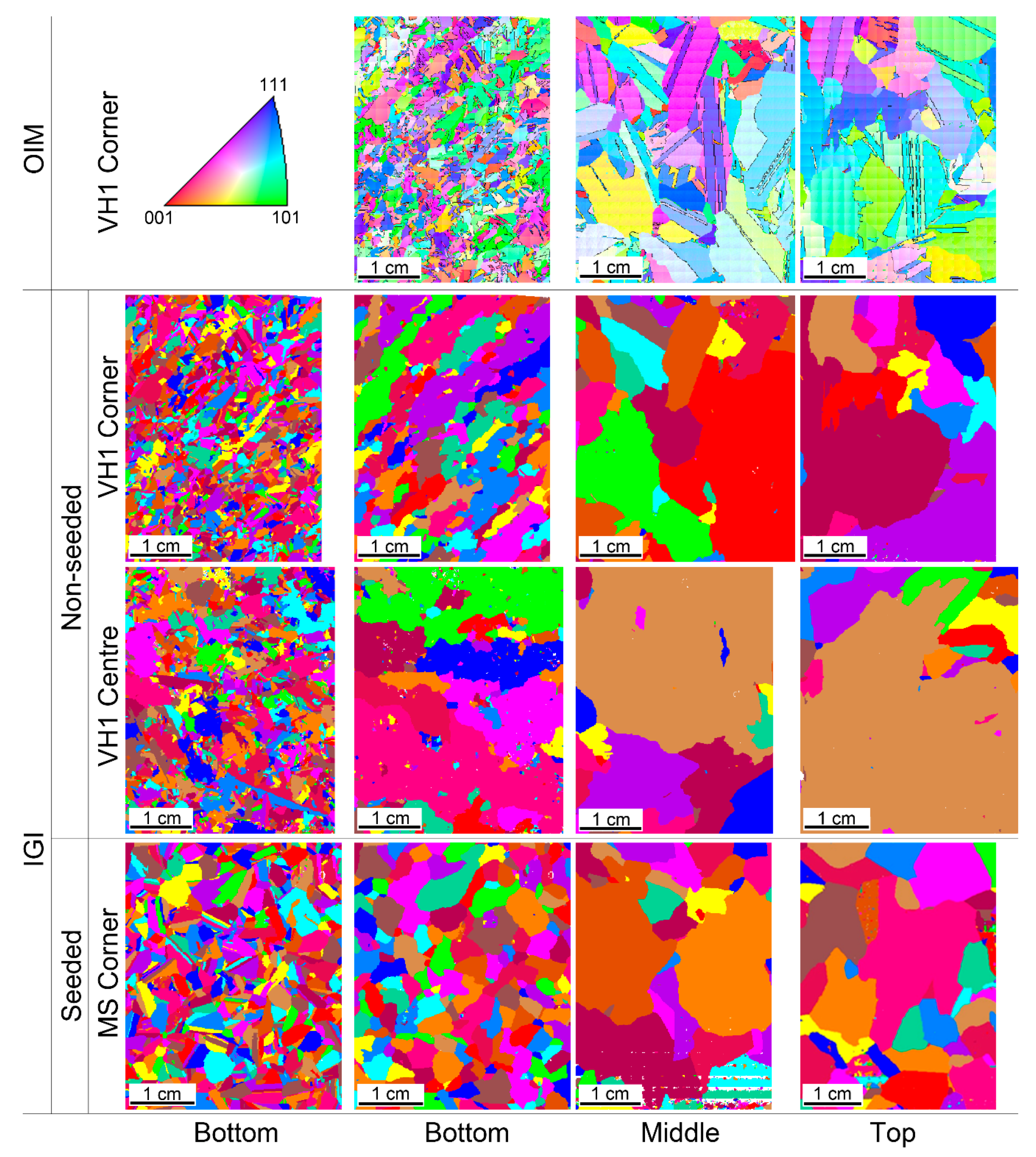
3.1. Grain Size
- The IGIs where twins are included indicate that the bottom wafers of the non-seeded ingot have an overall smaller grain size than the seeded ingot;
- This relation is reversed when twins are disregarded. This is particularly evident for the centre block;
- Further up in the ingot, the difference between seeded and non-seeded decreases; however, the grain size in the centre block is generally somewhat larger.
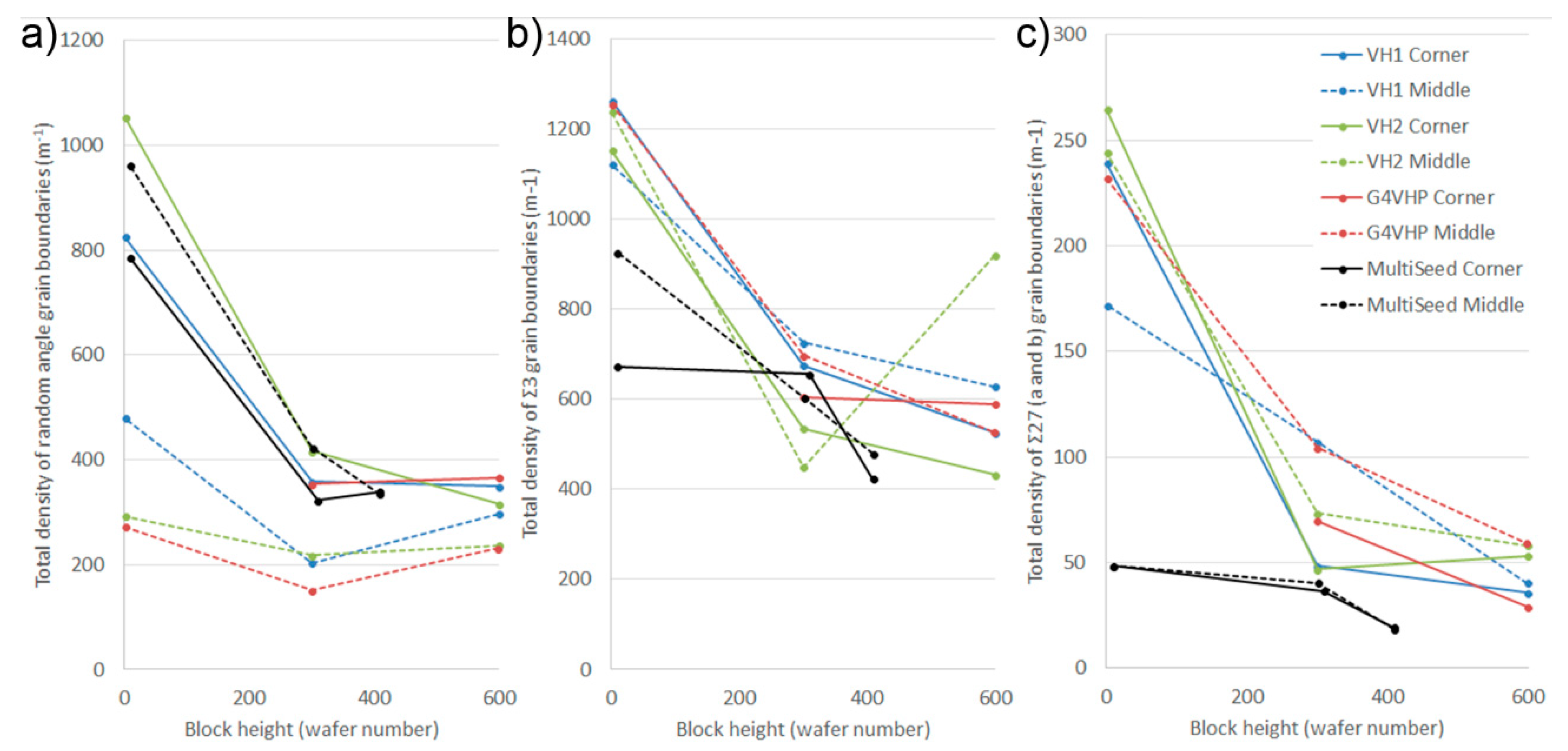
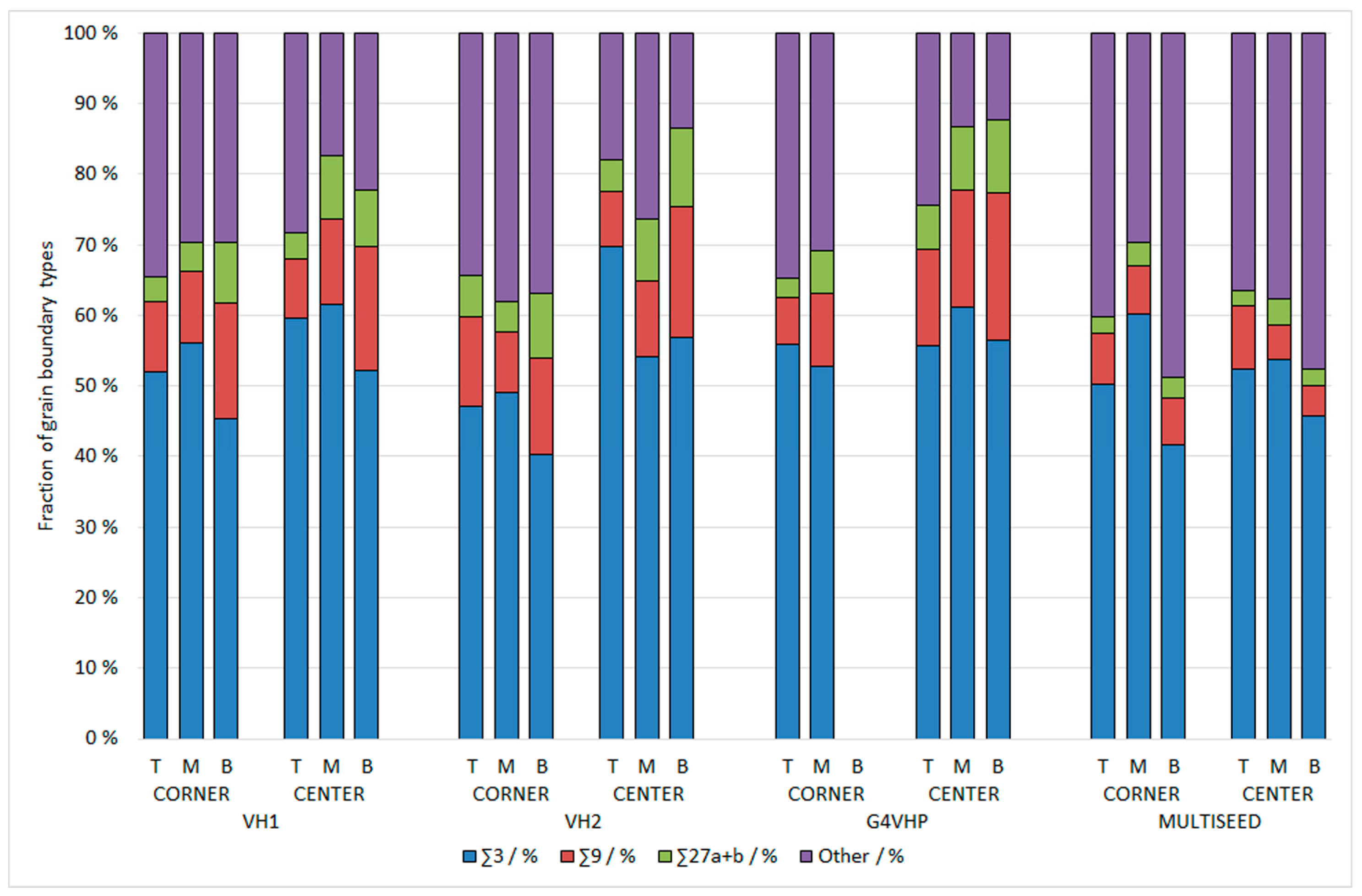
3.2. Grain Boundaries
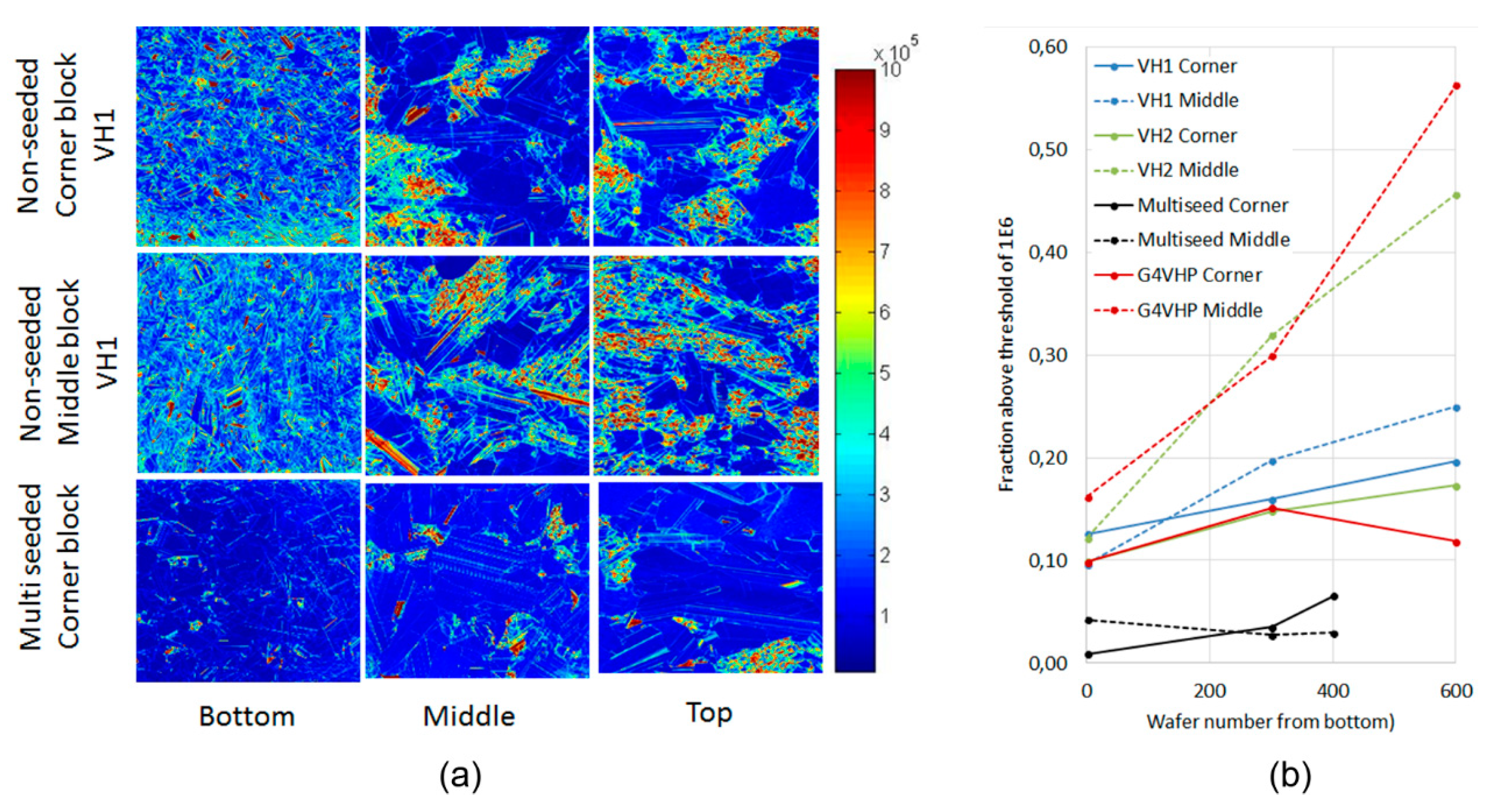
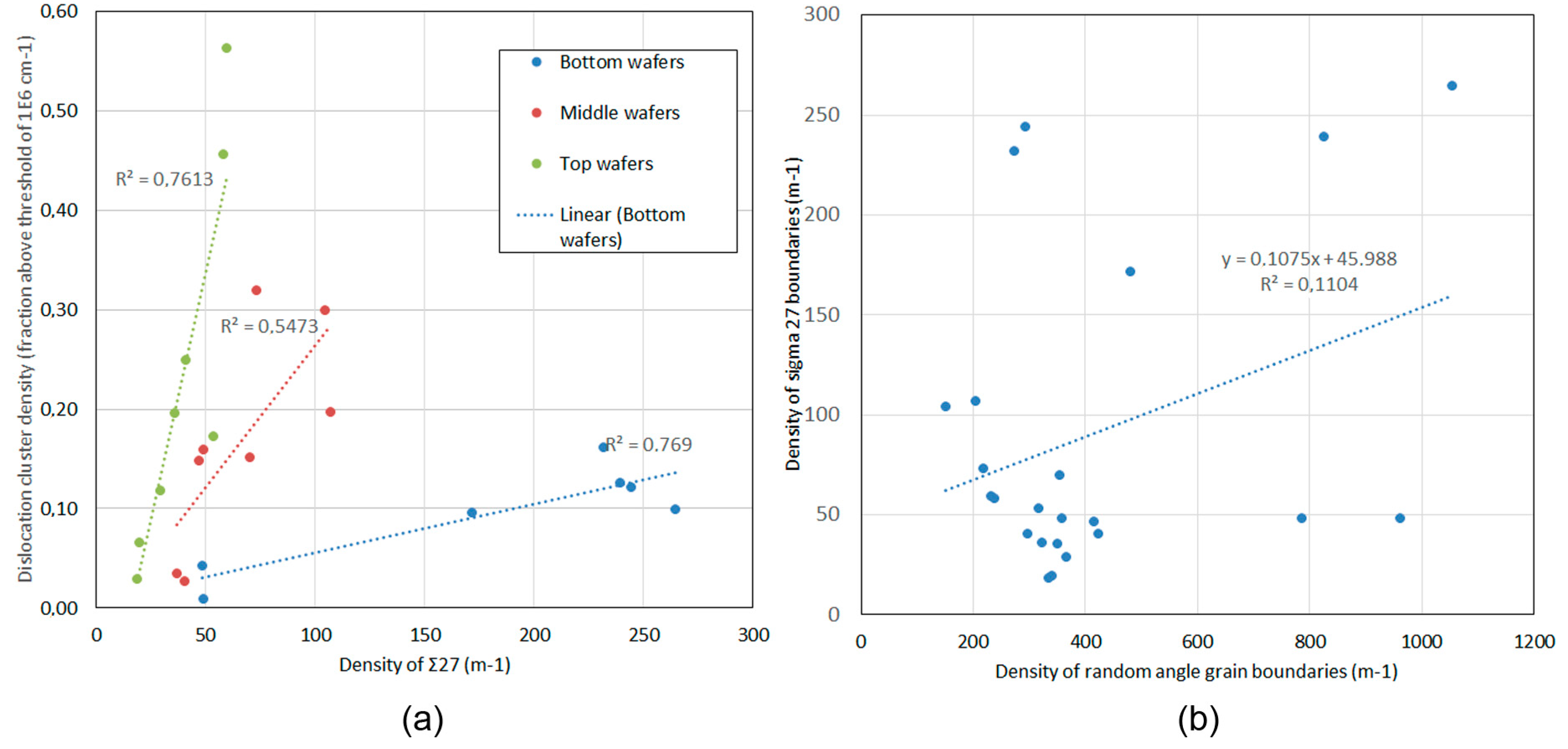
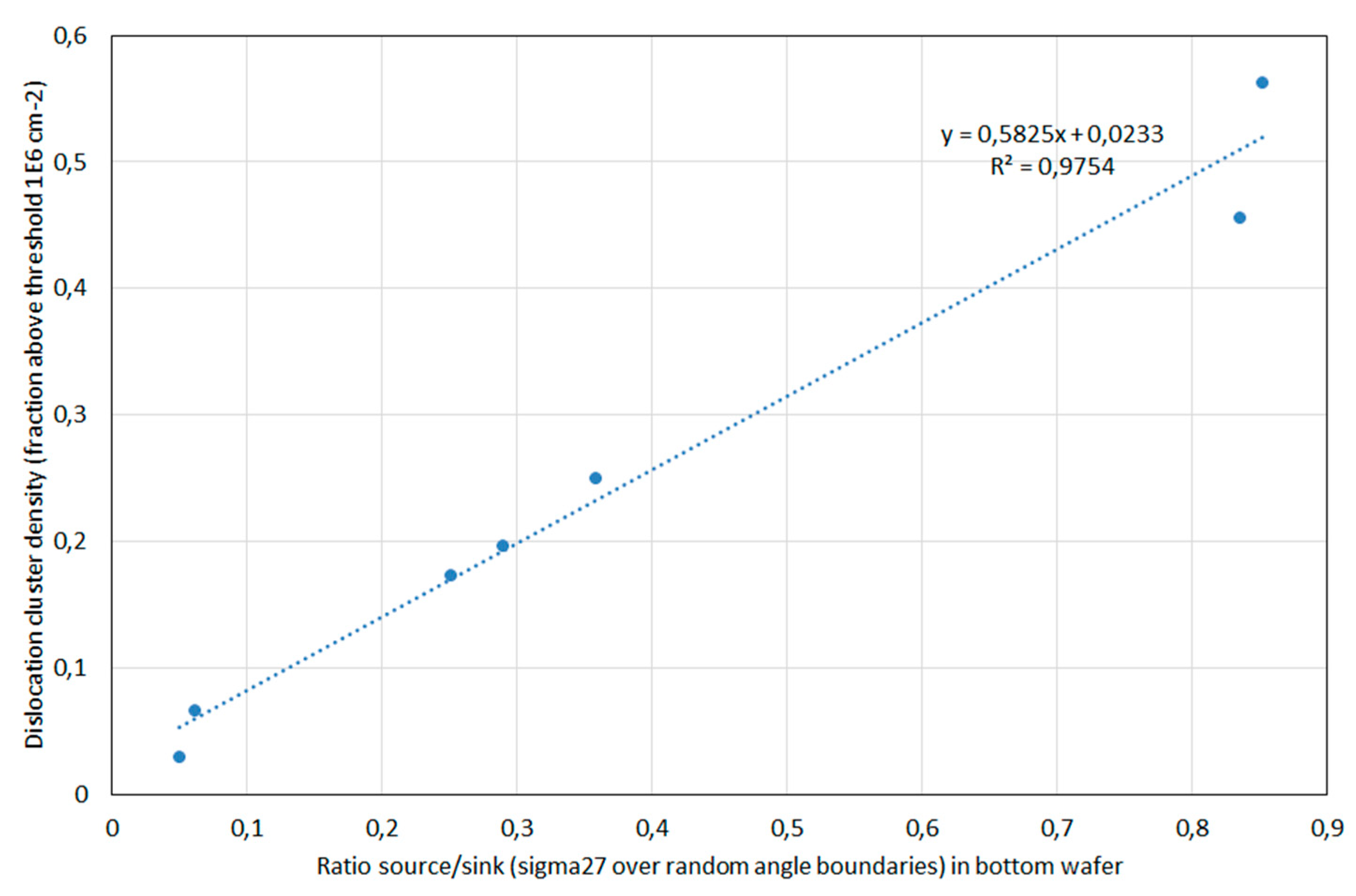
3.3. Dislocation Density
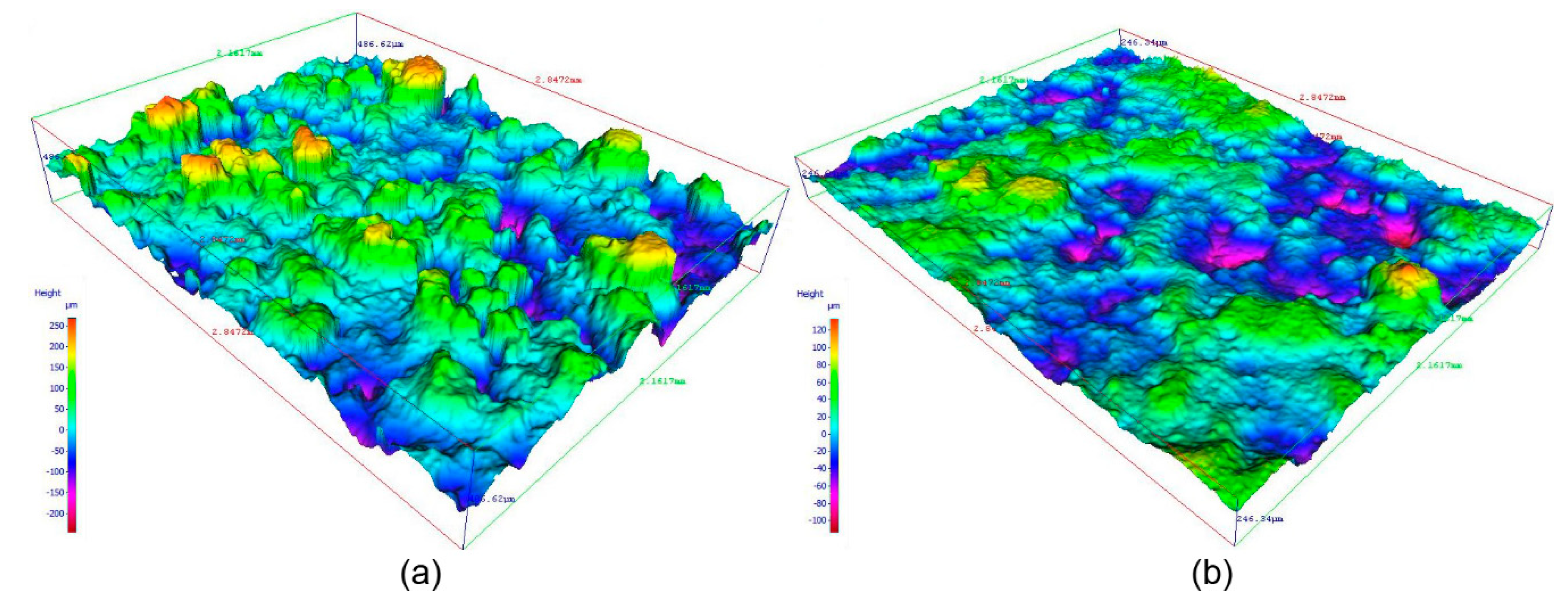
3.4. Coating Morphology
4. Discussion
4.1. Mechanisms Controlling Grain Boundary Density
4.2. Relationship between Grain Boundaries and Dislocations
5. Conclusions
Author Contributions
Funding
Acknowledgments
Conflicts of Interest
References
- Fraunhofer ISE: Photovoltaics Report. Available online: https://www.ise.fraunhofer.de/content/dam/ise/de/documents/publications/studies/Photovoltaics-Report.pdf (accessed on 10 August 2018).
- Yang, Y.M.; Yu, A.; Hsu, B.; Hsu, W.C.; Yang, A.; Lan, C.W. Development of high-performance multicrystalline silicon for photovoltaic industry. Prog. Photovolt. Res. Appl. 2013, 23, 340–351. [Google Scholar] [CrossRef]
- Lan, C.W.; Lan, A.; Yang, C.F.; Hsu, H.P.; Yang, M.; Yu, A.; Hsu, B.; Hsu, W.C.; Yang, A. The emergence of high-performance multi-crystalline silicon in photovoltaics. J. Cryst. Growth 2017, 468, 17–23. [Google Scholar] [CrossRef]
- Ryningen, B.; Stokkan, G.; Kivambe, M.; Ervik, T.; Lohne, O. Growth of dislocation clusters during directional solidification of multicrystalline silicon ingots. Acta Mater. 2011, 59, 7703–7710. [Google Scholar] [CrossRef]
- Stokkan, G. Relationship between dislocation density and nucleation in multicrystalline silicon. In Proceedings of the 6th International Symposium on Advanced Science and Technology of Silicon Materials, Kona, HI, USA, 19–23 November 2012; pp. 227–230. [Google Scholar]
- Kohler, D.; Zuschlag, A.; Hahn, G. On the origin and formation of large defect clusters in multicrystalline silicon solar cells. Sol. Energy Mater. Sol. Cells 2014, 120, 275–281. [Google Scholar] [CrossRef]
- Ervik, T.; Kivambe, M.; Stokkan, G.; Ryningen, B.; Lohne, O. Dislocation formation at ∑ = 27a boundaries in multicrystalline silicon for solar cells. In Proceedings of the 26th European Photovoltaic Solar Energy Conference and Exhibition, Hamburg, Germany, 5–9 September 2011; pp. 1895–1899. [Google Scholar]
- Kohyama, M.; Yamamoto, R.; Doyama, M. Structures and energies of symmetrical 011 tilt grain boundaries in silicon. Phys. Status Solidi B 1986, 137, 11–20. [Google Scholar] [CrossRef]
- Garg, A.; Clark, W.A.; Hirth, J.P. Dissociated and faceted large-angle coincident-site-lattice boundaries in silicon. Philos. Mag. A 1989, 59, 479–499. [Google Scholar] [CrossRef]
- Garg, A.; Clark, W.A.; Hirth, J.P. Dislocation generation at near-coincidence site lattice grain boundaries during silicon directional solidification. J. Cryst. Growth 2015, 411, 12–18. [Google Scholar]
- Stokkan, G.; Hu, Y.; Mjøs, Ø.; Juel, M. Study of evolution of dislocation clusters in high performance multicrystalline silicon. Sol. Energy. Mater. Sol. Cells 2014, 130, 679–685. [Google Scholar] [CrossRef]
- Möller, H.J.; Funke, C.; Kreßner-Kiel, D.; Würzner, S. Growth optimization of multicrystalline silicon. Engrgy Procedia 2011, 3, 2–12. [Google Scholar] [CrossRef]
- Ekstrøm, K.E.; Undheim, E.; Stokkan, G.; Arnberg, L.; Di Sabatino, M. Beta-Si3N4 particles as nucleation sites in multicrystalline silicon. Acta Mater. 2016, 109, 267–274. [Google Scholar] [CrossRef]
- Sopori, B.L. A new defect etch for polycrystalline silicon. J. Electrochem. Soc. 1984, 131, 667–672. [Google Scholar] [CrossRef]
- Sopori, B.; Wei, C.; Yi, Z.; Madjdpour, J. High-speed mapping of grown-in defects and their influence in large-area silicon photovoltaics. J. Cryst. Growth 2000, 210, 346–350. [Google Scholar] [CrossRef]
- Stokkan, G. Characterisation of dislocation density of multicrystalline silicon wafers using the PVScan 6000. In Proceedings of the 22nd European Photovoltaic Solar Energy Conference, Milan, Italy, 3–7 September 2007; pp. 1282–1286. [Google Scholar]
- Stokkan, G. Twinning in multicrystalline silicon for solar cells. J. Cryst. Growth 2013, 384, 107–113. [Google Scholar] [CrossRef]
- Stokkan, G.; Stoss, A.; Kivambe, M.; Ervik, T.; Ryningen, B.; Lohne, O. Distribution of Grain Boundary Types in Multicrystalline Silicon. In Proceedings of the 28th European Photovoltaic Solar Energy Conference and Exhibition, Paris, France, 30 September–4 October 2013; pp. 1418–1421. [Google Scholar]
- Ryningen, B.; Bellmann, M.; Kvande, R.; Lohne, O. The effect of crucible coating and the temperature field on minority carrier lifetime in directionally solidified multicrystalline silicon ingots. In Proceedings of the 27th European Photovoltaic Solar Energy Conference and Exhibition, Frankfurt, Germany, 24–28 September 2012. [Google Scholar]
- Tsoutsouva, M.G.; Duffar, T.; Chaussende, D.; Kamguem, M. Undercooling measurement and nucleation study of silicon droplets on various substrates. J. Cryst. Growth 2016, 451, 103–112. [Google Scholar] [CrossRef]
- Brynjulfsen, I.; Arnberg, L. Nucleation of silicon on Si3N4 coated SiO2. J. Cryst. Growth 2011, 331, 64–67. [Google Scholar] [CrossRef]
- Undheim, E.; Ekstrøm, K.E.; Arnberg, L.; Holmestad, R.; Di Sabatino, M. The effect of holding time on the size distribution of -Si3N4 particles and nucleation undercooling in multicrystalline silicon. Phys. Status Solidi (C) Curr. Top. Phys. 2016, 13, 822–826. [Google Scholar] [CrossRef]
- Fujiwara, K.; Maeda, K.; Usami, N.; Sazaki, G.; Nose, Y.; Nomura, A.; Shishido, T.; Nakajima, K. In situ observation of Si faceted dendrite growth from low-degree-of-undercooling melts. Acta Mater. 2008, 56, 2663–2668. [Google Scholar] [CrossRef]
- Undheim, E.; Maeda, K.; Arnberg, L.; Holmestad, R.; Fujiwara, K.; Di Sabatino, M. In-situ studies of multicrystalline silicon nucleation and growth on α-and β-Si3N4 coated substrates. J. Cryst. Growth 2018, 482, 75–84. [Google Scholar] [CrossRef]
- Oriwol, D.; Trempa, M.; Sylla, L.; Leipner, H.S. Investigation of dislocation cluster evolution during directional solidification of multicrystalline silicon. J. Cryst. Growth 2017, 463, 1–9. [Google Scholar] [CrossRef]
- Oriwol, D.; Carl, E.R.; Danilewsky, A.N.; Sylla, L.; Seifert, W.; Kittler, M.; Leipner, H.S. Small-angle subgrain boundaries emanating from dislocation pile-ups in multicrystalline silicon studied with synchrotron white-beam X-ray topography. Acta Mater. 2013, 61, 6903–6910. [Google Scholar] [CrossRef]
- Lehmann, T.; Reimann, C.; Meissner, E.; Friedrich, J. Clarification of the relation between the grain structure of industrial grown mc-Si and the area fraction of electrical active defects by means of statistical grain structure evaluation. Acta Mater. 2016, 106, 98–105. [Google Scholar] [CrossRef]
- Trempa, M.; Kupka, I.; Kranert, C.; Lehmann, T.; Reimann, C.; Friedrich, J. Evolution of grain structure and recombination active dislocations in extraordinary tall conventional and high performance multi-crystalline silicon ingots. J. Cryst. Growth 2017, 459, 67–75. [Google Scholar] [CrossRef]


| Ingot Label | Initial Growth | Size | Coating |
|---|---|---|---|
| VH1 | non-seeded | G5 | regular |
| VH2 | non-seeded | G5 | regular |
| G4VHP | non-seeded | G4 | enhanced roughness |
| MS/multiseed | seeded | G5 | not relevant |
| Similar to G4VHP | Similar to VH1/VH2 | |||
|---|---|---|---|---|
| 5× | corner | center | corner | center |
| Ra (µm) | 13.96 | 8.35 | 15.46 | 5.15 |
| Sm (µm) | 408.58 | 403.46 | 288.62 | 241.56 |
| 20× | corner | center | corner | center |
| Ra(µm) | 5.36 | 1.64 | 5.42 | 2.27 |
| Data Series | Twins | Σ27 | RAGB | Source/Sink | ||||
|---|---|---|---|---|---|---|---|---|
| Slope | R2 | Slope | R2 | Slope | R2 | Slope | R2 | |
| bottom wafer | 0.16 | 0.12 | 0.23 | 0.77 | −0.17 | 0.32 | 0.19 | 0.67 |
| middle | −0.73 | 0.08 | 1.33 | 0.54 | −1,5 | 0.60 | 0.53 | 0.55 |
| top | 1.43 | 0.30 | 4.67 | 0.76 | −6.35 | 0.84 | 3.38 | 0.90 |
| dislocations in top vs. grain boundaries in bottom | 0.03 | 0.00 | 0.66 | 0.44 | −1.0 | 0.76 | 0.88 | 0.98 |
| σ27 vs. ragb | 0.43 | 0.11 | ||||||
© 2018 by the authors. Licensee MDPI, Basel, Switzerland. This article is an open access article distributed under the terms and conditions of the Creative Commons Attribution (CC BY) license (http://creativecommons.org/licenses/by/4.0/).
Share and Cite
Stokkan, G.; Song, A.; Ryningen, B. Investigation of the Grain Boundary Character and Dislocation Density of Different Types of High Performance Multicrystalline Silicon. Crystals 2018, 8, 341. https://doi.org/10.3390/cryst8090341
Stokkan G, Song A, Ryningen B. Investigation of the Grain Boundary Character and Dislocation Density of Different Types of High Performance Multicrystalline Silicon. Crystals. 2018; 8(9):341. https://doi.org/10.3390/cryst8090341
Chicago/Turabian StyleStokkan, Gaute, Adolphus Song, and Birgit Ryningen. 2018. "Investigation of the Grain Boundary Character and Dislocation Density of Different Types of High Performance Multicrystalline Silicon" Crystals 8, no. 9: 341. https://doi.org/10.3390/cryst8090341
APA StyleStokkan, G., Song, A., & Ryningen, B. (2018). Investigation of the Grain Boundary Character and Dislocation Density of Different Types of High Performance Multicrystalline Silicon. Crystals, 8(9), 341. https://doi.org/10.3390/cryst8090341