1. Introduction
High-quality multicrystalline (mc) Si ingot is beneficial for fabricating high efficiency solar cells. Grain boundaries (GBs), dislocations, and their interactions with impurities are the major factors limiting the material quality [
1,
2,
3]. Generally, GBs and dislocations in mc-Si act as carrier recombination centers due to the defect levels introduced by impurities [
4,
5,
6]. Our previous study has clarified that electrical activities of large-angle GBs were affected by both the boundary character and Fe impurity concentration [
7] particularly, dislocation clusters and small-angle GBs which remain the most detrimental defects for solar cells [
8,
9]. To decrease the effect of GBs and dislocations, many efforts have been made to control the growth and defect density, such as dendrite Si [
10], mono-like Si [
11,
12], and high-performance (HP) mc-Si [
13,
14]. Mono-like Si is quasi monocrystalline based on single crystal seed, whilst HP mc-Si is small-grains grown on fine grain seeds. Despite the different grain structure, the mono-like Si showed a similar carrier lifetime to that of the HP mc-Si [
15]. This was probably because of impurity contamination during the melting of raw materials in the initial stage of seed growth. In seeded growth, the difficulty is the optimization of the growth procedure. During the melting of raw materials, seeds should be kept solid and directional growth on seeds is expected. If the seed is melted, impurities may diffuse into Si melt. In the case of joint seeds, the generation of dislocations from seed joints is difficult to avoid.
On the other hand, seed-free dendrite growth from highly undercooled melts, is a unique method for growing mc-Si with large grain size. Dendrite growth is promoted in the initial stage along the bottom wall of the crucible. The dendrite crystals formed at the bottom act as seed crystals for a following directional growth process. Mc-Si based on dendrite growth, tended to have preferential growth direction, large grain, and exhibited good photovoltaic performance close to single crystalline Si [
10]. The growth mechanism of dendrite Si is related with parallel-twin formation during the faceted growth [
16]. Inside dendrite grain, most GBs are twins, which are less electrically active compared with irregular GBs. However, the in-plane growth of dendrite crystals is difficult to control. At the borders of dendrite grains, the formation of random GBs and dislocations may take place. Because of the different growth mechanism, the behavior of defects and their interaction with impurities may differ from conventional mc-Si. Until now, there is a lack of study on the defects in this novel mc-Si material. Recently, we carried out electron-beam-induced current (EBIC) observations on Si dendrites and the results will be reported here.
When we performed EBIC observation on dendrite Si, abnormally bright EBIC contrast was sometimes found at GBs and intragranular defects. Bright EBIC contrast at GBs is not common and is probably of specific origins. Only a few papers have discussed about the bright EBIC contrast at GBs; for instance, Seibt et al. [
17] have observed bright EBIC contrast of NiSi
2 platelets in n-type Si. The bright contrast was caused by partially charge collection at the precipitate. Kittler et al. [
18] have revealed enhanced charge carrier transport along GBs in directly bonded Si bi-crystals. The phenomenon was explained using a shallow band model, in which a collecting electron channel was formed at the shallow band introduced by boundary dislocation networks. Breitenstein et al. [
19,
20] have done a comprehensive study about current shunts at GBs in mc-Si solar cells. They performed EBIC imaging from both the frontside and backside of a
p-n junction and discovered GB contrast reversing from dark to bright. The origin of this phenomenon was attributed to the presence of conducting SiC filaments crossing throughout the cell. In this study, we will compare the grains with and without dendrite growth, concerning the GBs and impurity incorporation. The origin of bright EBIC contrast at certain defects will be explored.
2. Experimental
The sample used was the mc-Si ingot by dendrite growth method developed by Fujiwara and his co-workers at Tohoku University. The Si source (
p-type, 1–5 Ω cm) was melted in a quartz crucible, in an argon gas atmosphere. Dendrite growth was achieved by controlling the undercooling ΔT > 10 K. The growth velocity of the dendrite in this study was around 160 μm/s. The details of growth have been described in previous studies [
21]. The ingot size was about 10 × 20 mm
2 and 8 mm height.
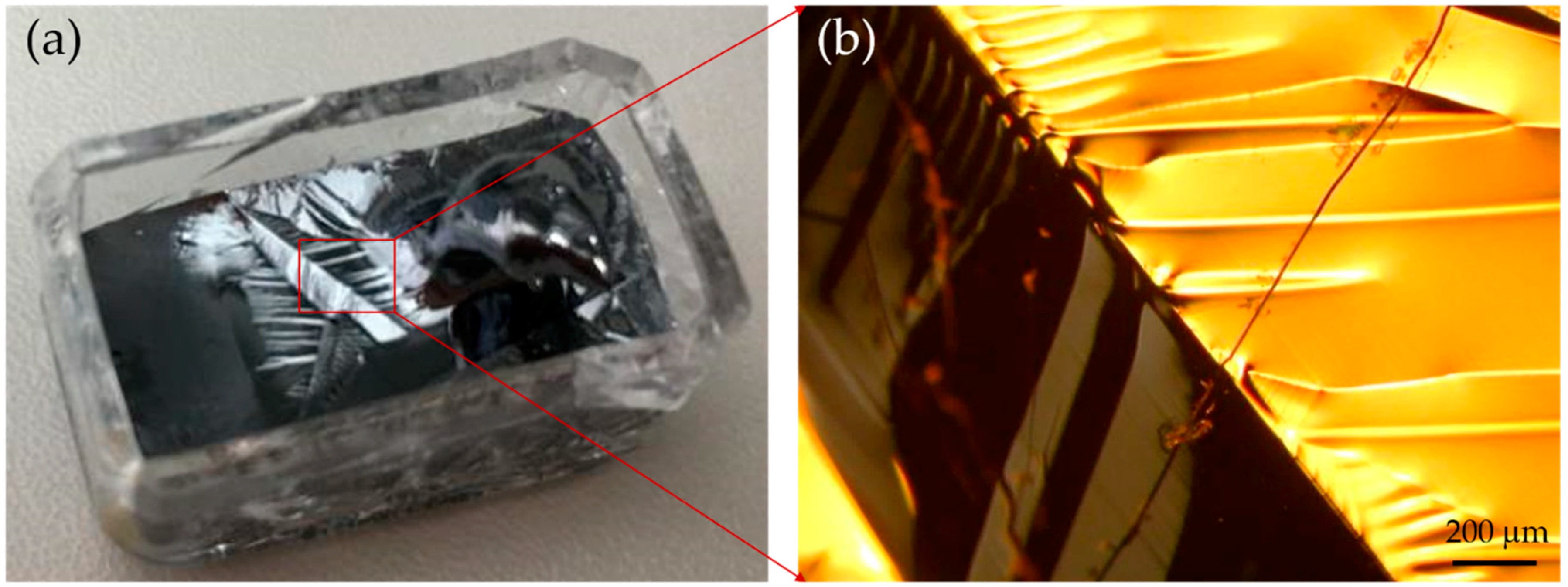
Figure 1a shows a photograph of the mc-Si ingot containing dendritic structures.
Figure 1b shows an optical image of the dendrite area. The growth mechanism of faceted dendrites has been reported in References [
16,
21]. The surface of the dendrite is bounded by {111} planes, and at least two parallel twins exist at the center of the dendrite.
For EBIC study, mirror surfaces were obtained using chemo-mechanical polishing. It should be noted that during slicing and polishing, cracks were easily introduced due to large residual strain in the ingots. Schottky contacts were prepared by e-beam deposition of Al with a thickness of 30 nm. Al wire-bonding was used for the electrical connection. EBIC measurement was conducted with a JSM-7600F (JEOL Ltd., Tokyo, Japan) field emission scanning electron microscope (FE-SEM) at room temperature. If not mentioned, the accelerating voltage was 20 kV for EBIC observation. Electron back-scattered diffraction (EBSD) analysis of GB character was done with a JSM-7001F FE-SEM (JEOL Ltd., Tokyo, Japan), with EBSD detector at 15 kV. To investigate GB structure and impurity precipitates, thin foil specimens were prepared using a focused ion beam (FIB). Transmission electron microscopy (TEM) and energy dispersive X-ray spectroscopy (EDS) analysis, were performed using a EM-002BF (TOPCON TECHNOHOUSE, Tokyo, Japan) microscope at 200 kV.
3. Results and Discussion
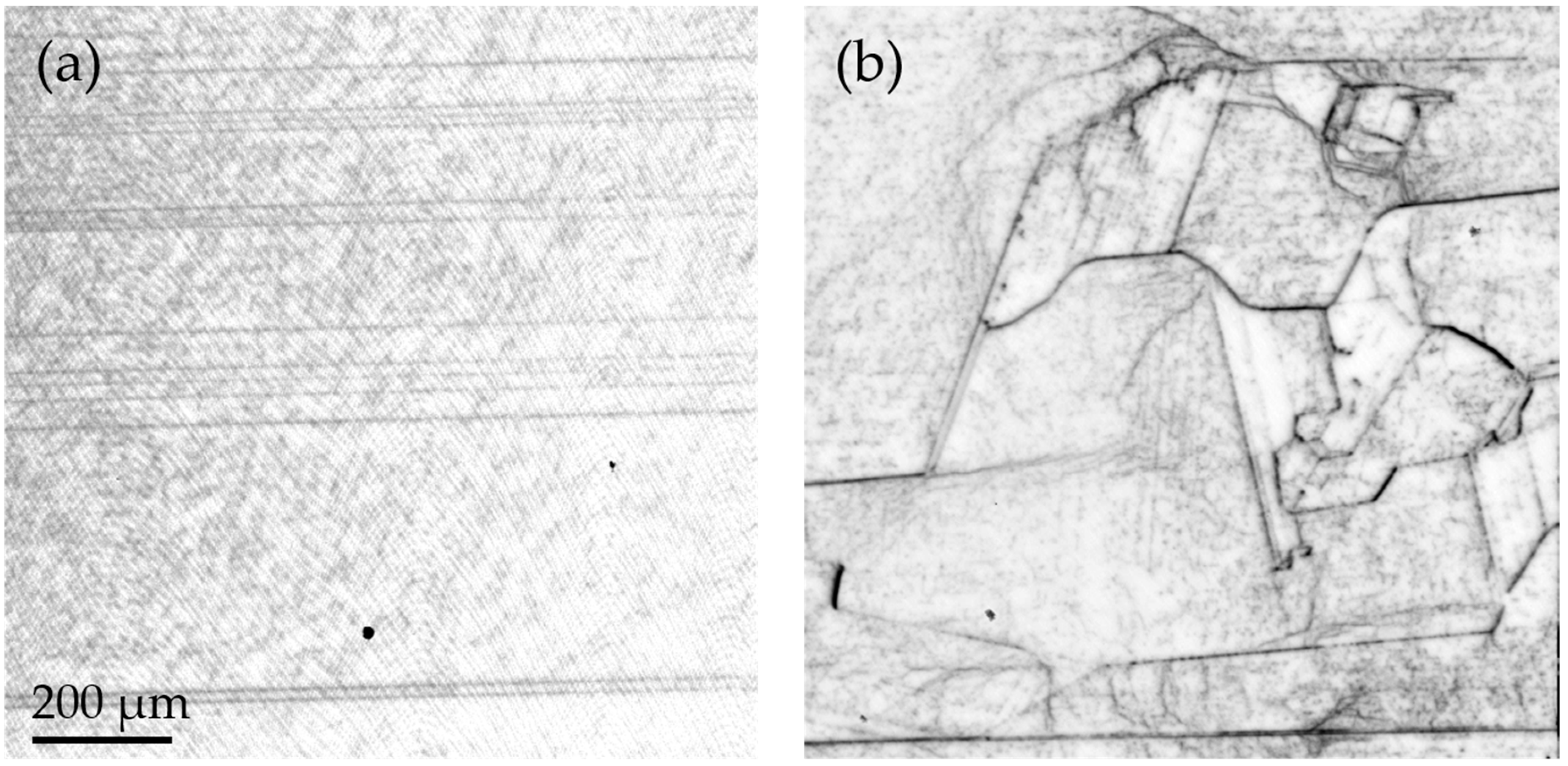
Figure 2 shows two EBIC images taken over dendrite and non-dendrite grains. The dendrite region had large-size grain and straight parallel twins inside, as shown in
Figure 2a. Outside of the dendrite (
Figure 2b), there existed smaller grains and irregular GBs with either strong or weak contrast depending on boundary character, as usually observed in normal mc-Si. In both cases, GBs and intragranular defects appeared with dark contrast in EBIC, indicating the presence of recombination centers due to impurity contamination introduced during crystal growth. The parallel twins were probably formed during faceted growth. It is noted that dislocations existed around these twins. Their density seemed to decrease gradually along twin growth direction. One explanation is that initial dendrite growth under high undercooling will be accompanied with large strain, and dislocation generation during cooling will occur. On the other hand, in the region without dendrites, a high density of intragrain dislocations and small-angle boundaries will exist due to dislocation multiplication. It should be noted that crucible size was very small in this study, and the growth conditions were largely different from those for large ingot growth. Therefore, the quality of the dendrite in this study became much worse compared to that of the dendrite in large ingots.
During EBIC observations of dendrites, we sometimes found GBs and dislocations with bright EBIC contrast.
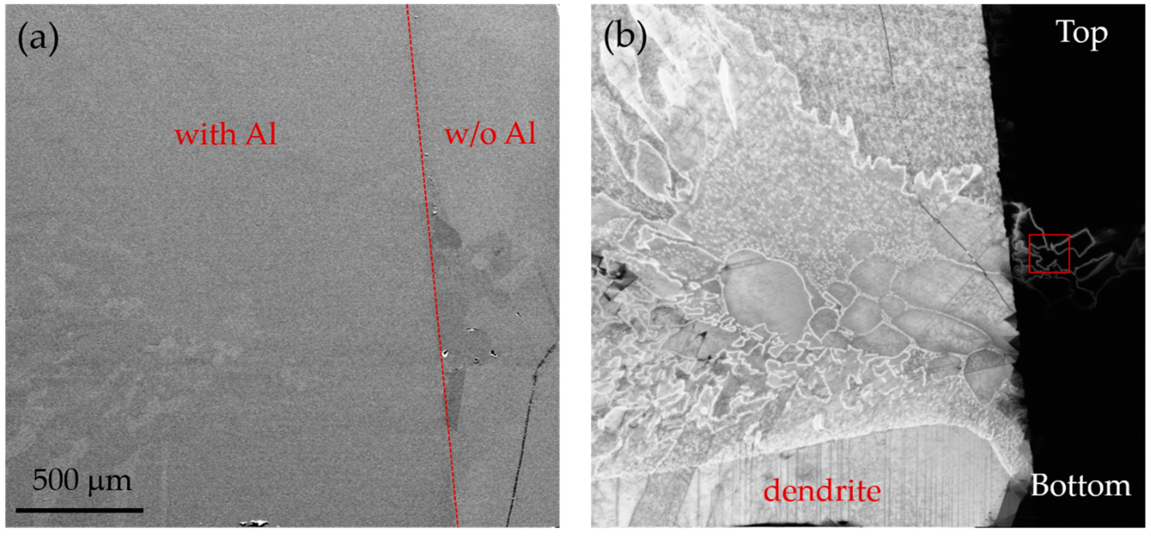
Figure 3 shows the end of the Schottky area. The bright region in the EBIC image is covered by Al Schottky contact. This area is the vertical cross-section from bottom to top. There were several features: (1) A large part of the grains, except the bottom dendrite, were decorated with bright contrast at GBs and intragranular defects; (2) Parallel twins and dislocations in the bottom dendrite grain appeared with dark contrast; and (3) In the region outside of Al contact, bright contrast was also visible at some GBs within a distance of about 400 μm, close to the Al Schottky.
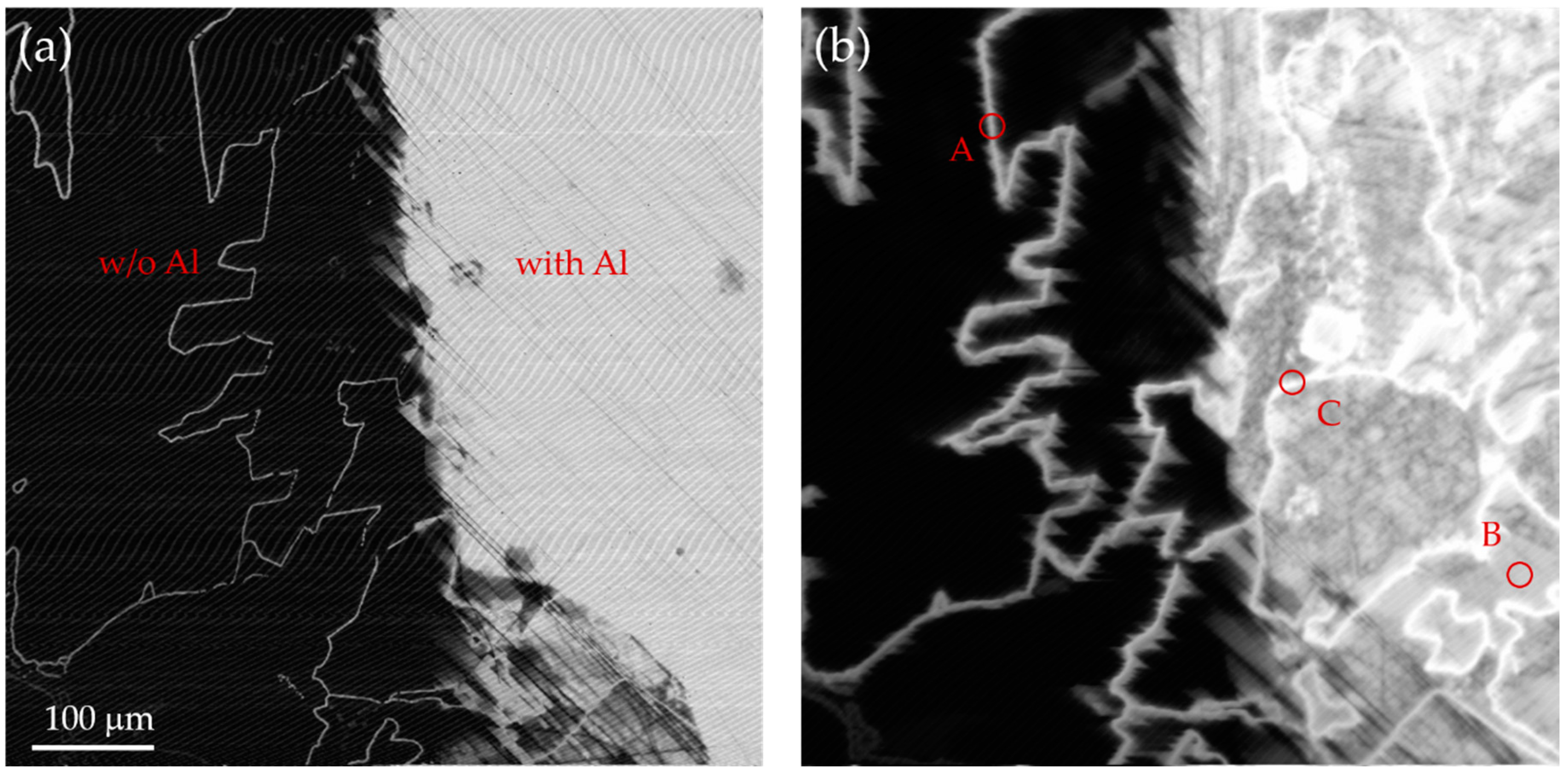
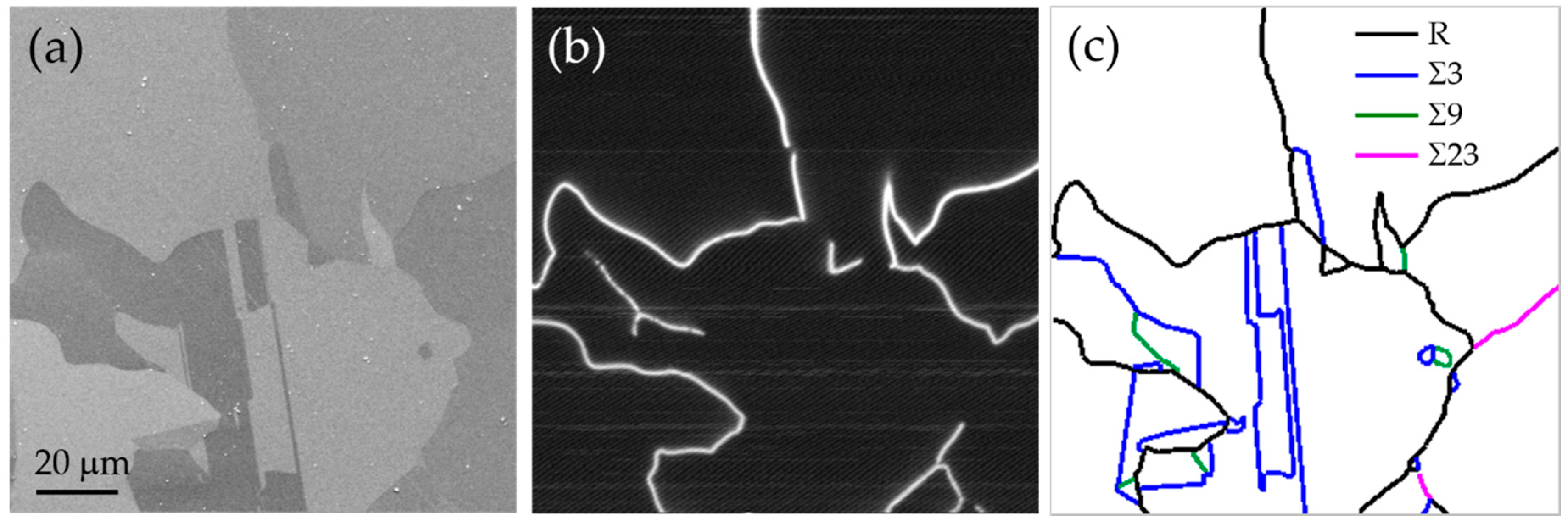
Figure 4 shows the magnified secondary electron (SE), EBIC, and EBSD images of the square region denoted in
Figure 3b. The SE and EBIC images were taken at 7 kV. Grains were visible in the SE image due to electron channeling contrast. The GB character was indicated in the EBSD image. By correlating EBIC with EBSD, it was found that the bright GBs were mainly random and high-Σ type.
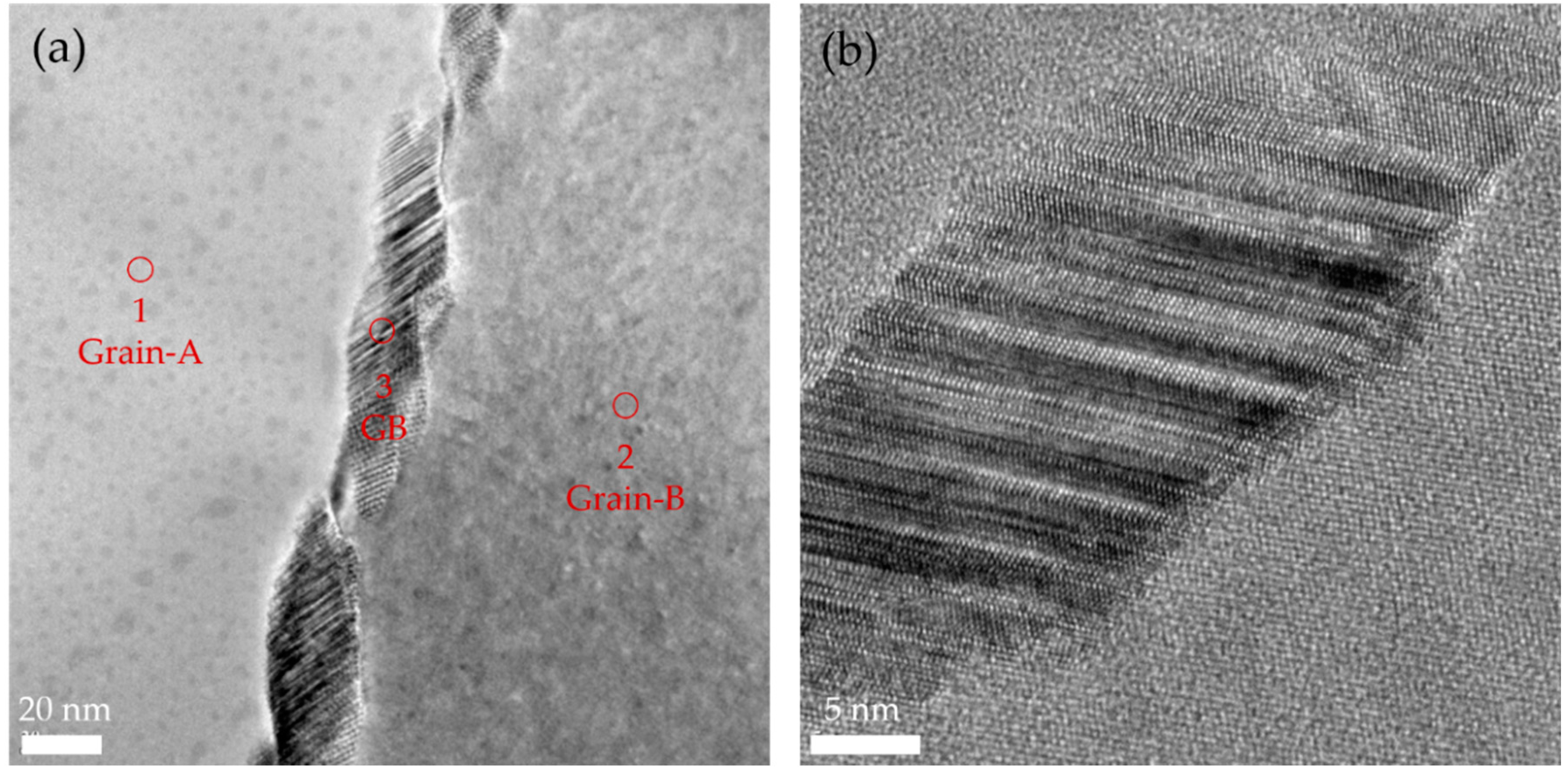
Figure 5 shows bright field TEM images, of a bright EBIC GB with random character. The boundary was not smooth, and precipitates existed on it. EDS element mapping (not shown here), suggested the enrichment of carbon at bright GB. Three positions, denoted in
Figure 5a, were chosen for EDS analysis and the result is listed in
Table 1. The inclusions at the boundary turned out to be SiC.
Figure 5b shows a high resolution TEM image of SiC precipitate. The precipitates were mainly cubic SiC with complex stacking sequences and twins. Based on the EBIC and TEM observations, bright EBIC contrast suggested that such GBs were conductive. These GBs were covered with SiC precipitates. Breitenstein et al. [
19] found that SiC shunts showed n-type conduction due to nitrogen incorporation from silicon nitride coating. In this study, the crucible was not coated silicon nitride, and the Si melt directly contacted with quartz crucible. It is speculated that the incorporation of oxygen may be one of the origins of conductivity; however, due to the detection limit of EDS, the presence of oxygen could not be confirmed. The presence of SiC precipitates may result in the leakage and breakdown of solar cells and should be avoided.
Figure 6 compares the EBIC images taken at 20 kV and 5 kV, of another border region of Al Schottky. The penetration depth of the e-beam was about 3 μm and 300 nm respectively, based on Monte Carlo simulation of electron trajectory. In the Al Schottky region, there was no obvious contrast of GBs and intragranular defects at 5 kV, only dark lines due to surface scratches were visible; at 20 kV, GBs were visualized with bright contrast. On the other hand, the GBs outside of Al Schottky were bright at both accelerating voltages. At higher accelerating voltage, they became broader, suggesting that the bright contrast seemed to penetrate deep into the bulk along GB. The geometry effect, such as the inclination of boundary plane may have affected their appearance.
Table 2 lists the beam parameters and EBIC currents detected from several regions. The probe current was 0.15 nA at 5 kV, and 0.58 nA at 20 kV. The background EBIC current collected by Al Schottky was about 270 nA at 5 kV, and 860 nA at 20 kV. In the case of 5 kV, most of the generated carriers were inside the depletion layer of Al Schottky (depletion region width ~280 nm) and could be efficiently collected without significant effect from GBs. At 20 kV, carriers were generated in a deeper region and underwent diffusion and recombination before being collected by Al Schottky. If GB channels exist, an increased current signal (1020 nA) could be detected. The bright contrast at GBs in the regions outside of Al, reflected the pure effect of GB channels. It should be noted that only GBs close to Al Schottky, within 400 μm as shown in
Figure 3, could be observed with bright contrast, whilst GBs that stayed far away and intragranular defects, have no contrast. This may have indicated that a GB channel becomes active only when it is connected to the electrode. Similar phenomena has been reported in the EBIC study, NiSi
2 platelets [
17]. When the precipitate was electrically coupled with Schottky metal, bright EBIC contrast could be observed.
Finally, we discuss the difference between dendrite and non-dendrite grains. It is rare to see bright defect contrast inside the dendrite grains, which means that the SiC hardly precipitates in these grains. One reason is that most GBs in dendrites are coherent twin boundaries with few dislocations. Hence, the precipitation of SiC does not happen easily. There may exist another reason. When we compared the dislocations in the dendrite and non-dendrite grains, the former always appeared with dark contrast whereas the latter, sometimes with bright contrast. This suggested that there was a difference in carbon concentration. Since the segregation coefficient of carbon in silicon is small (k ~ 0.07), the concentration of carbon increases in melt during solidification. As a result, high concentration of carbon will be found in the grains solidified last. In the case of dendrite growth, dendrite grain can grow faster than the others as confirmed by in-situ observation [
10]. It will leave a higher carbon concentration in non-dendrite grains solidified last. Thus, it explains why SiC precipitate occurs preferentially in non-dendrite grains, but not in dendrite regions.
Si dendrite growth can realize large grain and reduce the number of irregular GBs. It is expected to be utilized for the growth of high quality mc-Si. However, during dendrite growth, because of the significant difference in growth speed between dendrite and non-dendrite regions, severe segregation of carbon may take place in non-dendrite grains solidified last. Since SiC may act as a current shunt, it is necessary to suppress their formation during the initial growth stage.

 ,
, 


