Abstract
Nanoindentation morphologies of crystalline copper have been probed at the grain scale. Experimental tests have been conducted on nanocrystalline (NC), ultrafine-grained (UFG), and coarse-grained (CG) copper samples with a new Berkvoich indenter at the strain rate of 0.04/s without holding time at an indentation depth of 2000 nm at room temperature. As the grain size increases, the height of the pile-up around the residual indentation increases and then exhibits a slightly decrease in the CG Cu. The maximum of the pile-up in the CG Cu obviously deviates from the center of the indenter sides. Our analysis has revealed that the dislocation motion and GB activities in the NC Cu, some cross- and multiple-slip dislocations inside the larger grain in the UFG Cu, and forest dislocations from the intragranular Frank-Read sources in the CG Cu would directly induce this distinct pile-up effect.
1. Introduction
The nanoindentation technique has been widely used to characterize the mechanical properties of bulk- and thin-film materials on nano- and microscopic scales, such as elastic modulus (E) and hardness (H). In order to minimize the impact of blunting from the indenter, the involved mechanical parameters in this contact area calibration are acquired from the indentation of a standard fused silica sample. However, in some cases there exists an apparent upward extrusion at the edge of the contact with the indenter in some metals, known as pile-up, which means that the actual contact area is larger than the value calculated by the Oliver-Pharr method [1]. Some studies have reported that the true contact area is 60% larger than the measured value as serious pile-up occurs, leading to the overestimation of the E and H [2,3,4,5,6,7]. Therefore, an understanding of the formation of the indentation pile-up in various materials and loading conditions under nanoindentation testing is invaluable.
To date, there is no convince evidence to suggest that any new modified method considering pile-up at a larger indentation depth could bring more accurate measurement results, and the Oliver-Pharr method still is considered to provide relatively reliable E and H values. Even so, the morphology of residual impression could also present other useful information or parameters in deformed materials. For example, many studies have shown that the formation of pile-up is closely related to the ratio of the yield stress () to E, the ratio of the final indentation depth hf to the maximum indentation depth hmax, and the strain hardening exponent (n). Metallic materials with smaller values of and n usually exhibit larger pile-up height, but an accurate determination of these two parameters in the indentation process becomes impossible. Therefore, the easily measured hf/hmax from the load-displacement curve can be used to determine the prevalence of the pile-up. It has been suggested that for materials with low work hardening ability, the amount of pile-up would become obvious as the ratio of hf/hmax becomes larger than 0.7 [2,3]. Interestingly, most of the theoretical development reports were based on numerical modeling [5,8,9,10,11,12], with very limited experimental data being used to explain this phenomenon. As for crystalline materials, it has been widely accepted that the grain boundary (GB) mediated deformation process can operate effectively in materials with a grain size smaller than 500 nm. The concurrently occurred dislocation activity grouping with GB activities could promote the formation of micro (narrow) shear bands under tensile or compression testing. Although some reports have studied the effect of work-hardening grain orientation on pile-up formation in coarse-grained (CG) metals [3,13], other factors such as grain size and deformation mechanisms have rarely been mentioned.
The aim of the present work is to establish the relationship between the pile-up effect and grain size in crystalline materials. Nanocrystalline (NC), ultrafine-grained (UFG), and CG copper samples were detected by nanoindentation at room temperature at an indentation depth of 2000 nm, and their pile-up effect around the residual impressions were systemically studied. Deformation mechanism transformation was used to explain why the pile-up effect exhibits different morphologies in crystalline materials with different grain sizes.
2. Experiments Details
The bulk NC/UFG Cu specimens with different grain sizes used in this article were synthesized by electric brush-plating on a substrate of copper sheets with a bath only containing CuSO4·5H2O (180–220 g/L); the detailed processes are presented in References [14,15,16]. A commercial coarse-grained (CG) copper sheet with thickness of 2 mm and purity of 99.99 wt % was annealed at a temperature of 800 °C for 24 h, and prepared for a contrastive experiment. Foil samples for transmission electron microscope (TEM, JEM-2100F, JEOL, Tokyo, Japan) observation under an accelerating voltage of 200 kV were prepared by cutting, polishing, and dimpling by argon-ion milling (EMRES101) at 5 kV. Square-shaped nanoindentation specimens of NC/UFG/CG Cu with a gauge size of 30 × 30 × 2 mm3 were cut, and then mechanically grinded with SiC papers, and finally polished with a microcloth using a slurry of 0.5 µm alumina. To acquire reliable nanoindentation data, the surfaces of the test specimens were mechanically polished to mirror finishing, and then their mechanical properties were characterized at room temperature by a nanoindenter (Agilent-G200, Keysight, Santa Rosa, CA, USA) with a Berkovich diamond indenter. All of the samples were loaded at strain rates of 0.4/s, 0.04/s, and 0.004/s to the indentation depth of 2000 nm without holding time under the procedure of the continuous stiffness measurement (CSM). The thermal drift rate prior to testing was limited below 0.025 nm/s and the indentation under same condition was repeated at least 10 times. The surface morphology of the residual impression obtained at a strain rate of 0.04/s was observed by laser confocal microscopy (LSM, OLS4500, OLYMPUS, Tokyo, Japan).
3. Results
3.1. TEM Observation
Figure 1 gives the TEM bright images of the typical microstructures of the as-brush-plated NC/UFG Cu. It reveals that these materials consist of uniformly equiaxed grains with random crystalline orientations and predominant high-angle grain boundaries (GBs). Grain size was measured from the statistical analysis of 500 grains taken from several TEM images, and the average values of these materials are 30 nm, 150 nm, and 300 nm, respectively.
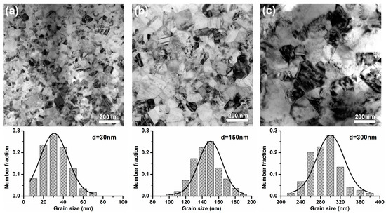
Figure 1.
TEM bright-field images of the as-brush-plated NC/UFG Cu: (a) 30 nm Cu; (b) 150 nm Cu; (c) 300 nm Cu.
3.2. Residual Morphology of the Impression
Figure 2 shows the load-displacement (P-h) curves obtained at a strain rate of 0.04/s to the indentation depth of 2000 nm without holding time on these four materials. It can be seen that as the grain size decreases, the acquired load at a given displacement in the loading stage increases rapidly and the slope value of the P-h curves during the unloading regime decreases obviously. To assess the effect of the pile-up in the indenters, Table 1 summarizes the ratio of hf/hmax in these four materials. Clearly, this ratio decreases steadily as the grain size decreases.
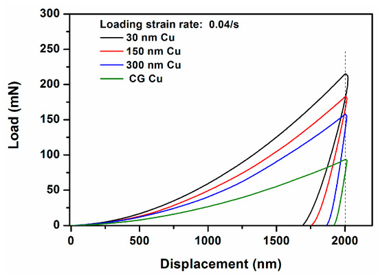
Figure 2.
Several load-displacement (P-h) curves obtained at an indentation depth of 2000 nm at of 0.04/s in the NC/UFG/CG Cu.

Table 1.
hf/hmax of NC/UFG/CG Cu obtained at a strain rate of 0.04/s and indentation depth of 2000 nm.
LCM images can be used to determine the extent and nature of the pile-up in the deformed surface morphology of the impression. Figure 3 gives of the residual morphology of the Berkovich indenter after loading at a strain rate of 0.04/s and the same indentation depth of 2000 nm in these four NC/UFG/CG Cu samples. Clearly, except the indents of 30 nm Cu exhibiting very little protrusion, the other three materials exhibit an obvious pile-up effect in the vicinities of the impression. In order to quantify the pile-up height along the z-axis in the impression, 20 cross-sectional lines perpendicular to each side of the indentation edges were measured (the left graphs in the Figure 3). The right image in Figure 3 gives the corresponding three-dimensional graphs of these four materials at x, y, and z axis angles of 59°, 274°, and 4°, which could better display the pile-up morphology of the indenter edge. Figure 4 gives the detailed maximum height of the pile-up (hpile-up) along the three different directions. It can be seen that the hpile-up would reach the maximum value as the grain size increases from 30 nm to 300 nm, followed by a slight decrease in the CG Cu. Besides that, there is another interesting result that the hpile-up in the CG Cu obviously deviates from the center of each of the indenter sides.
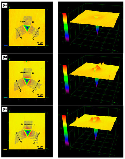
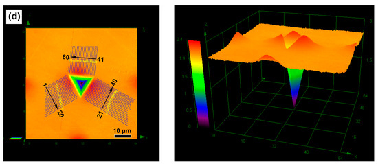
Figure 3.
LCM images of 30 nm Cu (a); 150 nm Cu (b); 300 nm Cu (c); and CG Cu (d) obtained at a strain rate of 0.04/s and the indentation depth of 2000 nm. The left side gives the places where hpile-up is measured and the right gives the corresponding three-dimensional graphs.
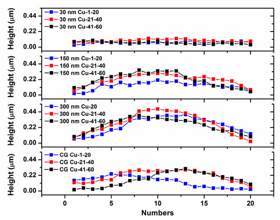
Figure 4.
The values of the hpile-up around the three indenter edges in the 30 nm Cu, 150 nm Cu, 300 nm Cu, and CG Cu.
3.3. Correction to the Hardness and Modulus from Pile-up Measurements
Taking the pile-ups of the residual impression into account, the projected area should be calibrated in order to yield relatively accurate values of E and H. A method exploiting the topography measurements to correct the values of these two mechanical parameters was proposed by Renner as the following procedures [11]:
where is the project contact area between the indenter and the material defined by the Oliver-Pharr method [1].
where is the constant dependent on the sharp of the indenter, and is the contact depth at .
where is the geometrical constant of 0.75 depending on the indenter shape and is the stiffness measured at .
is the reduced elastic modulus, having a equation of . and are the Young’s modulus and the Poisson’s ratio of the indenter, respectively.
It can be seen that the Oliver-Pharr method only considers that the sink-in event would occur at maximum displacement in the tested materials, while the pile-up issues are usually neglected. As shown in Figure 5, a better approximation of the real projected contact area can be defined by the following equations:
where N is the number of pile-ups formed around the indentation imprint and is the projection angle of the pile-up contact area on the indented plane. and are the maximum height and width of the ith pile-up, respectively. The contact surface between the pile-ups and the indenter can be treated as a triangle, and its dimensions are used to determine the values of and . Figure 5 gives an example of the 300 nm Cu sample mentioned in the text. The pile-up corrections of the E and H in the NC/UFG/CG Cu by Equations (5) and (6) are drawn in Figure 6. It can be seen that a larger would lower the values of the E and H.
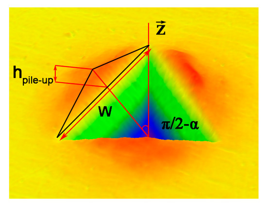
Figure 5.
Approximation of the real projected contact area resulting from pile-up formation: the maximum height and width of each pile-up around the imprint are considered to determine the projected area using triangles, and the imprints depict one typical example from the 300 nm Cu mentioned in the text.
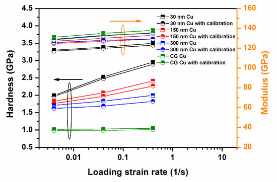
Figure 6.
E and H values without and with pile-up corrections as a function of the loading strain rate for 30 nm, 150 nm, 300 nm, and CG Cu.
3.4. Strain Rate Sensitivity and Activation Volume
To give a quantitative measurement of the strain rate dependence of hardness in the different materials, the strain rate sensitivity (m) and activation volume (v) obtained by the equations of and . Figure 7a,b give the m and v of the NC/UFG/CG Cu obtained at three typically different loading strain rates of 0.4/s, 0.04/s, and 0.004/s. The m decreases with the grain size while v presents an opposite tendency, and their values in these four materials are 0.08414, 0.05482, 0.02564, and 0.00549, and 6.06b3, 11.47b3, 27.99b3, and 194.17b3, respectively, where b = 0.256 nm is the Burgers vector for the ½{1 1 0} dislocation in the Cu.
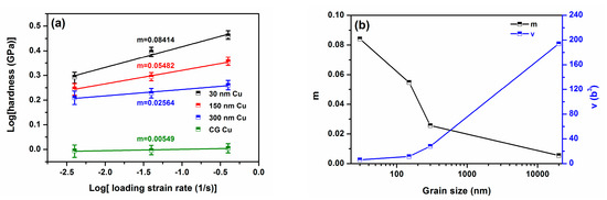
Figure 7.
The hardness versus loading strain rate () curves for measuring the m values of NC/UFG/CG Cu measured at three different of 0.4/s, 0.04/s, and 0.004/s at room temperature (a); The corresponding m and v versus grain size curves (b).
4. Discussion
Finite element modeling (FEM) results have pointed out that [17], as the hf/hmax is larger than 0.7, and/or in the materials without obvious work harden, a larger amount of the pile-up would directly induce an underestimation of the contact area, which further produces correspondingly large errors in the measurement (overestimation) of the E and H at smaller indentation depths. Our experimental results show that although all of the values of hf/hmax in these four materials are larger than 0.7, the height of the pile-up does not exhibit a continuously increasing tendency as the values become larger. The pile-up evolution during the indentation is closely related to the relative amounts of elastic and plastic deformation as characterized by the ratio of the elastic modulus to yield stress, i.e., . As , the contact is strictly elastic and dominated by sink-in in the way prescribed by Hertzian contact mechanics. As , the indentation process follows the rigid-plastic deformation and extensive pile-up would occur around the residual impression [7]. Our previous reports have already systematically studied the tensile properties of NC/UFG Cu with different grain sizes [14,16,18], and the corresponding values of in these four materials were found to be 175 (30 nm Cu), 264 (150 nm Cu), 386 (300 nm Cu), and 1930 (CG Cu). As expected, the elastic behavior is larger for the NC Cu because of smaller hf/hmax value, but there is little recovery for materials with larger grain size due to the fact that sufficiently larger plasticity occurs in these materials. These different elastic-plastic behaviors are closely related to the distinct deformation mechanism transformation as the grain size decreases below 500 nm.
Many studies have reported that introducing a larger volume of the GB structure could enhance m values in NC metals, such as NC Ni [16,19], NC Cu [14,15,16], nanotwinned Cu [20], NC Ta [21], and NC Mg [22]. The rate sensitivity of the mechanical properties is related to the thermally activated process of overcoming the obstacles of the glissile dislocation movement, which are normally expressed by the activation volume (v) of the thermally activated event. If the estimated v is less than 2b3 or even on the order of one atomic volume (b3), this may suggest that the deformation mechanism totally stems from the GB activities, such as the GB sliding/diffusion or even Coble creep, which can control the plasticity of NC metals. For the v in our 30 nm Cu, it is certainly much larger than the 2b3. This arises from the interactions between dislocations and GBs, including full/partial dislocation emission and absorption, de-pinning of dislocations impeded by GB ledges of impurities, and dynamic recovery of dislocations that reside along GBs. It should be noted that the activation volume of the face center cubic (FCC) metals can be also expressed as the equation of [23], where is the distance swept out by the glide dislocation during one activation event that can be treated as an approximate constant of b, and l is the length of dislocation segment involved in the thermal activation. As the grain size continuously increases, the forest dislocation density inside the grains is expected to increase, whereas the obstacle density associated with GBs decreases. This means that both the proportion of plastic deformation controlled by the dislocation motion and l become larger, which directly enhances the values of v. When the grain size increases to several micrometers, i.e., CG metals, conventional forest dislocation movement generated in the intragranular sources would dominate the plastic deformation and l is much larger, leading to the largest v obtained in our CG Cu. This deformation mechanism transformation varying with the grain size can well explain why the pile-up effect would gradually weaken or even disappear as the grain size decreases to a nano-regime.
For the NC Cu, more GBs are involved in the indentation deformation and both dislocation activity and GB sliding can be activated in the strain rate range studied. In this case, a large amount of slip planes are activated and dislocations emitted from GBs would propagate in the grain interior and be absorbed by the opposite GBs. This indicates that the highly mobile or unstable generated dislocations in the loading regime can only stay temporarily in the grain interior, because GB serves as a sink for dislocation absorption, and the materials exhibit very limited strain hardening capabilities (as shown in Figure 8a). Therefore, the effect of the pile-up induced by the strain hardening becomes invalid. Besides that, because of the limited intragranular space and GB activities such as GB sliding and rotation in NC metals, dislocation gliding occurs only on fewer slip systems and high stress concentration created in some local regions such as triple junctions would relax, which could reduce the number of the dislocations and further weaken pile-up lateral extension around the imprints.
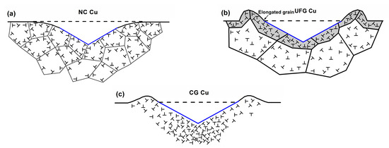
Figure 8.
Schematic illustrations of local GB structures and dislocation distribution in the NC (a); UFG (b); and CG (c) Cu underneath the indenters, where “T” represents dislocation.
As the grain size enters the ranges of 100–1500 nm, although a number of GB mechanisms such as GB sliding and GB rotation would participate in their plastic deformation, the transition between intragranular and intergranular deformation mechanism is not supposed to be abrupt [14,16,19,21,22,24]. Dislocation activities such as the cross- and multiple-slips from the internal source can still be activated effectively in the large grain zones, and dislocations can be trapped inside the grains as a result of dislocation interactions between slip systems or with debris left by cross-slip. So, some parts of the pile-up can form in a way similar to that in the CG metals, where strain hardening induces plastic deformation around the surface (see below). However, previous studies have demonstrated that many grains in the UFG Cu would have severely elongated grains under larger plastic deformation in the tensile tests [25,26]. For the nanoindentation tests, the top surface around the indenter has the largest deformation during the total deformation process, and thus it can be deduced that the grains in these regions possibly have elongated grains (as shown in Figure 8b). This means that the pile-up lateral extension and propagation of dislocation slip are possibly confined in the regions around the plastic zone, and the severely deformed grains would produce additional plasticity around the indenter, leading to the highest hpile-up in the UFG Cu with a grain size of 300 nm.
For conventional CG metals, plastic deformation mainly involves the dislocation multiplication from the intragranular Frank-Read sources, which could produce the dislocation cells/walls/networks structure in the grain interior. These formed microstructures, representing a strong pinning point to the dislocation-bowing segment, would suppress dislocation cross slips, leading to strong strain hardening in the subsequent plasticity. FEM results have revealed that due to the higher stress applied underneath the tip of the indenter, the shear strain or dislocation density generated at the deepest areas is much higher compared with other areas, and materials around this region harden more severely [8]. The strain hardening generated by such dislocation activities is more effective in suppressing the strain localization. However, for the regions approaching the surface, the dislocation slips in the other <110> directions would become relatively easy, which contributes to the final topography of the pile-up. Unlike the above NC/UFG metals, the CG Cu has a larger grain size and thus is assumed that the local material behavior is within the single crystalline which cannot be influenced by the neighboring grains. So, the plastic zone around the imprints in the CG Cu cannot be confined by the GB structure in the UFG Cu and the pile-up lateral extension thus declines to som extent (as shown in Figure 8c). Additionally, Renner claimed that the pile-up sizes and distributions such as height and lateral extension depend on the crystallographic directions and indenter disorientation, which are also the main reasons for generating significant asymmetries around imprints in CG metals [11].
5. Conclusions
Nanoindentation tests were carried out on crystalline Cu with different grain sizes ranging from 30 nm to 300 nm as well as CG Cu, and the residual indenter morphologies of these four materials were systematically studied. It can be observed that the height of the pile-up reaches the maximum value as the grain size increases from 30 nm to 300 nm, and then decreases in the CG Cu. Our analysis argued that dislocation activity and GB activities in the NC metals, some cross- and multiple-slips dislocation insides the larger grain in the UFG Cu, and forest dislocations from the intragranular Frank-Read sources in the CG Cu are responsible for the distinct pile-up effect in these materials.
Acknowledgments
This work was supported by the National Natural Science Foundation of China (Grant Nos. 11727803, 11672356 and 51371089) and Innovation team in key areas of Shaanxi Province (2016KCT-30).
Author Contributions
Jiangjiang Hu conducted the experiments and wrote the paper. Yusheng Zhang supervised the revised the whole work. Weiming Sun processed the data. Taihua Zhang conceived the work and revised the paper.
Conflicts of Interest
The authors declare no conflict of interest.
References
- Oliver, W.C.; Pharra, G.M. Measurement of hardness and elastic modulus by instrumented indentation: Advances in understanding and refinements to methodology. J. Mater. Res. 2004, 19, 3–20. [Google Scholar] [CrossRef]
- McElhaney, K.W.; Vlassak, J.J.; Nix, W.D. Determination of indenter tip geometry and indentation contact area for depth-sensing indentation experiments. J. Mater. Res. 1998, 13, 1300–1306. [Google Scholar] [CrossRef]
- Gale, J.D.; Achuthan, A. The effect of work-hardening and pile-up on nanoindentation measurements. J. Mater. Sci. 2014, 49, 5066–5075. [Google Scholar] [CrossRef]
- Beegan, D.; Chowdhury, S.; Laugier, M.T. A nanoindentation study of copper films on oxidised silicon substrates. Surf. Coat. Technol. 2003, 176, 124–130. [Google Scholar] [CrossRef]
- Rodríguez, J.; Maneiro, M.A.G. A procedure to prevent pile up effects on the analysis of spherical indentation data in elastic-plastic materials. Mech. Mater. 2007, 39, 987–997. [Google Scholar] [CrossRef]
- Zhou, L.; Yao, Y. Single crystal bulk material micro/nano indentation hardness testing by nanoindentation instrument and AFM. Mater. Sci. Eng. 2007, 460–461, 95–100. [Google Scholar] [CrossRef]
- Taljat, B.; Pharr, G.M. Development of pile-up during spherical indentation of elastic-plastic solids. Int. J. Solids Struct. 2004, 41, 3891–3904. [Google Scholar] [CrossRef]
- Liu, Y.; Varghese, S.; Ma, J.; Yoshino, M.; Lu, H.; Komanduri, R. Orientation effects in nanoindentation of single crystal copper. Int. J. Plast. 2008, 24, 1990–2015. [Google Scholar] [CrossRef]
- Demiral, M.; Roy, A.; El Sayed, T.; Silberschmidt, V.V. Influence of strain gradients on lattice rotation in nano-indentation experiments: A numerical study. Mater. Sci. Eng. 2014, 608, 73–81. [Google Scholar] [CrossRef]
- Sánchez-Martín, R.; Pérez-Prado, M.T.; Segurado, J.; Molina-Aldareguia, J.M. Effect of indentation size on the nucleation and propagation of tensile twinning in pure magnesium. Acta Mater. 2015, 93, 114–128. [Google Scholar] [CrossRef]
- Renner, E.; Gaillard, Y.; Richard, F.; Amiot, F.; Delobelle, P. Sensitivity of the residual topography to single crystal plasticity parameters in Berkovich nanoindentation on FCC nickel. Int. J. Plast. 2016, 77, 118–140. [Google Scholar] [CrossRef]
- Petryk, H.; Stupkiewicz, S.; Kucharski, S. On direct estimation of hardening exponent in crystal plasticity from the spherical indentation test. Int. J. Solids Struct. 2017, 112, 209–221. [Google Scholar] [CrossRef]
- Chen, T.; Tan, L.; Lu, Z.; Xu, H. The effect of grain orientation on nanoindentation behavior of model austenitic alloy Fe-20Cr-25Ni. Acta Mater. 2017, 138, 83–91. [Google Scholar] [CrossRef]
- Hu, J.; Han, S.; Sun, G.; Sun, S.; Jiang, Z.; Wang, G.; Lian, J. Effect of strain rate on tensile properties of electric brush-plated nanocrystalline copper. Mater. Sci. Eng. 2014, 618, 621–628. [Google Scholar] [CrossRef]
- Hu, J.; Sun, G.; Zhang, X.; Wang, G.; Jiang, Z.; Han, S.; Zhang, J.; Lian, J. Effects of loading strain rate and stacking fault energy on nanoindentation creep behaviors of nanocrystalline Cu, Ni-20 wt.% Fe and Ni. J. Alloys Compd. 2015, 647, 670–680. [Google Scholar] [CrossRef]
- Hu, J.; Zhang, J.; Jiang, Z.; Ding, X.; Zhang, Y.; Han, S.; Sun, J.; Lian, J. Plastic deformation behavior during unloading in compressive cyclic test of nanocrystalline copper. Mater. Sci. Eng. 2016, 651, 999–1009. [Google Scholar] [CrossRef]
- Bolshakova, A.; Pharr, G.M. Influences of pileup on the measurement of mechanical properties by load and depth sensing indentation techniques. J. Mater. Res. 1998, 13, 1049–1058. [Google Scholar] [CrossRef]
- Zhang, H.; Jiang, Z.; Lian, S.; Jiang, Q. Strain rate dependence of tensile ductility in an electrodeposited Cu with ultrafine grain size. Mater. Sci. Eng. 2008, 479, 136–141. [Google Scholar] [CrossRef]
- Li, H.; Liang, Y.; Zhao, L.; Hu, J.; Han, S.; Lian, J. Mapping the strain-rate and grain-size dependence of deformation behaviors in nanocrystalline face-centered-cubic Ni and Ni-based alloys. J. Alloys Compd. 2017, 709, 566–574. [Google Scholar] [CrossRef]
- Wei, Y. The kinetics and energetics of dislocation mediated de-twinning in nano-twinned face-centered cubic metals. Mater. Sci. Eng. 2011, 528, 1558–1566. [Google Scholar] [CrossRef]
- Hu, J.; Sun, W.; Jiang, Z.; Zhang, W.; Lu, J.; Huo, W.; Zhang, Y.; Zhang, P. Indentation size effect on hardness in the body-centered cubic coarse-grained and nanocrystalline tantalum. Mater. Sci. Eng. 2017, 686, 19–25. [Google Scholar] [CrossRef]
- Hu, J.; Zhang, W.; Bi, G.; Lu, J.; Huo, W.; Zhang, Y. Nanoindentation creep behavior of coarse-grained and ultrafine-grained pure magnesium and AZ31 alloy. Mater. Sci. Eng. 2017, 698, 348–355. [Google Scholar] [CrossRef]
- Wei, Q.; Cheng, S.; Ramesh, K.T.; Ma, E. Effect of nanocrystalline and ultrafine grain sizes on the strain rate sensitivity and activation volume: Fcc versus bcc metals. Mater. Sci. Eng. 2004, 381, 71–79. [Google Scholar] [CrossRef]
- Jiang, Z.; Liu, X.; Li, G.; Jiang, Q.; Lian, J. Strain rate sensitivity of a nanocrystalline Cu synthesized by electric brush plating. Appl. Phys. Lett. 2006, 88, 143115. [Google Scholar] [CrossRef]
- Wei, Q.; Jia, D.; Ramesh, K.T.; Ma, E. Evolution and microstructure of shear bands in nanostructured Fe. Appl. Phys. Lett. 2002, 81, 1240. [Google Scholar] [CrossRef]
- Wei, Q.; Kecskes, L.; Jiao, T.; Hartwig, K.T.; Ramesh, K.T.; Ma, E. Adiabatic shear banding in ultrafine-grained Fe processed by severe plastic deformation. Acta Mater. 2004, 52, 1859–1869. [Google Scholar] [CrossRef]
© 2017 by the authors. Licensee MDPI, Basel, Switzerland. This article is an open access article distributed under the terms and conditions of the Creative Commons Attribution (CC BY) license (http://creativecommons.org/licenses/by/4.0/).